

Page 1
General Description
The MAX6610/MAX6611 are precise, low-power analog
temperature sensors combined with a precision voltage
reference. They are ideal for applications involving analog-to-digital converters (ADCs), where the MAX6610/
MAX6611 provide the reference voltage for the ADC
and develop a temperature output voltage that is
scaled to provide convenient ADC output codes. An 8bit ADC’s LSB is equal to 1°C, while a 10-bit ADC’s LSB
corresponds to 0.25°C.
The MAX6610/MAX6611 are available in two versions.
The MAX6611 operates from a 4.5V to 5.5V power supply and has a 4.096V reference output. The MAX6610
operates from 3.0V to 5.5V and has a 2.560V reference
output. Power-supply current is less than 150µA (typ).
Both the MAX6610/MAX6611 are available in a 6-pin
SOT23 package and operate from -40°C to +125°C.
Applications
System Temperature Monitoring
Temperature Compensation
HVAC
Home Appliances
Features
♦ ±1°C Accuracy
♦ Low TC Reference (±10ppm, typ)
♦ Temperature Output Scaled for ADCs
♦ Integrated Reference Voltage Scaled for
Convenient ADC Bit Weights
♦ No Calibration Required
♦ Low Supply Current
♦ Tiny 6-Pin SOT23 Package
♦ Low-Current Shutdown Mode
MAX6610/MAX6611
Precision, Low-Power, 6-Pin SOT23
Temperature Sensors and Voltage References
________________________________________________________________ Maxim Integrated Products 1
Ordering Information
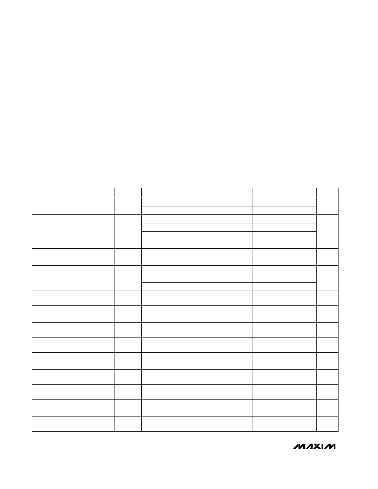
µC
REF IN
ADC IN
REF
TEMP
GND
GND
V
CC
V
CC
V
CC
GND
0.1µF
1nF
MAX6610
MAX6611
1nF
SHDN
Typical Application Circuit
19-2457; Rev 2; 11/03
For pricing, delivery, and ordering information, please contact Maxim/Dallas Direct! at
1-888-629-4642, or visit Maxim’s website at www.maxim-ic.com.
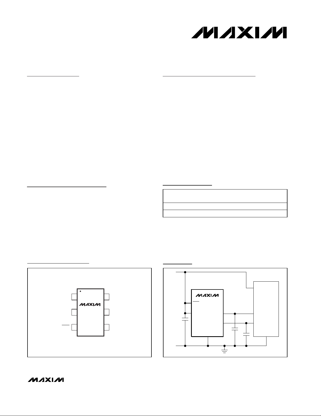
Pin Configuration
GND
TEMP
16GND
5 REF
V
CC
MAX6610
MAX6611
SOT23
TOP VIEW
2
34SHDN
PART
MAX6610AUT-T -40°C to +125°C 6 SOT23-6 2.560 ABDO
MAX6611AUT-T -40°C to +125°C 6 SOT23-6 4.096 ABOP
TEMP
RANGE
PINPACKAGE
V
REF
(V)
TOP
MARK
Page 2
MAX6610/MAX6611
Precision, Low-Power, 6-Pin SOT23
Temperature Sensors and Voltage References
2 _______________________________________________________________________________________
ABSOLUTE MAXIMUM RATINGS
ELECTRICAL CHARACTERISTICS
(VCC= 3.0 to 5.5V (MAX6610), VCC= 4.5V to 5.5V (MAX6611), TA= T
MIN
to T
MAX
, unless otherwise noted. Typical values are at V
CC
= 5.0V (MAX6611) and VCC= 3.3V (MAX6610), TA= +25°C.) (Note 1)
Stresses beyond those listed under “Absolute Maximum Ratings” may cause permanent damage to the device. These are stress ratings only, and functional
operation of the device at these or any other conditions beyond those indicated in the operational sections of the specifications is not implied. Exposure to
absolute maximum rating conditions for extended periods may affect device reliability.
Voltages Referenced to GND
VCC........................................................................-0.3V to +6.0V
All Other Pins............................................. -0.3V to (VCC+ 0.3V)
Input Current ...................................................................... 20mA
Output Current ....................................................................20mA
Continuous Power Dissipation (T
A
= +70°C)
6-Pin SOT23 (derate 8.7mW/°C above +70°C) ........695.7mW
Operating Temperature Range (T
MIN
, T
MAX
)....-40°C to +125°C
ESD Protection (all pins, Human Body Model) ..................2000V
Storage Temperature Range ............................-65°C to +150°C
Junction Temperature......................................................+150°C
Lead Temperature (soldering, 10s) ................................+300°C
Supply Current I
Temperature Sensor Error
Temperature Sensor Output
Voltage
Temperature Sensor Nonlinearity TA = -10°C to +80°C1°C
Temperature Sensor Output Slope
Temperature Sensor Supply
Sensitivity
Temperature Sensor Load
Regulation
Temperature Sensor Capacitive
Load
Temperature Sensor Long-Term
Stability
Reference Output Voltage V
Voltage Reference Temperature
Coefficient
Voltage Reference Line
Regulation
Voltage Reference Load
Regulation
Voltage Reference Long-Term
Stability
PARAMETER SYMBOL CONDITIONS MIN TYP MAX UNITS
Outputs unloaded 150 250
CC
SHDN = 0 0.2 1
TA = +25°C -1.2 +1.2
TA = -10°C to +55°C (Note 2) -2.4 +2.4
TA = -20°C to +85°C (Note 2) -3.7 +3.7
= -40°C to +125°C (Note 2) -5.0 +5.0
T
A
V
∆V
∆I
∆V
TEMP
time
MAX6611, TA = 0°C 1.200
MAX6610, TA = 0°C 0.750
MAX6611 16
MAX6610 10
3.0V ≤ VCC ≤ 5.5V for MAX6610 and 4.5V ≤
V
≤ 5.5V for MAX6611
CC
Sourcing: 0 ≤ I
Sinking: -100µA ≤ I
No sustained oscillations (Note 3) 0 0.2 µF
= +50°C for 1000hr ±0.1 °C
T
A
MAX6611, TA = +25°C 4.076 4.096 4.116
REF
MAX6610, TA = +25°C 2.547 2.560 2.573
T
= -40°C to +85°C -50 ±10 +50 ppm/°C
A
Sourcing: 0 ≤ I
/
OUT
OUT
Sinking: -200µA ≤ I
/
OUT
1000h at T
= +25°C 50 ppm
A
≤ 500µA -1 -2.5 +1
OUT
≤ 0 -2.5 +5
OUT
≤ 1mA 1 2
OUT
≤ 0 4 20
OUT
-1 +1 mV/V
0.5 °C/V
µA
°C
V
mV/°C
°C/mA
V
Ω
Page 3

MAX6610/MAX6611
Precision, Low-Power, 6-Pin SOT23
Temperature Sensors and Voltage References
_______________________________________________________________________________________ 3
ELECTRICAL CHARACTERISTICS (continued)
(VCC= 3.0 to 5.5V (MAX6610), VCC= 4.5V to 5.5V (MAX6611), TA= T
MIN
to T
MAX
, unless otherwise noted. Typical values are at V
CC
= 5.0V (MAX6611) and VCC= 3.3V (MAX6610), TA= +25°C.) (Note 1)
Note 1: All parameters tested at room temperature. Values through temperature are guaranteed by design.
Note 2: Guaranteed to 4 sigma.
Note 3: Guaranteed by design.
Typical Operating Characteristics
(VCC= 5V, I
OUT
= 0V, TA= +25°C, unless otherwise specified.)
MAX6610
TEMPERATURE VOLTAGE
vs. TEMPERATURE
MAX6610 toc01
TEMPERATURE (°C)
TEMPERATURE VOLTAGE (V)
1109565 80-10 5 20 35 50-25
0.2
0.4
0.6
0.8
1.0
1.2
1.4
1.6
1.8
2.0
0
-40 125
SUPPLY CURRENT vs. SUPPLY VOLTAGE
MAX6610 toc03
SUPPLY VOLTAGE (V)
SUPPLY CURRENT (
m
A)
5.55.04.0 4.52.0 2.5 3.0 3.51.5
20
40
60
80
100
120
140
160
180
200
0
1.0 6.0
TA = +100°C
TA = +25°C
TA = -40°C
REFERENCE VOLTAGE ERROR
vs. TEMPERATURE
MAX6610 toc02
TEMPERATURE (°C)
REFERENCE VOLTAGE ERROR (%)
1109580655035205-10-25
0.04
0.05
0.06
0.07
0.08
0.09
0.10
0.03
-40 125
Voltage Reference Output Noise
Turn-On Settling Time
(V
Turn-On Settling Time
(V
Turn-On Settling Time
(SHDN to REF)
Turn-On Settling Time
(SHDN to TEMP)
PARAMETER SYMBOL CONDITIONS MIN TYP MAX UNITS
f = 0.1Hz to 10Hz 100 µV
f = 10Hz to 10kHz 100 µV
V
= 0 to 5V step, C
to REF)
CC
to TEMP)
CC
CC
= 0.1% of final value
V
REF
V
= 0 to 5V step, C
CC
= 1°C of final value
V
TEMP
SHDN = 0 to 5V step, C
V
= 0.1% of final value
REF
SHDN = 0 to 5V step, C
= 1°C of final value
V
TEMP
LOGIC INPUT (SHDN)
Logic Input High Voltage V
Logic Input Low Voltage V
Logic Input Leakage I
IH
IL
LEAK
SHDN = 5V, VCC = 5V 10 25
SHDN = 0V, VCC = 5V 0.1 1
LOAD
LOAD
LOAD
LOAD
= 50pF,
= 50pF,
= 50pF,
= 50pF,
VCC -
0.5
P-P
P-P
300 µs
500 µs
300 µs
500 µs
V
0.5 V
µA
Page 4

MAX6610/MAX6611
Detailed Description
The MAX6610/MAX6611 combine a temperature sensor
with a low-power voltage reference. The reference voltage and temperature sensor gain give convenient LSB
weights when used with an ADC.
For example, when an 8-bit ADC is used with the
MAX6610/MAX6611, an LSB is equivalent to 1°C and a
10-bit ADC LSB is equivalent to 0.25°C.
The reference output features a proprietary temperature-coefficient, curvature-correction circuit and lasertrimmed thin-film resistors that result in a low
temperature coefficient (50ppm/°C max) and initial
accuracy of ±0.5% max. The maximum supply current
is 250µA during normal operation and 1µA max during
shutdown. The supply voltage range is 3.0V to 5.5V for
the MAX6610 and 4.5V to 5.5V for the MAX6611.
Voltage Reference
The MAX6610/MAX6611 REF output provides a voltage
reference for ADCs or other system subcircuits. REF is
capable of driving loads of up to 1mA. An output
capacitor can be as large as 1µF.
The voltage reference provides scaled ADC conversions with bit weights that are in convenient units.
For the MAX6610 (2.56V REF output), an 8-bit ADC
yields 10mV/bit or 2.5mV/bit for a 10-bit ADC. The
MAX6611 (4.096V REF output) yields 16mV/bit for an 8bit ADC or 4mV/bit for a 10-bit ADC.
Temperature Sensor
The MAX6610/MAX6611 TEMP output provides an analog output voltage that is a linear function of its die temperature as defined by:
V
TEMP
= 1.2V + (T°C ✕ 16mV/°C) for the MAX6611
and
V
TEMP
= 0.75V + (T°C ✕ 10mV/°C) for the MAX6610
The slope of the output voltage is V
REF
/256 per °C
(16mV/°C for the MAX6611 and 10mV/° C for the
MAX6610). There is a +75°C offset on the temperature
output (The MAX6611’s output is 1.2V and, the
MAX6610’s output is 0.75V) at 0°C. The temperature error
is less than 1.2°C at TA= +25°C, less than ±3.8°C from
TA= -20°C to +85°C, and only ±5°C for TA= -40°C to
+125°C.
Shutdown
The MAX6610/MAX6611 are equipped with a shutdown
feature that, when driven low, shuts down all internal circuitry and reduces supply current to 1µA (max). When in
shutdown, REF is pulled to GND through a 150kΩ resistor and TEMP goes to a high-impedance state. For normal operation, connect SHDN to VCC.
Applications Information
Output/Load Capacitance
The MAX6610/MAX6611 TEMP output can drive capacitive loads up to 0.2µF. The MAX6610/MAX6611 REF
output can drive capacitive loads up to 1µF. Devices in
this family do not require an output capacitance for
dynamic stability. However, in applications where the
load or the supply can experience step changes, an
output capacitor within the specified range reduces the
amount of overshoot (or undershoot) and assists the
circuit’s transient response. Many applications do not
need an external capacitor, and this family can offer a
significant advantage in these applications when board
space is critical.
Supply Current
The quiescent supply current of the MAX6610/
MAX6611 is typically 150µA and is virtually independent of the supply voltage. Unlike shunt-mode references, the load current of series-mode references is
drawn from the supply voltage only when required, so
supply current is not wasted and efficiency is maximized over the entire supply voltage range. This
improved efficiency can help reduce power dissipation
and extend battery life.
Precision, Low-Power, 6-Pin SOT23
Temperature Sensors and Voltage References
4 _______________________________________________________________________________________
Pin Description
PIN NAME FUNCTION
1V
2 GND Ground
3 SHDN
4 TEMP
5 REF Reference Voltage Output
6 GND Must be connected to pin 2.
CC
Supply Voltage Input. Bypass to GND
with a 0.1µF capacitor.
Logic Level Shutdown Input (Active
Low). Driving SHDN with a logic low
turns off internal circuitry to reduce
supply current to 1µA (max).
Temperature Output Pin. Voltage at
TEMP varies linearly with temperature.
Page 5

Sensing Circuit Board and
Ambient Temperatures
Temperature sensor ICs, like the MAX6610/MAX6611
that sense their own die temperatures, must be mounted on, or close to, the object whose temperature they
are intended to measure. Because there is a good thermal path between the package’s metal leads and the
IC die, the MAX6610/MAX6611 can accurately measure
the temperature of the circuit board to which it is soldered. If the sensor is intended to measure the temperature of a heat-generating component on the circuit
board, it should be mounted as close as possible to
that component and should share supply and ground
traces (if they are not noisy) with that component where
possible. This maximizes the heat transfer from the
component to the sensor. The thermal path between
the plastic package and the die is not as good as the
path through the leads, so the MAX6610/MAX6611, like
all temperature sensors in plastic packages, are less
sensitive to the temperature of the surrounding air than
to the temperature of the leads. They can be successfully used to sense ambient temperature if the circuit
board is designed to track the ambient temperature.
As with any IC, the wiring and circuits must be kept
insulated and dry to avoid leakage and corrosion,
especially if the part is operated at cold temperatures
where condensation can occur.
Self-Heating
The MAX6610/MAX6611 are low-power circuits and are
intended to drive light loads. As a result, the temperature rise due to power dissipation on the die is insignificant under normal conditions.
For example, assume that the MAX6611 is operating
from a 5V supply at +50°C (V
TEMP
= 2V) and that the
temperature output is driving a 100kΩ load (I
TEMP
=
20µA). Also assume that the voltage reference is driving a 500µA load and the worst-case quiescent supply
current is used. In the 6-pin SOT23 package, the die
temperature increases above the ambient by 0.2°C.
Next, assume TEMP and REF are driving their maximum loads (I
TEMP
= 500µA and I
REF
= 1mA) and V
CC
= 5V, and TA= +50°C (V
TEMP
= 2V). Here, the die tem-
perature increases above the ambient by 0.4°C.
A first order for self-heating effects can be estimated
from temperature and reference load currents and the
previous supply voltage.
Chip Information
TRANSISTOR COUNT: 1346
PROCESS: BiCMOS
MAX6610/MAX6611
Precision, Low-Power, 6-Pin SOT23
Temperature Sensors and Voltage References
_______________________________________________________________________________________ 5
Page 6

MAX6610/MAX6611
Precision, Low-Power, 6-Pin SOT23
Temperature Sensors and Voltage References
Maxim cannot assume responsibility for use of any circuitry other than circuitry entirely embodied in a Maxim product. No circuit patent licenses are
implied. Maxim reserves the right to change the circuitry and specifications without notice at any time.
6 _____________________Maxim Integrated Products, 120 San Gabriel Drive, Sunnyvale, CA 94086 408-737-7600
© 2003 Maxim Integrated Products Printed USA is a registered trademark of Maxim Integrated Products.
Package Information
(The package drawing(s) in this data sheet may not reflect the most current specifications. For the latest package outline information,
go to www.maxim-ic.com/packages.)
6LSOT.EPS
PACKAGE OUTLINE, SOT-23, 6L
21-0058
1
F
1
 Loading...