

For pricing, delivery, and ordering information, please contact Maxim Direct at 1-888-629-4642,
or visit Maxim’s website at www.maxim-ic.com.
General Description
The MAX6605 precision, low-power, analog output temperature sensor is available in a 5-pin SC70 package.
The device has a +2.7V to +5.5V supply voltage range
and 10µA supply current over the -55°C to +125°C temperature range. For the -40°C to +105°C temperature
range, the supply voltage can go as low as +2.4V.
Accuracy is ±0.75°C at TA= +25°C and ±3°C from 0°C
to +70°C.
The MAX6605 output voltage is dependent on its die
temperature and has a slope of 11.9mV/°C and an offset of 744mV at 0°C. The output typically shows only
+0.4°C of nonlinearity over the -20°C to +85°C temperature range.
________________________Applications
Cellular Phones
Battery Packs
GPS Equipment
Digital Cameras
Features
♦ Low Current Consumption (10µA max)
♦ Small SC70 Package
♦ Accurate (±0.75°C at T
A
= +25°C)
♦ Optimized to Drive Large Capacitive Loads
MAX6605
Low-Power Analog Temperature Sensor
in SC70 Package
________________________________________________________________
Maxim Integrated Products
1
Typical Application Circuit
19-1840; Rev 3; 12/09
Ordering Information
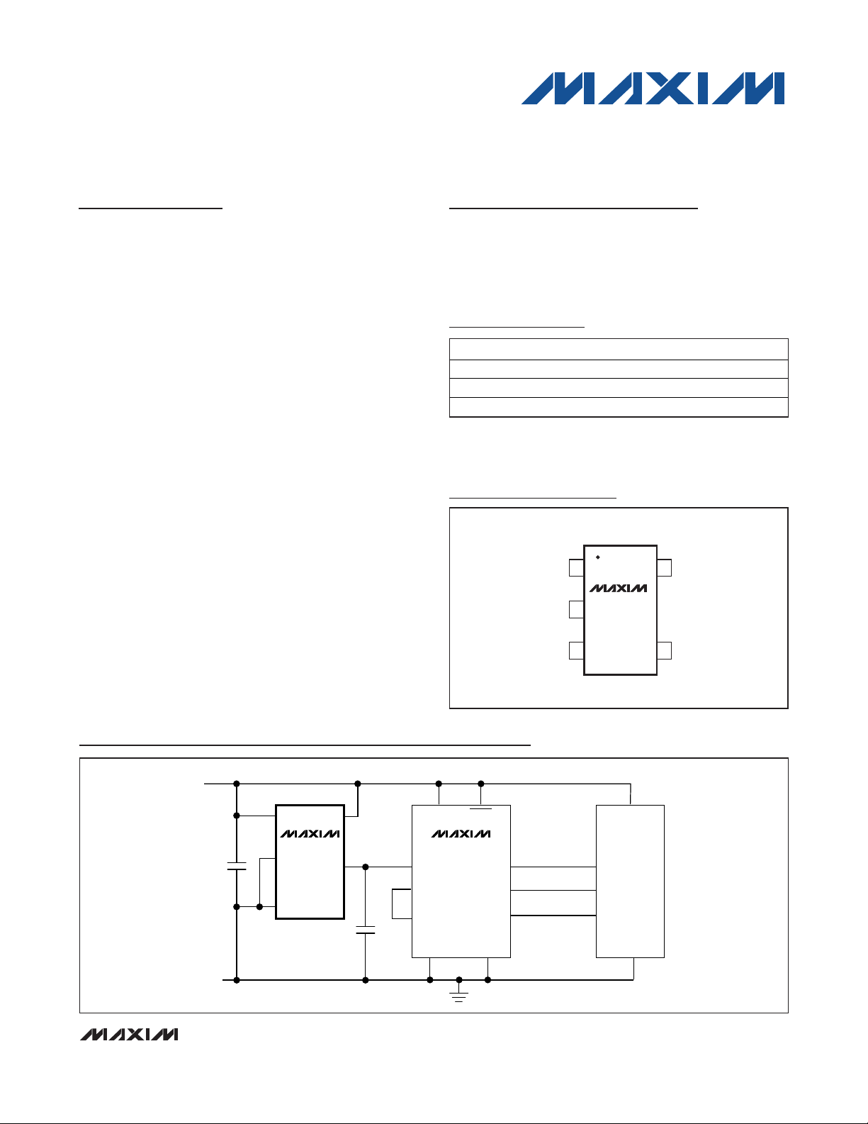
Pin Configuration
+
Denotes a lead(Pb)-free/RoHS-compliant package.
T = Tape and reel.
/V denotes an automotive qualified part.
PART TEMP RANGE PIN-PACKAGE
MAX6605MXK-T -55°C to +125°C 5 SC70-5
MAX6605MXK+T -55°C to +125°C 5 SC70-5
MAX6605MXK/V+T -40°C to +85°C 5 SC70-5
TOP VIEW
15GNDV
CC
MAX6605
2
A
34
V
CC
V
CC
CS = 0.1μF
GND
A
GND
B
MAX6605
IN+
REFOUT
REFIN
1nF
IN–
V
DD
MAX1106
SHDN
CONVSTOUT
SCLK
GND
BOUT
SC70
V
CC
CPU
I/O
I/O
I/ODOUT
GND
MAX6605
Low-Power Analog Temperature Sensor
in SC70 Package
2 _______________________________________________________________________________________
ABSOLUTE MAXIMUM RATINGS
ELECTRICAL CHARACTERISTICS
(V
CC
= +2.7V to +5.5V, CL= 1nF, TA= -55°C to +125°C, unless otherwise noted.) (Note 1)
Stresses beyond those listed under “Absolute Maximum Ratings” may cause permanent damage to the device. These are stress ratings only, and functional
operation of the device at these or any other conditions beyond those indicated in the operational sections of the specifications is not implied. Exposure to
absolute maximum rating conditions for extended periods may affect device reliability.
Note 1: All parameters are measured at TA= +25°C. Specifications over temperature range are guaranteed by design.
Note 2: Error (expressed in °C) is defined as the difference between the calculated and measured values of output voltage.
Guaranteed by design to 5 sigma.
V
CC
to GND..............................................................-0.3V to +6V
OUT, A, B to GND ......................................-0.3V to (V
CC
+ 0.3V)
ESD Protection (Human Body Model) ............................> 2000V
Current into Any Pin ............................................................10mA
Output Short-Circuit Duration.....................................Continuous
Continuous Power Dissipation (T
A
= +70°C)
5-Pin SC70 (derate 3.1mW/°C above +70°C)..............245mW
Operating Temperature Range .........................-55°C to +125°C
Junction Temperature......................................................+150°C
Storage Temperature Range .............................-65°C to +150°C
Lead Temperature (soldering, 10s) .................................+300°C
PARAMETER
CONDITIONS
UNITS
TA = +25°C
TA = -0°C to +70°C
Temperature Error
V
OUT
= 0.744 + (0.0119 × T°C) +
(1.604 × 10
-6
× T2)V (Note 2)
V
CC
= +3.3V
°C
TA = -55°C to +125°C
Supply Voltage V
CC
TA = -40°C to +105°C
V
Supply Current I
Q
No load
10 µA
Output Voltage V
OUT
TA = 0°C
mV
Nonlinearity TA = -20°C to +85°C
°C
Sensor Gain (Average Slope) TA = -40°C to +100°C
mV/°C
Capacitive Load Required for stability 1 nF
20
Load Regulation
T
A
= -55°C, I
OUT
= -10µA to +10µA 20
m°C/µA
SYMBOL
TA = -20°C to +85°C -3.8 +3.8
TA = -40°C to +100°C -5.0 +5.0
TA = -55°C to +125°C -5.8 +5.8
MIN TYP MAX
±0.75
-3.0 +3.0
2.7 5.5
2.4 5.5
4.5
744
0.4
11.1 11.9 12.7
TA = -20°C to +125°C, I
= -20µA to +20µA
OUT

MAX6605
Low-Power Analog Temperature Sensor
in SC70 Package
_______________________________________________________________________________________
3
Typical Operating Characteristics
(VCC= +3.3V, CS= 0.1µF, CL= 1nF, unless otherwise noted.)
OUTPUT VOLTAGE vs. TEMPERATURE
MAX6605 toc01
1.7
1.5
1.3
1.1
0.9
0.7
0.5
0.3
0.1
-0.1
-0.3
-0.5
TEMPERATURE ERROR (°C)
-0.7
-0.9
-1.1
-1.3
-55 -15-35 2556545 85 105 125
2.2
2.0
1.8
1.6
1.4
1.2
1.0
0.8
OUTPUT VOLTAGE (V)
0.6
0.4
0.2
0
-55 -15-35 2556545 10585 125
TEMPERATURE (°C)
SUPPLY CURRENT
vs. TEMPERATURE
7
6
VCC = +5V
5
4
3
SUPPLY CURRENT (μA)
2
1
0
-55 -15 5-35 25 45 65 85 105 125
VCC = +2.4V
TEMPERATURE (°C)
VCC = +3.3V
1.060
1.055
MAX6605 toc04
1.050
1.045
1.040
1.035
OUTPUT VOLTAGE (V)
1.030
1.025
1.020
021 3456
TEMPERATURE ERROR
vs. TEMPERATURE
TEMPERATURE (°C)
OUTPUT VOLTAGE
vs. SUPPLY VOLTAGE
TA = +25°C
SUPPLY VOLTAGE (V)
MAX6605 toc02
MAX6605 toc05
500mV/div
SUPPLY CURRENT
vs. SUPPLY VOLTAGE
6
5
4
3
2
SUPPLY CURRENT (μA)
1
0
023145
SUPPLY VOLTAGE (V)
TA = +25°C
MAX6605 toc03
STEP-RESPONSE FROM +25°C TO +100°C
(FLUORINERT BATH)
MAX6605 toc06
OUT
0
1s/div

Detailed Description
The MAX6605 analog output temperature sensor’s output voltage is a linear function of its die temperature.
The slope of the output voltage is 11.9mV/°C, and there
is a 744mV offset at 0°C to allow measurement of negative temperatures. The MAX6605 has three terminals:
VCC, GND, and OUT. The maximum supply current is
10µA, and the supply voltage range is from +2.4V to
+5.5V for the -40°C to +105°C temperature range and
+2.7V to +5.5V for the -55°C to +125°C temperature
range. The temperature error is <1°C at TA= +25°C,
<3.8°C from TA= -20°C to +85°C, and <5.8°C from T
A
= -55°C to +125°C.
Nonlinearity
The benefit of silicon analog temperature sensors over
thermistors is linearity over extended temperatures. The
nonlinearity of the MAX6605 is typically 0.4°C over the
-20°C to +85°C temperature range.
Transfer Function
The temperature-to-voltage transfer function has an
approximately linear positive slope and can be
described by the equation:
V
OUT
= 744mV + (T ✕11.9mV/°C)
where T is the MAX6605’s die temperature in °C.
Therefore:
T (°C) = (V
OUT
- 744mV) / 11.9mV/°C
To account for the small amount of curvature in the
transfer function, use the equation below to obtain a
more accurate temperature reading:
V
OUT
= 0.744V + 0.0119V/°C ✕T(°C) +
1.604 ✕10-6V/°C
2
✕
(T(°C))
2
Applications Information
Sensing Circuit Board and
Ambient Temperatures
Temperature sensor ICs like the MAX6605 that sense
their own die temperatures must be mounted on, or
close to, the object whose temperature they are intended to measure. Because there is a good thermal path
between the SC70 package’s metal leads and the IC
die, the MAX6605 can accurately measure the temperature of the circuit board to which it is soldered. If the
sensor is intended to measure the temperature of a heatgenerating component on the circuit board, it should be
mounted as close as possible to that component and
should share supply and ground traces (if they are not
noisy) with that component where possible. This will maximize the heat transfer from the component to the sensor.
The thermal path between the plastic package and the
die is not as good as the path through the leads, so the
MAX6605, like all temperature sensors in plastic packages, is less sensitive to the temperature of the surrounding air than it is to the temperature of its leads. It can be
successfully used to sense ambient temperature if the circuit board is designed to track the ambient temperature.
As with any IC, the wiring and circuits must be kept insulated and dry to avoid leakage and corrosion, especially if
the part will be operated at cold temperatures where condensation can occur.
The thermal resistance junction to ambient (θ
JA
) is the
parameter used to calculate the rise of a device junction
temperature (TJ) due to its power dissipation. For the
MAX6605, use the following equation to calculate the rise
in die temperature:
TJ= TA+ θJA((VCCx IQ) + (VCC- V
OUT
) I
OUT
)
The MAX6605 is a very-low-power temperature sensor
and is intended to drive very light loads. As a result, the
temperature rise due to power dissipation on the die is
insignificant under normal conditions. For example,
assume that the MAX6605 is operating from a +3V supply at +21.6°C (V
OUT
= 1V) and is driving a 100kΩ load
(I
OUT
= 10µA). In the 5-pin SC70 package, the die tem-
perature will increase above the ambient by:
TJ- TA= θJA((VCCx IQ) + (VCC- V
OUT
) I
OUT
) =
324°C/W x ((3V x 10µA) + (3V - 1V) x 10µA) = 0.0162°C
Therefore, the error caused by power dissipation will be
negligible.
MAX6605
Low-Power Analog Temperature Sensor
in SC70 Package
4 _______________________________________________________________________________________
Pin Description
PIN NAME FUNCTION
1V
2 A Must be connected to GND.
3 OUT
CC
4 B Must be connected to VCC.
5 GND Ground
Supply Input. Decouple with a 0.1µF
capacitor to GND.
Temperature Sensor Output,
C
≥ 1nF
L

MAX6605
Low-Power Analog Temperature Sensor
in SC70 Package
_______________________________________________________________________________________ 5
Capacitive Loads
The MAX6605 can drive unlimited load capacitance.
For stable operation load capacitance should be >1nF.
Chip Information
TRANSISTOR COUNT: 573
PACKAGE TYPE PACKAGE CODE DOCUMENT NO.
5 SC70 X5-1
21-0076
Package Information
For the latest package outline information and land patterns,
go to www.maxim-ic.com/packages
. Note that a “+”, “#”, or
“-” in the package code indicates RoHS status only. Package
drawings may show a different suffix character, but the drawing
pertains to the package regardless of RoHS status.

MAX6605
Low-Power Analog Temperature Sensor
in SC70 Package
Maxim cannot assume responsibility for use of any circuitry other than circuitry entirely embodied in a Maxim product. No circuit patent licenses are
implied. Maxim reserves the right to change the circuitry and specifications without notice at any time.
6
_____________________Maxim Integrated Products, 120 San Gabriel Drive, Sunnyvale, CA 94086 408-737-7600
© 2009 Maxim Integrated Products Maxim is a registered trademark of Maxim Integrated Products, Inc.
Revision History
REVISION
NUMBER
0 10/00 Initial release —
1 8/04 — —
REVISION
DATE
DESCRIPTION
PAGES
CHANGED
2 11/08 Corrected the parameter unit for V
3 12/09 Added lead-free and automoti ve-qualif ied parts to the Ordering Information table. 1
in the Transfer Function section. 4
OUT
 Loading...