Maxim MAX6604 Datasheet

General Description
The MAX6604 high-precision temperature sensor is
designed for thermal monitoring functions in DDR memory modules. The device is readable and programmable
through the 2-wire SMBus™/I2C-compatible interface.
Three address inputs set the bus address for the temperature sensor to provide up to eight devices on one bus.
The internal thermal sensor continuously monitors the
temperature and updates the temperature data eight
times per second. The master can read the temperature data at any time. Since the thermal sensor is located on the memory module, temperature data recorded
accurately represents the temperature of the components on the module. Consequently, the MAX6604 provides a much more accurate measurement of module
temperature than techniques involving temperature
sensors on the motherboard. In addition, the device
responds more quickly to temperature changes on the
module than a motherboard sensor.
The MAX6604 also features an interrupt-output indicator for temperature-threshold monitoring. The threshold
levels are programmable through the digital interface.
The MAX6604 operates from -20°C to +125°C, and is
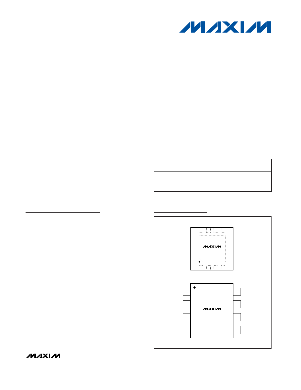
available in JEDEC-standard 8-pin TSSOP and TDFN
(MO-229-WCED-2) packages.
Applications
Memory Modules
Desktop Computers
Notebook Computers
Workstations
Networking Equipment
Features
♦ JEDEC Compliant
♦ ±1°C Temperature-Monitoring Accuracy
♦ Overtemperature Interrupt with Programmable
Threshold
♦ +2.7V to +3.6V Operating Voltage Range
♦ SMBus/I2C-Compatible Interface
♦ 300µA Typical Operating Current
♦ 3µA Typical Shutdown Current
♦ -20°C to +125°C Operating Temperature Range
♦ 8-Pin TSSOP and TDFN (MO-229-WCED-2)
Packages
MAX6604
Precision Temperature Monitor for
DDR Memory Modules
________________________________________________________________ Maxim Integrated Products 1
Ordering Information
19-3837; Rev 0; 10/05
For pricing, delivery, and ordering information, please contact Maxim/Dallas Direct! at
1-888-629-4642, or visit Maxim’s website at www.maxim-ic.com.
PART
PIN-PACKAGE
PKG
CODE
MAX6604ATA
8 TDFN-EP**
T823-1
MAX6604AHA
8 TSSOP H8-1
SMBus is a trademark of Intel Corporation.
Typical Application Circuit appears at end of data sheet.
134
865
V
CC
SCL SDA
MAX6604
MAX6604
2
7
EVENT
A0 A2 GNDA1
TDFN-EP**
TSSOP
TOP VIEW
SCL
SDA
GND
1
2
8
7
V
CC
EVENT
A1
A2A03
4
6
5
Pin Configurations
**EP = Exposed paddle.
TEMP RANGE
-20°C to +125°C
-20°C to +125°C
(MO229-WCED-2)

MAX6604
Precision Temperature Monitor for
DDR Memory Modules
2 _______________________________________________________________________________________
ABSOLUTE MAXIMUM RATINGS
ELECTRICAL CHARACTERISTICS
(VCC= +2.7V to +3.6V, TA= -20°C to +125°C, unless otherwise noted. Typical values are at VCC= +3.3V, TA= +25°C.) (Note 1)
Stresses beyond those listed under “Absolute Maximum Ratings” may cause permanent damage to the device. These are stress ratings only, and functional
operation of the device at these or any other conditions beyond those indicated in the operational sections of the specifications is not implied. Exposure to
absolute maximum rating conditions for extended periods may affect device reliability.
All Input and Output Voltages ..................................-0.3V to +6V
Continuous Power Dissipation (TA= +70°C)
8-Pin TDFN (derate 16.7mW/°C above +70°C) ......1333.3mW
8-Pin TSSOP (derate 8.1mW/°C above +70°C) ........646.7mW
ESD Protection (all pins, Human Body Model) ....................±2kV
Junction Temperature......................................................+150°C
Operating Temperature Range .........................-20°C to +125°C
Storage Temperature Range .............................-65°C to +150°C
Lead Temperature (soldering, 10s) .................................+300°C
PARAMETER
SYMBOL
CONDITIONS
MIN
TYP
MAX
UNITS
Operating Supply Voltage Range V
CC
V
°C
Temperature Resolution
11 bits
+3V ≤ VCC ≤ +3.6V, +75°C ≤ TA ≤ +95°C -1 +1
-2 +2
Temperature Accuracy
+3V ≤ V
CC
≤ +3.6V, -20°C ≤ TA ≤ +125°C -3 +3
°C
Power-On Reset (POR) Threshold VCC falling edge 2.0 V
POR Threshold Hysteresis 90 mV
Undervoltage-Lockout Threshold 2.4 V
Operating Current During conversion 0.3 0.5 mA
Standby Current 36µA
Conversion Time
125 ms
Conversion Rate
8Hz
DIGITAL INTERFACE (Note 2)
Log i c- Inp ut H i g h V ol tag e ( S C L, S D A)
V
IH
2.1 V
Logic-Input Low Voltage (SCL, SDA)
V
IL
0.8 V
Logic-Input Hysteresis (SCL, SDA) 500 mV
Leakag e C ur r ent ( E V E N T, S C L, S D A,
A2, A1, A0)
I
LEAK
V
IN
= GND or V
CC
-1 +1 µA
Logic-Output Low Voltage
(SDA, EVENT)
V
OL
I
PULL_UP
= 350µA 50 mV
Logic-Output Low Sink Current
(SDA, EVENT)
I
OL
VOL = 0.6V 6 mA
Input Capacitance (SCL, SDA) C
IN
5pF
Serial-Clock Frequency f
SCL
10 100 kHz
+2.7 +3.6
0.125
+3V ≤ V
t
CONV
f
CONV
≤ +3.6V, +40°C ≤ TA ≤ +125°C
CC

MAX6604
Precision Temperature Monitor for
DDR Memory Modules
_______________________________________________________________________________________ 3
ELECTRICAL CHARACTERISTICS (continued)
(VCC= +2.7V to +3.6V, TA= -20°C to +125°C, unless otherwise noted. Typical values are at VCC= +3.3V, TA= +25°C.) (Note 1)
PARAMETER
SYMBOL
CONDITIONS
MIN
TYP
MAX
UNITS
Bus Free Time Between STOP and
START Condition
t
BUF
4.7 µs
90% to 90% 4.7 µs
START Condition Hold Time
10% of SMBDATA to 90% of SMBCLK 4 µs
STOP Condition Setup Time
90% of SMBCLK to 10% of SMBDATA 4 µs
Clock Low Period t
LOW
10% to 10% 4.7 µs
Clock High Period t
HIGH
90% to 90% 4 µs
Data Hold Time
300 ns
Data Setup Time
90% of SMBDATA to 10% of SMBCLK 250 ns
Receive SCL/SDA Rise Time t
R
ns
Receive SCL/SDA Fall Time t
F
300 ns
Pulse Width of Spike Suppressed t
SP
050ns
Note 1: All parameters are tested at TA= +25°C. Specifications over temperature are guaranteed by design.
Note 2: Guaranteed by design.
Rep eat S TART C ond i ti on S etup Ti m et
SU:STA
t
HD:STA
t
SU:STO
t
HD:DAT
t
SU:DAT
1000

MAX6604
Precision Temperature Monitor for
DDR Memory Modules
4 _______________________________________________________________________________________
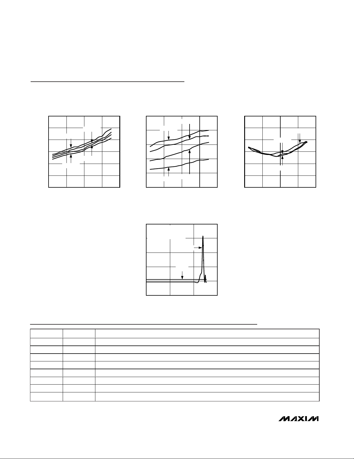
Typical Operating Characteristics
(Typical values are at VCC= +3.3V, TA= +25°C.)
0
2
1
4
3
5
6
-50 150
SHUTDOWN SUPPLY CURRENT
vs. TEMPERATURE
MAX6604 toc01
TEMPERATURE (°C)
SHUTDOWN SUPPLY CURRENT (µA)
0 50 100
VCC = 3.6V
VCC = 2.7V
VCC = 3.3V
VCC = 3.0V
340
360
320
300
280
260
-50 150
SUPPLY CURRENT
vs. TEMPERATURE
MAX6604 toc02
TEMPERATURE (°C)
SUPPLY CURRENT (µA)
0 50 100
VCC = 3.6V
VCC = 2.7V
VCC = 3.3V
VCC = 3.0V
-3
-1
-2
1
0
2
3
-50 150
TEMPERATURE ERROR
vs. TEMPERATURE
MAX6604 toc03
TEMPERATURE (°C)
TEMPERATURE ERROR (°C)
050100
VCC = 3.0V
VCC = 3.3V
VCC = 3.6V
2.5
2.0
1.5
1.0
0.5
0
0.1 100,000
TEMPERATURE ERROR
vs. POWER SUPPLY NOISE FREQUENCY
MAX6604 toc04
POWER SUPPLY NOISE FREQUENCY (kHz)
TEMPERATURE ERROR (°C)
10 1,000
SQUARE WAVE APPLIED
TO V
CC
WITH NO BYPASS
CAPACITOR
20mV
PP
200mV
PP
Pin Description
PIN NAME FUNCTION
1 A0 Address Input. Must connect to GND or VCC to set value.
2 A1 Address Input. Must connect to GND or VCC to set value.
3 A2 Address Input. Must connect to GND or VCC to set value.
4 GND Ground
5 SDA Serial-Data Input/Output. Open drain. Connect to a pullup resistor.
6 SCL Serial-Clock Input. Connect to a pullup resistor.
7 EVENT Event Output. Open drain. Connect to a pullup resistor.
8VCCSupply Voltage. Connect a 0.1µF capacitor to GND as close as possible to the device.

Detailed Description
The MAX6604 high-precision temperature sensor continuously monitors temperature and updates the
temperature data eight times per second. The device
functions as a slave on the SMBus/I2C-compatible interface. The master can read the temperature data at any
time through the digital interface. The MAX6604 also
features an open-drain, event-output indicator for temperature-threshold monitoring.
Serial Interface
SMBus/I2C
The MAX6604 is readable and programmable through
the SMBus/I
2
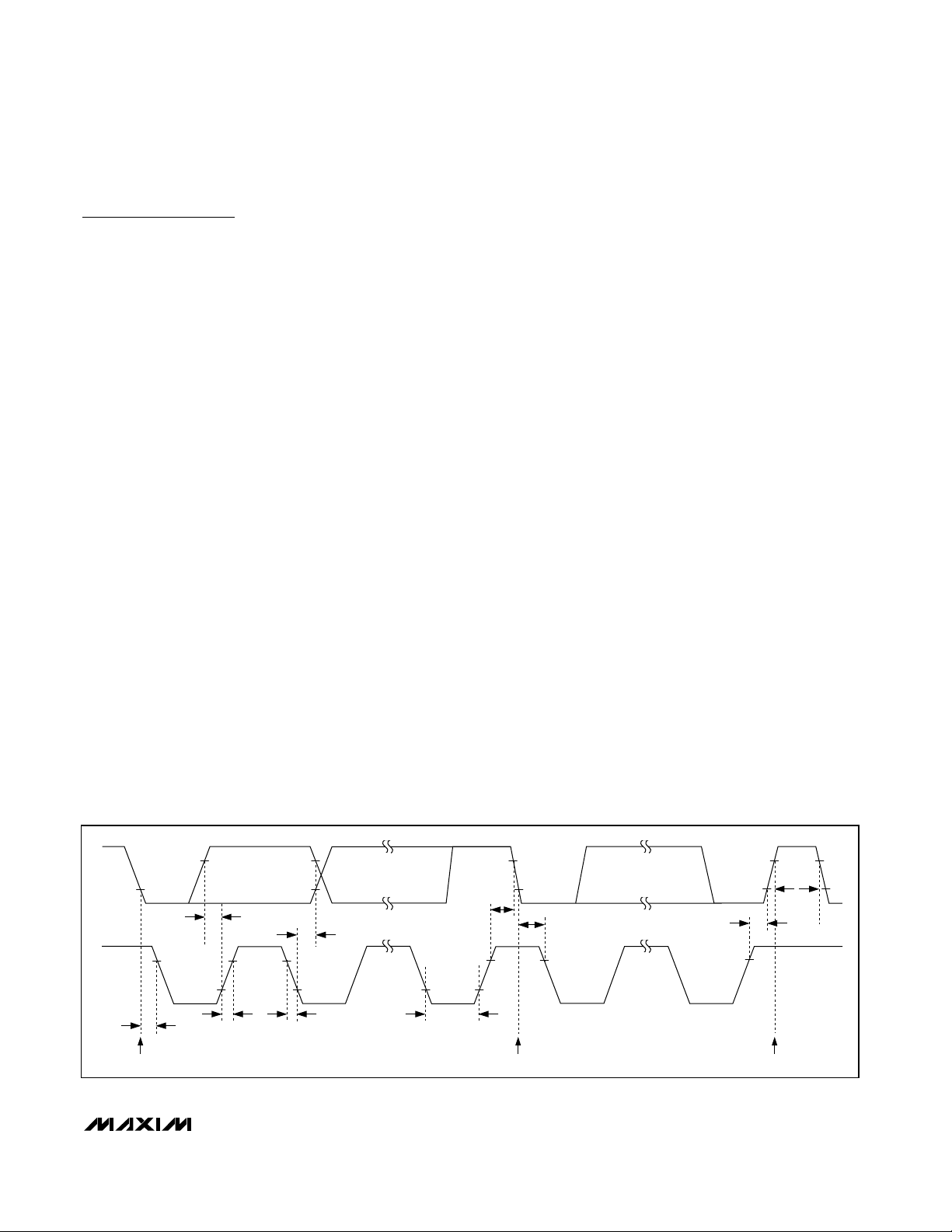
C-compatible interface. The device functions as a slave on the interface. Figure 1 shows the
general timing diagram of the clock (SCL) and the data
(SDA) signals for the SMBus/I2C-compatible interface.
The SDA and SCL bus lines are at logic-high when the
bus is not in use. Pullup resistors from the bus lines to
the supply are required when push-pull circuitry is not
driving the lines. The data on the SDA line can change
only when the SCL line is low. Start and stop conditions
occur when SDA changes state while the SCL line is
high (Figure 1). Data on SDA must be stable for the
duration of the setup time (t
SU:DAT
) before SCL goes
high. Data on SDA is sampled when SCL toggles high
with data on SDA is stable for the duration of the hold
time (t
HD:DAT
). Note that a segment of data is transmitted in an 8-bit byte. A total of nine clock cycles are
required to transfer a byte to the MAX6604. Since the
MAX6604 employs 16-bit registers, data is transmitted
or received in two 8-bit bytes (16 bits). The device
acknowledges the successful receipt for each byte by
pulling the SDA line low (issuing an ACK) during the
ninth clock cycle of each byte transfer.
From a software perspective, the MAX6604 appears as a
set of 16-bit registers that contain temperature data,
alarm threshold values, and control bits. A standard
SMBus/I2C-compatible, 2-wire serial interface reads temperature data and writes control bits and alarm threshold
data. Each device responds to its own SMBus/I2C slave
address, which is selected using A0, A1, and A2. See
the Device Addressing section for details.
The MAX6604 employs standard I2C/SMBus protocols
using 16-bit registers: write word and read word. Write
a word of data (16 bits) by first sending MAX6604’s I2C
address (0011-A2-A1-A0-0), then sending the 8-bit
command byte, followed by the first 8-bit data byte.
Note that the slave issues an acknowledge after each
byte is written. After the first 8-bit data byte is written,
the MAX6604 also returns an acknowledge. However,
the master does not generate a stop condition after the
first byte has been written. The master continues to
write the second byte of data with the slave acknowledging. After the second byte has been written, the
master then generates a stop condition. See Figure 2.
To read a word of data, the master generates a new
start condition and sends MAX6604’s I2C address with
the R/W bit high (1010-A2-A1-A0-1), then sends the 8bit command byte. Again, the MAX6604 issues an ACK
for each byte received. The master again sends the
device address, following an acknowledge. Next, the
master reads the contents of the selected register,
beginning with the most significant bit, and acknowledges if the most significant data byte is successfully
received. Finally, the master reads the least significant
data byte and issues a NACK, followed by a stop condition to terminate the read cycle.
MAX6604
Precision Temperature Monitor for
DDR Memory Modules
_______________________________________________________________________________________ 5
START CONDITION REPEATED START CONDITION STOP CONDITION
t
HD:STA
t
R
t
F
t
LOW
t
SU:DAT
t
HD:DAT
t
SU:STA
t
HD:STA
t
SU:STO
t
BUF
SDA
SCL
Figure 1. SDA and SCL Timing Diagram
 Loading...