

Page 1
General Description
The MAX6603 dual-channel, platinum RTD-to-voltage
signal conditioner excites and amplifies the signal from
two external 200Ω platinum-resistive temperature
devices (Pt RTD) to achieve high-voltage, level-filtered
signals for temperature measurements. The MAX6603
provides a direct ratiometric output voltage to simplify
the interface to microcontrollers with integrated analogto-digital converters (ADCs). External precision resistors and calibration processes are not needed. The
MAX6603 provides the necessary signal-conditioning
functions, including ratiometric excitation current,
amplification, buffered voltage outputs, diagnostic fault
detections, and input protection. The MAX6603 amplifies signals from two RTDs operating over the -40°C to
+1000°C temperature range and provides the temperature information as two independent analog voltages.
The MAX6603 features a ±6°C (max) accuracy over the
+400°C to +600°C temperature range.
The MAX6603 has overvoltage protection up to +16V
on RTD inputs, and ±5kV electrostatic discharge (ESD)
protection at RTD input pins for reliable operation
where RTD temperature-sensing probes are used. The
MAX6603 monitors the RTD for faults and asserts the
respective DG output low for fault conditions. The analog voltage outputs can be readily connected to a variety of microcontrollers.
The MAX6603 is available in a small, 10-pin TDFN-EP
package and operates over the -40°C to +125°C automotive temperature range from a single +3V to +5.5V
power supply.
Applications
Automotive Exhaust Temperature Monitoring
Engine Control Management to Meet EURO IV
Regulations
Braking Systems
Industrial Temperature Sensors
Food Transportation Monitoring Systems
Industrial Process Measurements
Features
♦ Amplifies Pt RTD Temperature Signals
♦ ±5kV ESD Protection on RTD Inputs
♦ +16V Overvoltage Fault Protection on RTD Inputs
♦ Low RTD Excitation Current Minimizes Self-
Heating Errors
♦ Small, 10-Pin TDFN Package
♦ Fully Ratiometric Operation
♦ No Calibration Required for Standard RTDs
♦ RTD Diagnostic Check
♦ High Accuracy: ±6°C (max) from +400°C to +600°C
MAX6603
Dual-Channel, Platinum
RTD-to-Voltage Signal Conditioner
________________________________________________________________ Maxim Integrated Products 1
1
3
4
10
+
8
7
OUT1
V
CC
RS2+
RS1+
MAX6603
29
OUT2RS2-
56
GNDRS1-
TDFN
3mm x 3mm x 0.8mm
TOP VIEW
DG2
DG1
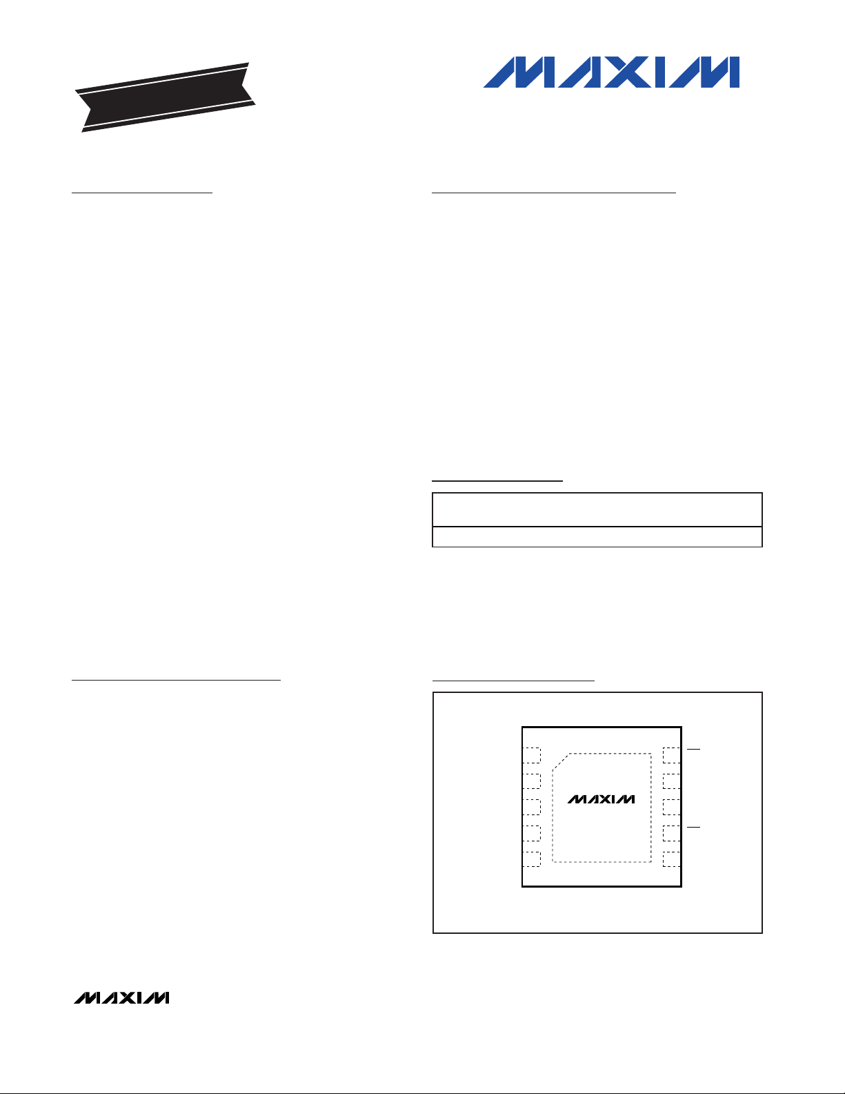
Pin Configuration
Ordering Information
19-3975; Rev 0; 4/06
For pricing, delivery, and ordering information, please contact Maxim/Dallas Direct! at
1-888-629-4642, or visit Maxim’s website at www.maxim-ic.com.
PART PIN-PACKAGE
PKG
CODE
MAX6603ATB+ 10 TDFN-EP*
T1033-1
EVALUATION KIT
AVAILABLE
Note: Device is specified over the -40°C to +125°C tempera-
ture range.
*EP = Exposed pad.
+Denotes lead-free package.
**Other base resistance values can be accommodated.
Contact the factory for more information.
RTD
200Ω**
Page 2
MAX6603
Dual-Channel, Platinum RTD-to-Voltage
Signal Conditioner
2 _______________________________________________________________________________________
ABSOLUTE MAXIMUM RATINGS
ELECTRICAL CHARACTERISTICS
(VCC= 3.0V to 5.5V, resistor connected between RS1+ and RS1- = 560Ω, resistor connected between RS2+ and RS2- = 560Ω,
T
A
= -40°C to +125°C, unless otherwise noted. Typical values are at VCC= 5.0V, RL= 47kΩ between OUT_ and GND, TA= +25°C.)
(Note 1)
Stresses beyond those listed under “Absolute Maximum Ratings” may cause permanent damage to the device. These are stress ratings only, and functional
operation of the device at these or any other conditions beyond those indicated in the operational sections of the specifications is not implied. Exposure to
absolute maximum rating conditions for extended periods may affect device reliability.
(All voltages referenced to GND, unless otherwise noted.)
V
CC
........................................................................-0.3V to +6.0V
RS1+, RS1-, RS2+, RS2- .....................................-0.3V to +18.0V
OUT1, OUT2, DG1, DG2 ............................-0.3V to (V
CC
+ 0.3V)
Continuous Power Dissipation (T
A
= +70°C)
10-Pin TDFN Single-Layer Board
(derate 18.5 mW/°C above +70°C).........................1481.5mW
10-Pin TDFN Multilayer Board
(derate 24.4 mW/°C above +70°C).........................1951.2mW
ESD Protection (OUT1, OUT2, DG1, DG2,
Human Body Model) .....................................................> ±2kV
ESD Protection (RS1+, RS2+, RS1-, RS2-,
V
CC
, GND, Human Body Model) ..................................> ±5kV
Operating Temperature Range .........................-40°C to +125°C
Junction Temperature......................................................+150°C
Storage Temperature Range .............................-65°C to +150°C
Lead Temperature (soldering, 10s) .................................+300°C
PARAMETER
SYMBOL
CONDITIONS
MIN
TYP
MAX
UNITS
Supply Voltage V
CC
3.0 5.5 V
Input Over Voltage V
RS
RS1+, RS1-, RS2+, RS2- 16 V
3.9 5.5
Supply Current I
CC
Sink current during overvoltage fault
mA
CURRENT SOURCES
Excitation Current I
EXC
(Note 2)
1.0
mA
Excitation-Current Temperature
Coefficient
TCI
EXC
(Note 2) -7
ppm/°C
Minimum RS_- Voltage V
RS_-
3.4 V
Maximum RS_+ Voltage V
RS_+
4.0 V
Supply Ratiometric I
RATIO
VCC = +3V to +5.5V 0.2
mA/V
MAXIMUM TEMPERATURE ERROR (Note 3)
+400°C to +600°C, VCC = 5.0V ±6
-40°C to +400°C, VCC = 5.0V ±8
+600°C to +1000°C, VCC = 5.0V ±12
+400°C to +600°C, VCC = 3.0V ±10
-40°C to +400°C, VCC = 3.0V
RTD
+600°C to +1000°C, VCC = 3.0V ±20
°C
V
= V
RS1+
RS1 -
= V
RS2+
= V
= +16V
RS2-
0.58
36.2 47.1
1.12
±13.3
Page 3
MAX6603
Dual-Channel, Platinum RTD-to-Voltage
Signal Conditioner
_______________________________________________________________________________________ 3
Note 1: All parameters are tested at TA= +25°C. Specifications over temperature are guaranteed by design.
Note 2: RTD resistance range is 150Ω to 900Ω for constant excitation current.
Note 3: A typical 200Ω RTD: R(T) = R
O
[1 + AT + BT2] is referenced for probe temperature-probe resistance relation. The parame-
ters in this section are not tested and are for reference only.
Note 4: RTD resistance is tested only at R
RTD
= 200Ω, 560Ω, 845Ω. The range is guaranteed by design.
Note 5: Parameters are tested in special test mode.
ELECTRICAL CHARACTERISTICS (continued)
(VCC= 3.0V to 5.5V, resistor connected between RS1+ and RS1- = 560Ω, resistor connected between RS2+ and RS2- = 560Ω,
T
A
= -40°C to +125°C, unless otherwise noted. Typical values are at VCC= 5.0V, RL= 47kΩ between OUT_ and GND, TA= +25°C.)
(Note 1)
PARAMETER
SYMBOL
CONDITIONS
MIN
TYP
MAX
UNITS
MAXIMUM INPUT RESISTANCE-TO-OUTPUT VOLTAGE ERROR
494Ω to 627Ω, VCC = 5.0V 19
200Ω to 494Ω, VCC = 5.0V 27
627Ω to 866Ω, VCC = 5.0V 33
494Ω to 627Ω, VCC = 3.0V 19
200Ω to 494Ω, VCC = 3.0V 27
RTD (Note 4)
627Ω to 866Ω, VCC = 3.0V 33
mV
ANALOG OUTPUTS (OUT1, OUT2)
Output-Voltage Low (Max) V
OL
RL = 47kΩ between OUT_ and V
CC
(Note 5)
0.1 V
Output-Voltage High (Min) V
OH
RL = 47kΩ between OUT_ and GND
(Note 5)
VCC -
0.1
V
V
OUT
= V
CC
22 mA
Short-Circuit Current I
SC
V
OUT
= GND 12 mA
Maximum Capacitive Load C
L
500 pF
Minimum Resistive Load R
L
Between OUT_ and GND 20 kΩ
DIAGNOSTIC OUTPUTS (DG1, DG2)
Output-Voltage Low V
OL
I
SOURCE
= 1mA 0.2 V
Output-Voltage High V
OH
I
SINK
= 1mA
V
CC
-
0.2
V
Minimum Resistance for RS+,
RS - Open
Ω
Maximum Resistance for RS+,
RS - Short
60 Ω
R
RS - OPEN
R
RS - SHORT
8000
Page 4

MAX6603
Dual-Channel, Platinum RTD-to-Voltage
Signal Conditioner
4 _______________________________________________________________________________________
Typical Operating Characteristics
(VCC= 5.0V, TA= +25°C, unless otherwise noted.)
2.0
2.6
2.3
3.2
2.9
3.5
3.8
3.0 5.5
SUPPLY CURRENT
vs. SUPPLY VOLTAGE
MAX6603 toc01
SUPPLY VOLTAGE (V)
SUPPLY CURRENT (mA)
4.03.5 4.5 5.0
TA = -40°C
TA = 0°C
TA = +125°C
TA = +85°C
TA = +25°C
-20
10
0
-10
20
-40 -10 20 50 80 110
OUTPUT-VOLTAGE DRIFT
vs. TEMPERATURE
MAX6603 toc02
TEMPERATURE (°C)
OUTPUT-VOLTAGE DRIFT (mV)
POWER-SUPPLY REJECTION RATIO
vs. FREQUENCY
MAX6603 toc03
FREQUENCY (kHz)
PSRR (dB)
100.0010.001.000.10
-90
-80
-70
-60
-50
-40
-30
-20
-10
0
-100
0.01 1000.00
0
1
3
2
4
5
OUTPUT VOLTAGE
vs. RTD RESISTANCE
MAX6603 toc04
RTD RESISTANCE (Ω)
OUTPUT VOLTAGE (V)
100 500300 700 900
TA = 25°C
Page 5

MAX6603
Dual-Channel, Platinum RTD-to-Voltage
Signal Conditioner
_______________________________________________________________________________________ 5
Detailed Description
The MAX6603 converts a Deutsche Institute for Normung
(DIN) standard 200Ω Pt RTD to a high-level analog voltage without the need for external trims or precise discrete components. The Pt RTD resistance conveys
temperature information approximated by the CallendarVan Dusen equation and is represented in Figure 1:
R(T) = R
O
[1 + AT + BT2+ CT3]
where: R(T) = Resistance of Pt RTD at temperature (T)
R0= Base resistance in ohms at 0°C
T = Temperature in °C
A = 3.9083 E-3 °C-1(alpha coefficient 1)
B = -5.7750 E-7 °C
-2
(alpha coefficient 2)
C = 0 (approximation for temperatures > 0°C)
(Alpha coefficients can vary depending on
standards.)
The MAX6603 applies a constant excitation current of
1mA (typ) through the Pt RTD, generating a voltage
drop that is amplified and results in a high-level output
voltage. The excitation current (I
EXC
) typically varies
ratiometrically by 0.2mA/V (typ) with respect to VCC,
and therefore, the amplified signal is ratiometric to the
power supply. The voltage amplification from input to
output is 5 (typ). The output voltage is applied to a
ratiometric ADC to produce a digital value independent
of supply voltage. For ADCs that use VCCas their reference voltage, sudden changes in the supply voltage do
not affect the microcontroller’s reading of the temperature. Ratiometricity simplifies the connection to most
Pin Description
PIN NAME FUNCTION
1VCCPower-Supply Input. Bypass to GND with a 0.1µF capacitor as close to VCC as possible.
2 RS2- Sense Resistor 2 Negative Input
3 RS2+ Sense Resistor 2 Positive Input
4 RS1+ Sense Resistor 1 Positive Input
5 RS1- Sense Resistor 1 Negative Input
6 GND Ground
7 DG1 Diagnostic Output Signal 1. DG1 asserts low upon fault detection.
8 OUT1 Output Analog Voltage 1. OUT1 is high impedance upon DG1 assertion.
9 OUT2 Output Analog Voltage 2. OUT2 is high impedance upon DG2 assertion.
10 DG2 Diagnostic Output Signal 2. DG2 asserts low upon fault detection.
—EPExposed Pad. Connect to GND.
Functional Block Diagram
MAX6603
RS1+
RS1-
OUT1
AMP
FAULT
DETECT
DG1
HI-V
DETECT
I
EXC
ESD
CLAMP
ESD
CLAMP
V
CC
R
SRC
RS2+
RS2-
OUT2
AMP
FAULT
DETECT
DG2
HI-V
DETECT
I
EXC
ESD
CLAMP
ESD
CLAMP
V
CC
R
SRC
V
CC
GND
Page 6

MAX6603
Dual-Channel, Platinum RTD-to-Voltage
Signal Conditioner
6 _______________________________________________________________________________________
microcontrollers that incorporate an ADC and enables a
low-cost, low-complexity solution. Ratiometricity is an
important consideration for battery-operated instruments, automotive, and some industrial applications.
Temperature Information
The MAX6603 measures the resistance between the
RTD and translates that into a high-level output voltage.
The resistance range of the MAX6603 is between 150Ω
and 900Ω, covering a -40°C to +1000°C temperature
range. When R(T) goes too low or too high, a fault condition is asserted and the respective DG_ goes low.
Output Voltage
The following equation describes the output voltage:
where:
VCC= supply voltage
R(T) = RTD resistance given by CallendarVan Dusen equation.
Using Other Pt RTDs
The MAX6603 is designed for a 200Ω Pt RTD, but the
device can work with any RTD as long as the resistance
is in the 150Ω to 900Ω range. A 500Ω Pt RTD can be
used for temperatures up to +208°C because that tem-
perature results in R(T) = 900Ω.
Input Overvoltage Protection to +16V
The input pins RS1+, RS1-, RS2+, and RS2- protect the
MAX6603 from overvoltage conditions up to +16V without damaging the device.
Diagnostic Outputs (
DG1, DG2
)
The MAX6603 continuously monitors the excitation
current to the RTD, the resultant voltage drop, and
voltage levels of the inputs to detect fault conditions.
Any fault condition causes the respective DG output to
assert low. Fault conditions occur for RTD open circuits;
RTD short circuits; and RS1+, RS1-, RS2+, and RS2short to ground or supply. If any fault is detected, the
respective DG output asserts low. OUT1 and OUT2 are
high impedance on assertion of DG1 and DG2, respec-
tively. An example circuit showing potential fault conditions is shown in Figure 2.
Applications Information
Ratiometric Output Coupled to a
Microcontroller
The circuit of Figure 3 shows the MAX6603 connected to
the microcontroller using V
CC
as the ADC reference voltage. The output is ratiometric to VCC, and temperature
measurements are independent of the supply voltage.
Chip Information
PROCESS: BiCMOS
V
VR
1
OUT
CC
=
× ()T
000
0
300
200
100
400
500
600
700
800
900
1000
0 400200 600 800 1000
200Ω Pt RTD
TEMPERATURE (°C)
RESISTANCE (Ω)
Figure 1. Typical 200Ω Pt RTD Representation by the
Simplified Callender-Van Dusen Equation
Page 7

MAX6603
Dual-Channel, Platinum RTD-to-Voltage
Signal Conditioner
_______________________________________________________________________________________ 7
MAX6603
RS1+
RS1-
OUT1
AMP
FAULT
DETECT
DG1
HI-V
DETECT
I
EXC
ESD
CLAMP
ESD
CLAMP
V
CC
R
SRC
RS2+
RS2-
OUT2
AMP
FAULT
DETECT
DG2
HI-V
DETECT
I
EXC
ESD
CLAMP
ESD
CLAMP
V
CC
R
SRC
V
CC
GND
0.1µF 0.1µF
OUT1
ADC2
INPUT2
ADC1
INPUT1
+5V
V
CC
ADC-REF
±5kV ESD
SHORT TOGETHEROPEN
OPEN
SHORT TO BAT
(16V)
SHORT TO BAT
(16V)
SHORT TO GND
SHORT TO GND
RTD SENSOR
CHASSIS GND
MICROCONTROLLER
Figure 2. The various fault conditions that cause the diagnostic output to assert low are shown for a single channel.
Page 8

MAX6603
Dual-Channel, Platinum RTD-to-Voltage
Signal Conditioner
8 _______________________________________________________________________________________
MAX6603
RS1+
RS1-
RS2+
RS2-
OUT1
AMP
FAULT
DETECT
DG1
HI-V
DETECT
I
EXC
ESD
CLAMP
ESD
CLAMP
V
CC
R
SRC
OUT2
AMP
FAULT
DETECT
DG2
HI-V
DETECT
I
EXC
ESD
CLAMP
ESD
CLAMP
V
CC
R
SRC
V
CC
GND
0.1µF 0.1µF
OUT1
ADC2
INPUT2
ADC1
INPUT1
+5V
ADC-REF
MICROCONTROLLER
Pt RTD PROBE
Pt RTD PROBE
CONNECTOR
CONNECTOR
Figure 3. A Typical Application Circuit with Ratiometric Output Coupled to Ratiometric Microcontroller ADC
Page 9

MAX6603
Dual-Channel, Platinum RTD-to-Voltage
Signal Conditioner
Maxim cannot assume responsibility for use of any circuitry other than circuitry entirely embodied in a Maxim product. No circuit patent licenses are
implied. Maxim reserves the right to change the circuitry and specifications without notice at any time.
Maxim Integrated Products, 120 San Gabriel Drive, Sunnyvale, CA 94086 408-737-7600 _____________________ 9
© 2006 Maxim Integrated Products Printed USA is a registered trademark of Maxim Integrated Products, Inc.
6, 8, &10L, DFN THIN.EPS
COMMON DIMENSIONS
SYMBOL MIN. MAX.
A 0.70 0.80
D 2.90 3.10
E 2.90 3.10
A1 0.00 0.05
L 0.20 0.40
PKG. CODE N D2 E2 e JEDEC SPEC b
[(N/2)-1] x e
PACKAGE VARIATIONS
0.25 MIN.k
A2 0.20 REF.
2.00 REF0.25±0.050.50 BSC2.30±0.1010T1033-1
2.40 REF0.20±0.05- - - - 0.40 BSC1.70±0.10 2.30±0.1014T1433-1
1.50±0.10 MO229 / WEED-3
0.40 BSC - - - - 0.20±0.05 2.40 REFT1433-2 14 2.30±0.101.70±0.10
T633-2 6 1.50±0.10 2.30±0.10 0.95 BSC MO229 / WEEA 0.40±0.05 1.90 REF
T833-2 8 1.50±0.10 2.30±0.10 0.65 BSC MO229 / WEEC 0.30±0.05 1.95 REF
T833-3 8 1.50±0.10 2.30±0.10 0.65 BSC MO229 / WEEC 0.30±0.05 1.95 REF
2.30±0.10 MO229 / WEED-3 2.00 REF0.25±0.050.50 BSC1.50±0.1010T1033-2
Package Information
(The package drawing(s) in this data sheet may not reflect the most current specifications. For the latest package outline information,
go to www.maxim-ic.com/packages
.)
 Loading...