

Page 1
General Description
The MAX6513 is a fully integrated, remote temperature
switch that uses an external P-N junction (typically a
diode-connected transistor) as the sensing element to
measure the remote temperature. The device asserts a
logic signal when the temperature crosses a factoryprogrammed threshold. Available trip thresholds are
from +45°C to +125°C in 10°C increments. Accuracy is
within ±3°C (T
A
= -5°C to +55°C) or ±5°C (TA= -40°C
to +85°C). Hysteresis is pin selectable to 5°C or 10°C.
The MAX6513 has an active-high CMOS output. The
output is asserted when the temperature exceeds the
threshold value. The active-high CMOS output can
directly drive a power FET to control a cooling fan.
The MAX6513 operates from a +3.0V to +5.5V supply
and typically consumes 400µA of supply current. It is
available in a 6-pin lead-free TDFN package.
Applications
CPU Temperature Monitoring in High-Speed
Computers
Multichip Modules
Battery Packs
Temperature Control
Temperature Alarms
Fan Control
Features
♦ Continuously Measure External Junction
Temperature
♦ Factory-Programmed Temperature Threshold
from +45°C to +125°C in 10°C Increments
♦ Insensitive to Series Parasitic Resistance
♦ Active-High Output for Direct Fan Control
♦ < 100ms Response Time
♦ Accuracy
±3°C (T
REMOTE
=
+45°C to +125°C, T
A
= -5°C to +55°C)
±5°C (T
REMOTE
=
+45°C to +125°C, T
A
= -40°C to +85°C)
♦ Pin-Selectable 5°C or 10°C Hysteresis
♦ 400µA Average Current Consumption
♦ +3.0V to +5.5V Supply Range
♦ 6-Pin TDFN Package (Lead(Pb)-Free) with
Exposed Pad
MAX6513
Low-Cost, Remote Temperature Switch
________________________________________________________________
Maxim Integrated Products
1
19-1819; Rev 3; 2/11
Ordering Information
Note: These parts are offered in nine standard temperature
versions with a minimum order of 2500 pieces. To complete
the suffix information, select an available trip point in degrees
centigrade from the device marking codes table. For example,
the MAX6513TT065+T describes a MAX6513 in a 6-pin TDFN
package with a +65°C threshold.
+
Denotes a lead(Pb)-free/RoHS-compliant package.
T = Tape and reel.
*
EP = Exposed pad.
For pricing, delivery, and ordering information, please contact Maxim Direct at 1-888-629-4642,
or visit Maxim’s website at www.maxim-ic.com.
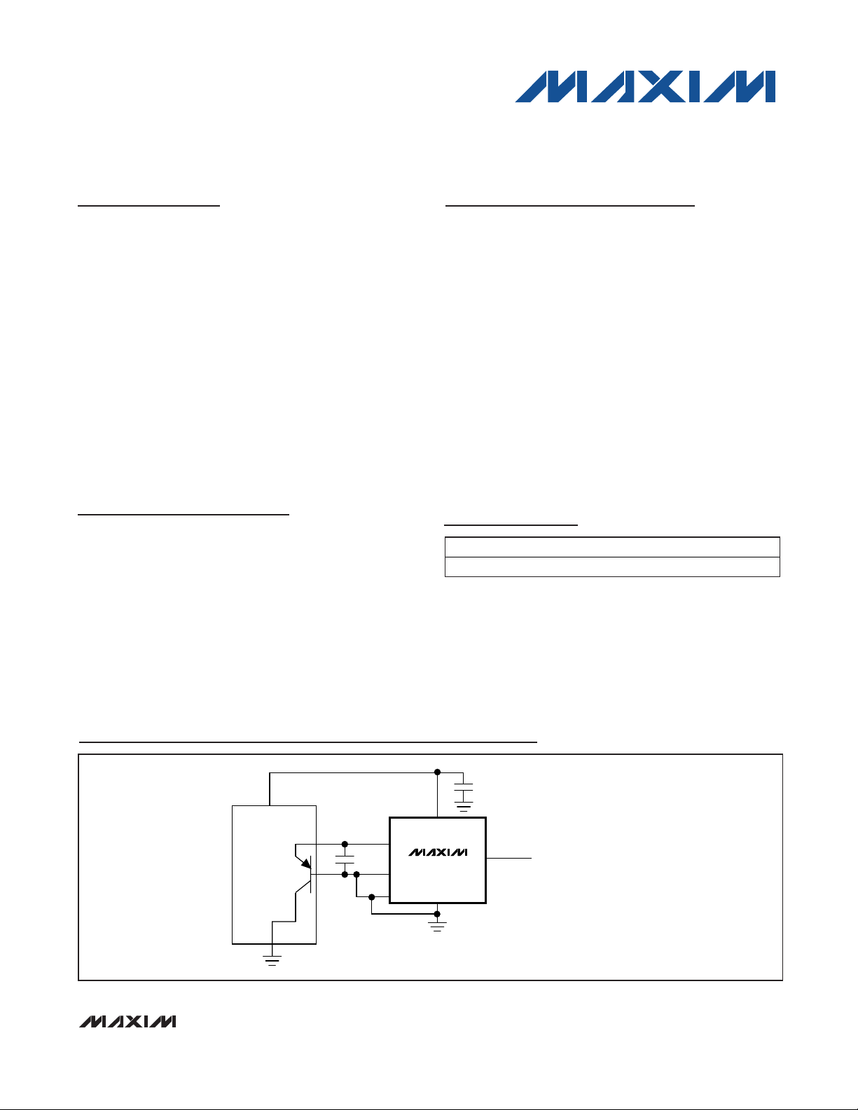
Typical Operating Circuit
PART TEMP RANGE PIN-PACKAGE
MAX6513TT_ _ _ +T -40°C to +85°C 6 TDFN-EP*
3.3V
V
DD
μP
C
DXP
S
DXN
HYST
MAX6513
2μF
TOVER (TO MICROPROCESSOR FAN
CONTROLLER, SHUTDOWN, ETC.)
Page 2
MAX6513
Low-Cost, Remote Temperature Switch
2 _______________________________________________________________________________________
ABSOLUTE MAXIMUM RATINGS
ELECTRICAL CHARACTERISTICS
(V
DD
= +3.0V to +5.5V, CS= 2200pF, TA= -40°C to +85°C, T
REMOTE
= +45°C to +125°C (Note 1), unless otherwise noted. Typical
values are at T
A
= +25°C.) (Note 2)
Stresses beyond those listed under “Absolute Maximum Ratings” may cause permanent damage to the device. These are stress ratings only, and functional
operation of the device at these or any other conditions beyond those indicated in the operational sections of the specifications is not implied. Exposure to
absolute maximum rating conditions for extended periods may affect device reliability.
Note 1: T
REMOTE
refers to the temperature of the remote-sensing junction. TArefers to the temperature of the MAX6513 package.
Note 2: All parameters are 100% production tested at T
A
= +25°C. Specifications over temperature limits are guaranteed by design.
Note 3: This parameter is guaranteed by design to ±3.5 sigma.
Supply Voltage (V
DD
) ...............................................-0.3V to +6V
DXP, DXN, HYST, TOVER...........................-0.3V to (V
DD
+ 0.3V)
TOVER Output Current............................................-1mA/+50mA
DXN Input Current...................................................-1mA/+50mA
Current (all other pins)......................................................±20mA
Continuous Power Dissipation (T
A
= +70°C)
TDFN (derate 18.2mW/°C above +70°C)...................1455mW
Operating Temperature Range ...........................-40°C to +85°C
Storage Temperature Range .............................-65°C to +150°C
Junction Temperature......................................................+150°C
Lead Temperature (soldering, 10s) .................................+300°C
Soldering Temperature ....................................................+260°C
PARAMETER S YMBOL CONDITIONS MIN TYP MAX UNITS
Supply Voltage Range V
Supply Current I
Temperature Threshold
Accuracy (Note 3)
Power-Supply Sensitivit y for
Temperature Trip Point
Temperature Threshold
Hysteresis
Response Time 70 120 ms
Input Voltage High V
Input Voltage Low V
Output Voltage High V
Output Voltage Low V
Maximum DXP Source
Current
Minimum DXP Source
Current
DD
DD
T
TH
T
HYST
IH
IL
OH
OL
3.0 5.5 V
400 600 μA
TA = -5°C to +55°C -3.0 +3.0
TA = -40°C to +85°C -5.0 +5.0
HYST = V
HYST = V
0.2 V
I
OUT
I
OUT
0.4V V
DXN = GND
0.4V V
DXN = GND
IL
IH
= 1mA
= 1mA 0.2 V
2V,
DXP
2V,
DXP
-0.6 °C/V
5
10
VDD -
0.2
V
DD
0.2
270 μA
9 μA
V
V
°C
°C
Page 3

MAX6513
Low-Cost, Remote Temperature Switch
_______________________________________________________________________________________
3
Typical Operating Characteristics
(VDD= +3.3V, CS= 2200pF, TA= +25°C, unless otherwise noted.)
SUPPLY CURRENT
vs. AMBIENT TEMPERATURE
440
420
400
380
360
SUPPLY CURRENT (μA)
340
320
300
-40 10-15 35 60 85
AMBIENT TEMPERATURE TA (°C)
(NOTE: SUPPLY CURRENT
INCLUDES EXTERNAL
DIODE-CONNECTED
TRANSISTOR)
MAX6511 toc01
TEMPERATURE TRIP THRESHOLD ERROR
vs. AMBIENT TEMPERATURE T
0.2
0
-0.2
-0.4
-0.6
-0.8
-1.0
-1.2
-1.4
TEMPERATURE TRIP THRESHOLD ERROR (°C)
-1.6
-60 -40 -20 0 20 40 8060 100 120 140
AMBIENT TEMPERATURE TA (°C)
TEMPERATURE TRIP THRESHOLD ERROR
vs. SERIES RESISTANCE
1.0
0.5
0
-0.5
-1.0
-1.5
TEMPERATURE TRIP THRESHOLD ERROR (°C)
-2.0
0806020 40 100 120 140 160 180 200
SERIES RESISTANCE (Ω)
MAX6511 toc04
TEMPERATURE TRIP THRESHOLD ERROR
A
MAX6511 toc02
14
12
10
8
6
4
2
0
-2
TEMPERATURE TRIP THRESHOLD ERROR (°C)
-4
02010 30 40 50 60
TEMPERATURE TRIP THRESHOLD
vs. SUPPLY VOLTAGE
0.4
0.2
0
-0.2
-0.4
-0.6
-0.8
-1.0
-1.2
-1.4
-1.6
TEMPERATURE TRIP THRESHOLD ERROR (°C)
-1.8
3.0 4.03.5 4.5 5.0 5.5
SUPPLY VOLTAGE (V)
CAPACITANCE
vs. C
S
CS CAPACITANCE (nF)
MAX6511 toc05
MAX6511 toc03
Page 4

Detailed Description
The MAX6513 fully integrated temperature switch incorporates a precision bandgap reference, a conversion
block, a current source, and a comparator (Figure 1).
The device uses an external P-N junction as the temperature-sensing element. It steers bias currents
through the external diode, measures the forward voltages, and computes the temperature using a precision
chopper stabilized amplifier.
Resistance values of less than 100Ω in series with the
external sense junction will result in trip-point errors
< 1°C. The MAX6513 provides noise immunity by integration and oversampling of the diode voltage, but
good design practice includes routing the DXP and
DXN lines away from noise sources, such as highspeed digital lines, switching regulators, inductors, and
transformers. The DXP and DXN traces should be
paired together and surrounded by ground plane
whenever possible.
In applications where the temperature changes rapidly,
the measured temperature will be approximately equal
to the average value of the temperature during the
measurement period.
The MAX6513 has an active-high CMOS output, and is
available with preset temperature thresholds from
+45°C to +125°C in 10°C increments.
MAX6513
Low-Cost, Remote Temperature Switch
4 _______________________________________________________________________________________
Pin Description
Figure 1. Functional Block Diagram
GND
TOVERHYST
16DXP
+
5 DXN
V
DD
MAX6513
TOP VIEW
2
34
TDFN
EP
Pin Configuration
PIN NAME FUNCTION
1 V
2 GND Ground
3 HYST
4 TOVER
5 DXN
6 DXP
— EP
DD
Power-Supply Input, +3.0V to
+5.5V. Bypass V
a 0.1μF capacitor.
Hysteresis Select ion. Hystere sis
is 10°C for HYST = VDD, 5°C for
HYST = GND.
CMOS Active-High Output.
TOVER goes high when the
temperature exceeds the factoryprogrammed temperature
threshold.
This pin connects to the
negative (cathode) terminal of
the external P-N sense junction.
DXN must be connected to GND.
This pin connects to the positive
(anode) terminal of the external
P-N sense junction.
Exposed Pad. Not internally
connected. Connect to GND or
leave unconnected.
to GND with
DD
DXP
DXN
BANDGAP
TEMPERATURE
CONVERSION
VOLTAGE
REFERENCE
COMPAR-
ATOR
LATCH
TOVER
Page 5

Hysteresis Input
The HYST pin is a CMOS-compatible input that selects
hysteresis at either a high level (10°C for HYST = VDD)
or a low level (5°C for HYST = GND). Hysteresis prevents the output from chattering when the temperature
is near the trip point. The HYST pin must not be left
unconnected.
The output asserts when the temperature exceeds the
trip point and deasserts when the temperature falls
back below the trip point minus the hysteresis. For
example, if the trip point is 105°C, the output will assert
at 105°C and will not deassert until temperature falls
below 105°C minus the hysteresis (e.g., 95°C if 10°C
hysteresis is chosen) (Figure 2).
Applications Information
Remote-Diode Selection
To ensure best accuracy, use a good-quality diodeconnected transistor. Suggested devices are listed in
Table 1. Large power transistors are not recommended. Tight specifications for forward current gain indicate the manufacturer has good process controls and
that the devices have consistent Vbecharacteristics.
The MAX6513 can also measure the die temperature of
CPUs and other integrated circuits having on-board
temperature-sensing diodes. Use the monitor’s output
to reset the µP, assert an interrupt, activate a cooling
fan, or trigger an external alarm.
Noise Filtering Capacitors
A quality ceramic capacitor must be connected across
the DXP/DXN inputs to maintain temperature threshold
accuracy by filtering out noise. The capacitor should
be located physically close to the DXP/DXN pins and
should typically have a value of 2200pF. Larger capacitor values can cause temperature measurement errors.
A 50% variation from the recommended capacitor
value can cause up to ±1°C error.
MAX6513
Low-Cost, Remote Temperature Switch
_______________________________________________________________________________________ 5
Figure 2. Temperature Trip Threshold Hysteresis
Table 1. Sensor Transistor Manufacturers
Note: Transistors must be diode connected (base shorted to
collector).
Device Marking Codes
for TDFN Package
Package Information
For the latest package outline information and land patterns
(footprints), go to www.maxim-ic.com/packages
. Note that a
“+”, “#”, or “-” in the package code indicates RoHS status only.
Package drawings may show a different suffix character, but
the drawing pertains to the package regardless of RoHS status.
PACKAGE
TYPE
PACKAGE
CODE
OUTLINE
NO.
LAND
PATTERN NO.
6 TDFN-EP T633+2
21-0137 90-0058
MANUFACTURER MODEL NUMBER
Central Semiconductor (USA) CMPT3904
ON (USA) MMBT3904
Rohm Semiconductor (Japan) SST3904
Samsung (Korea) KST3904-TF
Siemens (Germany) SMBT3904
Zetex (England) FMMT3904CT-ND
TRIP TEMPERATURE
TRIP TEMPERATURE HYSTERESIS
TOVER
TIME
DEVICE CODE
MAX6513TT045 +ACU 45
MAX6513TT055 +ACV 55
MAX6513TT065 +ACW 65
MAX6513TT075 +ACX 75
MAX6513TT085 +ACY 85
MAX6513TT095 +ACZ 95
MAX6513TT105 + ADA 105
MAX6513TT115 + ADB 115
MAX6513TT125 + ADC 125
TEMPERATURE TRIP
THRESHOLD (°C)
Page 6

MAX6513
Low-Cost, Remote Temperature Switch
Maxim cannot assume responsibility for use of any circuitry other than circuitry entirely embodied in a Maxim product. No circuit patent licenses are
implied. Maxim reserves the right to change the circuitry and specifications without notice at any time.
6
_____________________Maxim Integrated Products, 120 San Gabriel Drive, Sunnyvale, CA 94086 408-737-7600
© 2011 Maxim Integrated Products Maxim is a registered trademark of Maxim Integrated Products, Inc.
Revision History
REVISION
NUMBER
2 10/04
3 2/11
REVISION
DATE
DESCRIPTION
Added the TDFN package to the General De scr iption, Features, Pin Configuration,
Ordering Information, and Absolute Maximum Ratings sect ions; added TDFN top mark
codes to the Device Marking Codes for SOT23-6 Package table; added the TDFN
package outl ine drawing
Removed the MAX6511/MAX6512 parts and SOT23 package s from the data sheet;
changed the leaded part to lead(Pb)-free in the Ordering Information table; in the
Absolute Maximum Ratings section changed the continuous power dissipation
numbers (24.4mW/°C to 18.2mW/°C and 1951mW to 1455mW), added the soldering
temperature, and updated the lead temperature; added the exposed pad description to
the Pin Description table; removed the top mar ks for SOT23-6 packages from the
Device Marking Codes for SOT23-6 Package table and renamed the table; removed
the Chip Information section; added the Pac kage Information table
PAGES
CHANGED
1, 2, 6, 8
1–6
 Loading...