

Page 1
General Description
The MAX6505–MAX6508 temperature switches have dual
logic outputs that assert when the die temperature crosses their trip thresholds. Trip thresholds are factory programmed to convenient temperatures in 5°C increments.
The MAX6505/MAX6506 have an ALARM output that
asserts when the temperature is above the factory-programmed thresholds (available from -40°C to +125°C).
They also have a WARN output that asserts when the
temperature is several degrees below the ALARM threshold. The difference between the ALARM and WARN
thresholds (ΔT
AW
) is pin selectable to +5°C, +10°C,
+20°C, or +30°C. The MAX6505’s logic outputs are open
drain, while the MAX6506’s logic outputs are push-pull.
The MAX6507 has open-drain outputs (OVER, OK), and
the MAX6508 has push-pull outputs (OVER, OK), each
with two factory-programmed threshold temperatures
(T
OVER
and T
UNDER
) in the wide range of -40°C to
+125°C. The overtemperature output asserts when the
temperature is above T
OVER
. When the temperature is in
the desired window (less than T
OVER
and greater than
T
UNDER
), OK (OK) asserts.
The MAX6505–MAX6508 are accurate to ±0.5°C (typ),
±5.5°C (max). Operating from a +2.5V to +5.5V supply,
these low-cost devices typically consume 30µA supply
current and require no external components for setting
trip points. The MAX6505–MAX6508 are available in a
6-pin SOT23 package.
________________________Applications
µP Temperature Monitoring in High-Speed
Computers
Temperature Control
Temperature Alarms
Fan Control
Features
♦ ±0.5°C (typ) Threshold Accuracy Over Full
Temperature Range
♦ No External Components Required
♦ Low Cost
♦ 30µA (typ) Supply Current
♦ Factory-Programmed Thresholds from -40°C to
+125°C in 5°C Increments
♦ Open-Drain Outputs (MAX6505/MAX6507),
Push-Pull Outputs (MAX6506/MAX6508)
♦ Pin Selectable 2°C, 10°C Hysteresis
(MAX6507/MAX6508)
♦ Pin Selectable +5°C, +10°C, +20°C, +30°C
T
ALARM
- T
WARN
(MAX6505/MAX6506)
♦ SOT23 Package
Note: To complete the suffix information for the MAX6505/
MAX6506, add P or N for positive or negative trip temperature, and select an available trip point in degrees centigrade.
For example, the MAX6505UTP055+T describes a MAX6505 in
a SOT23 package with a +55°C threshold (Table 3). Contact
the factory for pricing and availability of temperature versions
(minimum order 10,000 pieces).
To complete the suffix information for MAX6507/MAX6508, see
Table 4.
+
Denotes a lead(Pb)-free/RoHS-compliant package.
T = Tape and reel.
MAX6505–MAX6508
Dual Trip SOT Temperature Switches
________________________________________________________________
Maxim Integrated Products
1
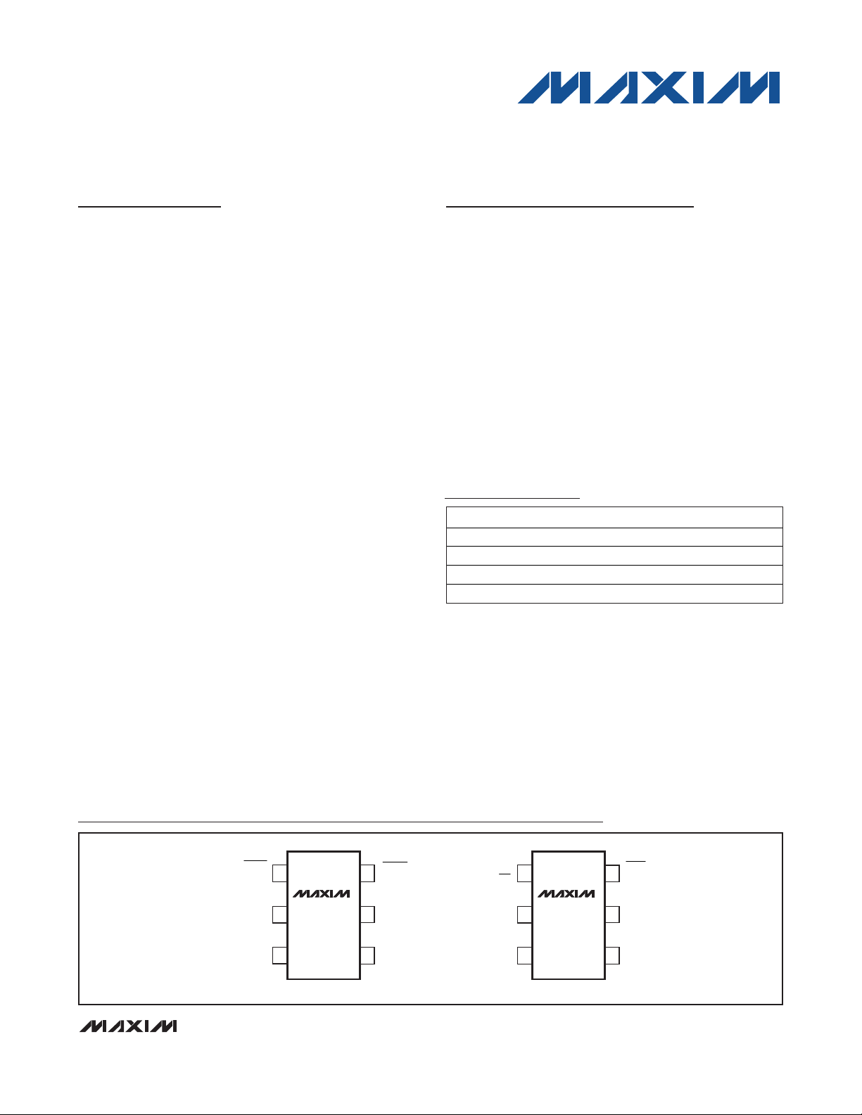
Pin Configurations
19-1712; Rev 1; 2/11
For pricing, delivery, and ordering information, please contact Maxim Direct at 1-888-629-4642,
or visit Maxim’s website at www.maxim-ic.com.
Ordering Information
Selector Guide appears at end of data sheet.
Typical Operating Circuits appear at end of data sheet.
PART TEMP RANGE PIN-PACKAGE
MAX6505UT_ _ _ _+T
MAX6506UT_ _ _ _+T
MAX6507UT_ _ _ _+T
MAX6508UT_ _ _ _+T -40°C to +125°C 6 SOT23
-40°C to +125°C 6 SOT23
-40°C to +125°C 6 SOT23
-40°C to +125°C 6 SOT23
TOP VIEW
WARN
(WARN)
GND
( ) ARE FOR MAX6506.
+
16
MAX6505
2
MAX6506
S1
34
SOT23
5 S0
ALARM
(ALARM)
V
CC
+
OK
16
(OK)
GND
S0
MAX6507
2
MAX6508
34
SOT23
OVER
(OVER)
5 N.C.
V
CC
( ) ARE FOR MAX6508.
Page 2
MAX6505–MAX6508
Dual Trip SOT Temperature Switches
2 _______________________________________________________________________________________
ABSOLUTE MAXIMUM RATINGS
ELECTRICAL CHARACTERISTICS
(VCC= +2.5V to +5.5V, R
PULLUP
= 100kΩ (MAX6505/MAX6507 only), TA= -40°C to +125°C, unless otherwise noted. Typical values
are at T
A
= +25°C and VCC= +5V, unless otherwise noted.) (Note 1)
Stresses beyond those listed under “Absolute Maximum Ratings” may cause permanent damage to the device. These are stress ratings only, and functional
operation of the device at these or any other conditions beyond those indicated in the operational sections of the specifications is not implied. Exposure to
absolute maximum rating conditions for extended periods may affect device reliability.
Supply Voltage (VCCto GND) ..................................-0.3V to +6V
S1, S0 to GND ............................................-0.3V to (V
CC
+ 0.3V)
All Other Pins to GND.................................-0.3V to (V
CC
+ 0.3V)
Input/Output Current, All Pins...........................................±20mA
Continuous Power Dissipation (T
A
= +70°C)
SOT23 (derate 8.7mW/°C above +70°C)....................696mW
Operating Temperature Range (T
MIN
to T
MAX
) ..-40°C to +125°C
Thermal Resistance (θ
JA
)...............................................115°C/W
Storage Temperature Range .............................-65°C to +150°C
Maximum Die Temperature..............................................+150°C
Lead Temperature (soldering, 10s) .................................+300°C
Soldering Temperature (reflow) .......................................+260°C
PARAMETER SYMBOL CONDITIONS MIN TYP MAX UNITS
Supply Voltage Range V
Supply Current I
Temperature Threshold
Accuracy (Note 2)
Delta Temperature
ALARM
-T
WARNING
(T
MAX6505/MAX6506
Temperature Threshold
Hysteresis (Note 3)
)
CC
S0 = S1 = GND
CC
S0 = GND
MAX6505/
MAX6506
MAX6507/
MAX6508
-40°C to 0 ° C -5.5 ±0.5 5.5
ΔT
0°C to +95 ° C -3.5 ±0.5 3.5
TH
+95°C to +125 ° C -4 ±0.5 4
S1 = GND, S0 = GND 5
ΔT
S1 = GND, S0 = V
AW
S1 = VCC, S0 = GND 20
S1 = VCC, S0 = V
CC
CC
ALARM (MAX6505/MAX6506) 2
ΔTAW = 5°C or
10°C
ΔT
AW
30°C
= 20°C or
T
HYST
WARN
(MAX6505/MAX6506)
2.5 5.5 V
40 80
30 60
10
30
5
10
μA
°C
°C
°C
OK, OVER
S0 = GND 2
(MAX6507/MAX6508)
Output Voltage High
(MAX6506/MAX6508)
Output Voltage Low V
S0 = V
CC
V
IH
V
IL
I
SOURCE
V
OH
I
SOURCE
I
OL
SINK
I
SINK
= 500μA, VCC > 2.5V
= 800μA,VCC > 4.5V
= 3.2mA, V
= 5mA, V
> 2.5V 0.5
CC
> 4.5V 0.5
CC
0.8 x
V
CCLogic Input Levels (S1, S0)
0.8 x
V
CC
V
CC
-1.5
10
V
0.8
V
V
Page 3
MAX6505–MAX6508
Dual Trip SOT Temperature Switches
_______________________________________________________________________________________
3
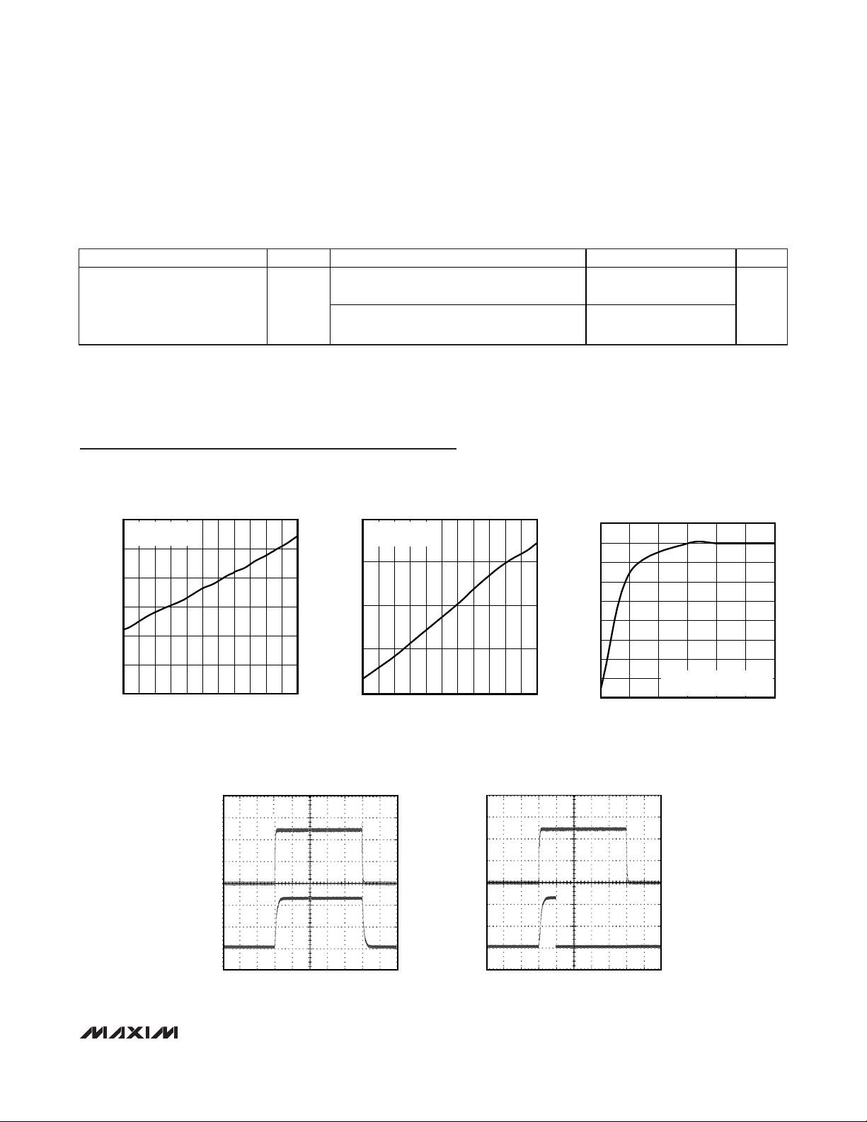
Typical Operating Characteristics
(V
CC
= +5V, unless otherwise noted.)
ELECTRICAL CHARACTERISTICS (continued)
(VCC= +2.5V to +5.5V, R
PULLUP
= 100kΩ (MAX6505/MAX6507 only), TA= -40°C to +125°C, unless otherwise noted. Typical values
are at T
A
= +25°C and VCC= +5V, unless otherwise noted.) (Note 1)
Note 1: 100% production tested at T
A
= +25°C. Specifications over temperature limits are guaranteed by design.
Note 2: T
ALARM
, T
UNDER
, and T
OVER
are factory-programmed temperature trip thresholds from -40°C to +125°C in 5°C increments.
Note 3: Temperature threshold hysteresis is defined as the difference from positive-going temperature thresholds minus the nega-
tive-going temperature thresholds.
PARAMETER SYMBOL CONDITIONS MIN TYP MAX UNITS
Open-Drain Output Leakage
Current
VCC = 5.5V, V
V
= 5.5V (MAX6505)
WARN
= 5.5V, VOK = 5.5V,
V
CC
= 5.5V (MAX6507)
V
OVER
ALARM
= 5.5V,
1
1
SUPPLY CURRENT
vs. TEMPERATURE
50
VCC = +5V
= 100kΩ
R
PULLUP
45
40
35
30
SUPPLY CURRENT (µA)
25
20
-40 -10 5 20-25 35 50 65 80 95 110 125
TEMPERATURE (°C)
MAX6505/8-01
HYSTERESIS vs. TRIP TEMPERATURE
2.5
VCC = +5V
= 100kΩ
R
PULLUP
2.0
1.5
HYSTERESIS (°C)
1.0
0.5
-40 -10 5-25 20 35 50 65 80 95 110 125
TEMPERATURE (°C)
0.1
MAX6505/8-02
0
-0.1
-0.2
-0.3
-0.4
-0.5
TRIP-POINT ERROR (%)
-0.6
-0.7
-0.8
TRIP-POINT ERROR (%)
vs. SUPPLY VOLTAGE
NORMALIZED TO TRIP-POINT
TEMPERATURE AT V
2.5 3.53.0 4.0 4.5 5.0 5.5
SUPPLY VOLTAGE (V)
CC
= +5V
μA
MAX6505/8-03
MAX6505
STARTUP DELAY
)
(T > T
TH
100µs/div
= 100kΩ
PULLUP
MAX6505/8-05
A
2V/div
B
A: V
B: ALARM VOLTAGE, R
MAX6505
STARTUP AND POWER-DOWN
)
(T < T
TH
100µs/div
PULSE
CC
PULLUP
= 100kΩ
MAX6505/8-04
A
2V/div
B
A: V
B: ALARM VOLTAGE, R
CC
PULSE
Page 4
MAX6505–MAX6508
Dual Trip SOT Temperature Switches
4 _______________________________________________________________________________________
Pin Description
PIN
MAX6505 MAX6506 MAX6507 MAX6508
1-—-—WARN
-— 1 -— -— WARN
2 2 2 2 GND Ground
3, 5 3, 5 -— -— S1, S0
-— -— 3 3 S0
4444V
-— -— 5 5 N.C. No Connection. Not internally connected.
-— -— 6 -—
-— -— _ 6 OVER
-— -— 1 -— OK
NAME FUNCTION
Open-Drain Active-Low Warning Output. WARN goes low
when the die temperature exceeds T
ΔT
AW.
Push-Pull Active-High Warning Output. WARN goes high
when the die temperature exceeds T
ΔT
AW.
Delta Temperature Select Input. Connect to V
select the difference between T
ALARM
1 or see Electrical Characteristics).
Hysteresis Select Input. Connect to V
hysteresis. Connect to GND for 2°C hysteresis.
CC
Supply Voltage Input. Bypass VCC to GND with a 0.1μF
ceramic capacitor.
Open-Drain Active-Low Overtemperature Output.
OVER
goes low when the die temperature exceeds the factoryset value of T
OVER
.
Push-Pull Active-High Overtemperature Output. OVER
goes high when the die temperature exceeds the factory-
set value of T
OVER.
Open-Drain Active-High Temperature Sensor Output. OK
goes high impedance when the die temperature is
between the factory-set values of T
When the die temperature is above T
T
, OK goes low.
UNDER
WARN
WARN
and T
CC
OVER
OVER
= T
ALARM
= T
ALARM
CC
WARN
for 10°C
and T
UNDER
or below
-
-
or GND to
(Table
OVER
.
Push-Pull Active-Low Temperature Sensor Output. OK
-— -— -—
1
OK
goes low when the die temperature is between the factoryset values of T
OVER
erature is above T
and T
OVER
or below T
. When the die temp-
UNDER
UNDER
Open-Drain Active-Low Alarm Output. ALARM goes low
6-—-—-—ALARM
when the die temperature exceeds the factory-set value of
.
T
ALARM
Push-Pull Active-High Alarm Output. ALARM goes high
-— 6 -— -— ALARM
when the die temperature exceeds the factory-set value of
.
T
ALARM
, OK goes high.
Page 5

MAX6505–MAX6508
Dual Trip SOT Temperature Switches
_______________________________________________________________________________________ 5
_______________Detailed Description
The MAX6505–MAX6508 fully integrated temperature
switches incorporate two temperature-dependent references and a comparator. One reference exhibits a positive temperature coefficient and the other a negative
temperature coefficient. The temperature at which the
two reference voltages are equal determines the temperature trip point. There are two versions, each of
which has two logic outputs.
The MAX6505/MAX6506 have a main trip point (T
ALARM
)
and a lower, “warning” trip point (T
WARN
). When the die
temperature rises above these trip points, the ALARM
and WARN outputs are asserted (Figure 1). The difference between the two trip points (ΔT
AW
) is pin selectable to +5°C, +10°C, +20°C, or +30°C by connecting
the two control pins (S0 and S1) high or low (Table 1).
MAX6505 has open-drain active-low outputs; MAX6506
has push-pull active-high outputs.
The MAX6507/MAX6508 have two factory-programmed
threshold temperatures (T
OVER
and T
UNDER
) and two
outputs (OK and OVER). One output (OK) asserts
when the temperature is between T
OVER
and T
UNDER
.
The other output (OVER) asserts when the temperature
is above T
OVER
. Table 4 shows the hex codes to determine the part numbers associated with specific values
of T
OVER
and T
UNDER
. The first hex code indicates the
lower trip point (T
UNDER
) and the second indicates the
higher trip point (T
OVER
). For example, a part with T
UN-
DER
= -10°C and T
OVER
= +75°C will have the part
number MAX6508UTA04B (Table 4 and Figure 2).
MAX6507 has open-drain outputs; MAX6508 has pushpull outputs.
Hysteresis Selection
The temperature threshold hysteresis for the ALARM
output of the MAX6505/MAX6506 is 2°C. The hysteresis
for the WARN output depends on the value of ΔTAW. If
ΔTAWis 5°C or 10°C (set by S0 and S1), WARN hys-
teresis is 5°C. If ΔTAWis 20°C or 30°C, WARN hysteresis is 10°C. MAX6507 and MAX6508 have pin-selectable
hysteresis of 2°C or 10°C for both OVER and OK outputs (Table 2).
Applications Information
Thermal Considerations
The MAX6505–MAX6508 supply current is typically
30µA. When used to drive high-impedance loads, the
devices dissipate negligible power. Therefore, the die
temperature is essentially the same as the package
temperature. The key to accurate temperature monitoring is good thermal contact between the MAX6505–
MAX6508 package and the device being monitored. In
some applications, the SOT23 packages may be small
enough to fit underneath a socketed microprocessor
(µP), allowing the device to monitor the µP’s temperature directly. Use the monitor’s output to reset the µP,
assert an interrupt, or trigger an external alarm.
Accurate temperature monitoring depends on the thermal resistance between the device being monitored
and the MAX6505–MAX6508 die.
The rise in die temperature due to self-heating is given
by the following formula:
ΔT
J
= P
DISSIPATION
✕
θ
JA
where P
DISSIPATION
is the power dissipated by the
MAX6505–MAX6508, and θJAis the package’s thermal
resistance. The typical thermal resistance is 115°C/W for
the SOT23 package. To limit the effects of self-heating,
minimize the output currents. For example, if the
MAX6505 sinks 5mA, the output voltage is guaranteed to
be less than 0.5V. Therefore, an additional 2.5mW of
Figure 1. Temperature Response—MAX6505UTP065 Outputs,
Δ
TAW= 10°C, and WARN Hysteresis ≈5°C
Table 1. MAX6505/MAX6506 ΔT
AW
Selection Table
CONTROL P INS DE SCR IPTION
T
S1 S0
GND GND 5
GND V
V
CC
V
CC
65°C
55°C
WARN
ALARM
CC
GND 20
V
CC
AW =TALARM
HYSTERESIS ≈ 2°C
HYSTERESIS ≈ 5°C
(°C)
10
30
– T
WARN
Page 6

MAX6505–MAX6508
Dual Trip SOT Temperature Switches
6 _______________________________________________________________________________________
Figure 2. Temperature Response—MAX6507A04B Outputs
with 2°C Hysteresis
Figure 3. Low-Power, High-Reliability, Fail-Safe Temperature
Monitor
Table 2. Hysteresis Selection
power is dissipated within the IC. This corresponds to a
+0.288°C shift in the die temperature in the SOT23.
Power Supply and Bypassing
The MAX6505 and MAX6508 operate from a singlesupply voltage in the +2.5V to +5.5V range. Connect a
0.1µF capacitor on the supply voltage line close to the
VCCpin for bypassing.
Low-Cost, Fail-Safe Temperature Monitor
The MAX6505/MAX6506 provide two outputs that can be
used for fail-safe temperature applications (Figure 3). For
example, the first output can activate a fan when the die
temperature exceeds a certain preset temperature. The
second output asserts at a higher temperature that could
be caused by a wide variety of destructive fault conditions, including latchup, short circuit, and cooling system
failure. This output can be used to initiate such actions
as shutdown of the entire system (see
Typical Operating
Circuits
)
.
The high-level integration, low cost, and small size of the
MAX6505–MAX6508 facilitate the use of multiple temperature monitors to increase system reliability.
PART
MAX6505
MAX6506
MAX6507
MAX6508
+75°C
TEMPERATURE
-10°C
OVER
OK
ALARM CONDITIONS WARN CONDITIONS OK, OVER
2°C—5°C ΔTWA = 5°C or 10°C
——10°C ΔT
-— — — — 2°C S0 = GND
-— — — — 10°C S0 = V
HYSTERESIS ≈ 2°C
-10°C
HYSFERESIS ≈ 2
TYPICAL THRESHOLD HYSTERESIS
= 20°C or 30°C
WA
°C
*
S1
S0
*ΔTAW = T
ALARM
- T
WARN
IS SET TO +30°C.
+2.5V TO +5.5V
V
CC
MAX6506
GND
ALARM
WARN
—
CC
SYSTEM
SHUTDOWN
FAN CONTROL
Page 7
MAX6505–MAX6508
Dual Trip SOT Temperature Switches
_______________________________________________________________________________________ 7
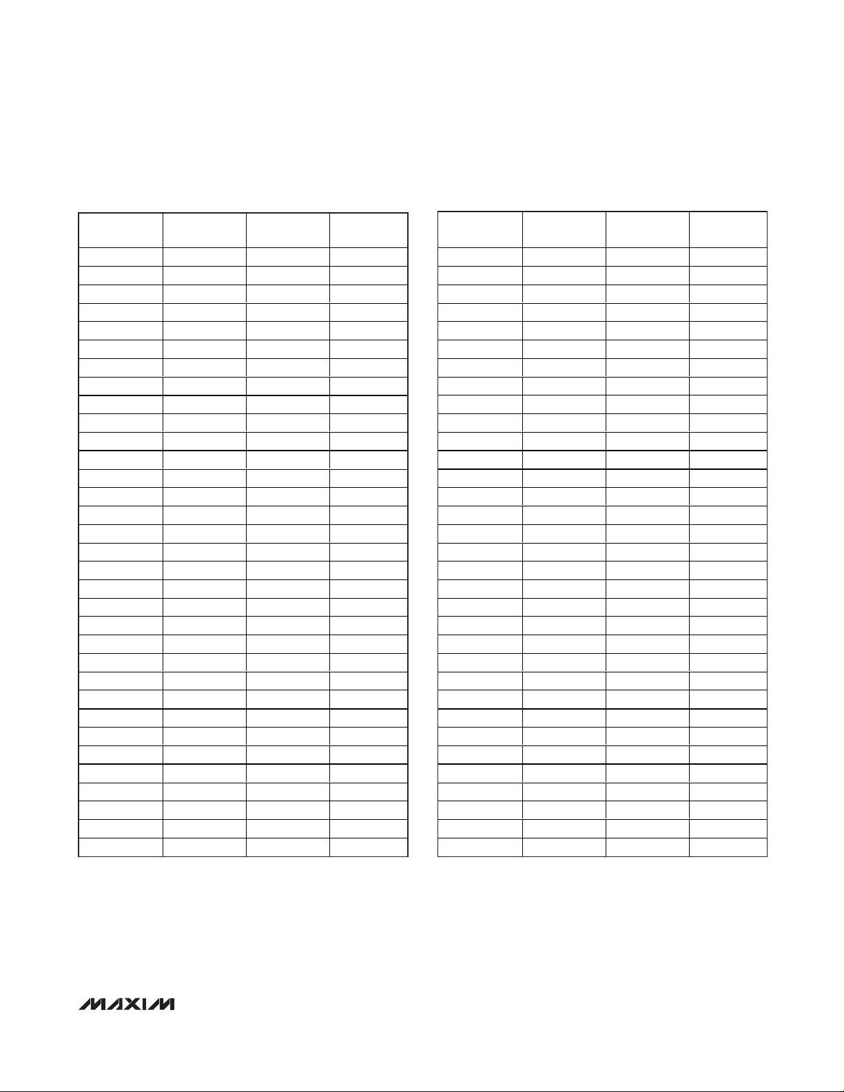
Table 3. MAX6505/MAX6506 Suffix and Top Mark Codes
PART SUFFIX
MAX6505 UTN035 -35 AAKK
MAX6505 UTN030 -30 AAKL
MAX6505 UTN025 -25 AAKM
MAX6505 UTN020 -20 AAKN
MAX6505 UTN015 -15 AAKO
MAX6505 UTN010 -10 AAKP
MAX6505 UTN005 -5 AAKQ
MAX6505 UTP000 0 AAKR
MAX6505 UTP005 5 AAKS
MAX6505 UTP010 10 AAKT
MAX6505 UTP015 15 AAKU
MAX6505 UTP020 20 AAKV
MAX6505 UTP025 25 AAKW
MAX6505 UTP030 30 AAKX
MAX6505 UTP035 35 AAKY
MAX6505 UTP040 40 AAKZ
MAX6505 UTP045 45 AALA
MAX6505 UTP050 50 AALB
MAX6505 UTP055 55 AALC
MAX6505 UTP060 60 AALD
MAX6505 UTP065 65 AALE
MAX6505 UTP070 70 AALF
MAX6505 UTP075 75 AALG
MAX6505 UTP080 80 AALH
MAX6505 UTP085 85 AALI
MAX6505 UTP090 90 AALJ
MAX6505 UTP095 95 AALK
MAX6505 UTP100 100 AALL
MAX6505 UTP105 105 AALM
MAX6505 UTP110 110 AALN
MAX6505 UTP115 115 AALO
MAX6505 UTP120 120 AALP
MAX6505 UTP125 125 AALQ
TRIP POINT
(°C)
TOP MARK
PART SUFFIX
MAX6506 UTN035 -35 AALR
MAX6506 UTN030 -30 AALS
MAX6506 UTN025 -25 AALT
MAX6506 UTN020 -20 AALU
MAX6506 UTN015 -15 AALV
MAX6506 UTN010 -10 AALW
MAX6506 UTN005 -5 AALX
MAX6506 UTP000 0 AALY
MAX6506 UTP005 5 AALZ
MAX6506 UTP010 10 AAMA
MAX6506 UTP015 15 AAMB
MAX6506 UTP020 20 AAMC
MAX6506 UTP025 25 AAMD
MAX6506 UTP030 30 AAME
MAX6506 UTP035 35 AAMF
MAX6506 UTP040 40 AAMG
MAX6506 UTP045 45 AAMH
MAX6506 UTP050 50 AAMI
MAX6506 UTP055 55 AAMJ
MAX6506 UTP060 60 AAMK
MAX6506 UTP065 65 AAML
MAX6506 UTP070 70 AAMM
MAX6506 UTP075 75 AAMN
MAX6506 UTP080 80 AAMO
MAX6506 UTP085 85 AAMP
MAX6506 UTP090 90 AAMQ
MAX6506 UTP095 95 AAMR
MAX6506 UTP100 100 AAMS
MAX6506 UTP105 105 AAMT
MAX6506 UTP110 110 AAMU
MAX6506 UTP115 115 AAMV
MAX6506 UTP120 120 AAMW
MAX6506 UTP125 125 AAMX
TRIP POINT
(°C)
TOP MARK
Page 8
Temperature-Window Alarm
The MAX6507 and MAX6508 have an output (OK, OK)
that indicates the die temperature is within the selected
temperature window. This output is asserted when
within the window, and deasserted when outside the
window. Additionally, a second digital output indicates
when the die temperature is above the upper set point.
This is useful in systems where operation is optimized
over a predetermined temperature range. The thermal
overrange signal can be used to assert a thermal shutdown, power-up, recalibration, or other temperaturedependent function (Figure 4 and
Typical Operating
Circuits
).
Chip Information
PROCESS: BiCMOS
MAX6505–MAX6508
Dual Trip SOT Temperature Switches
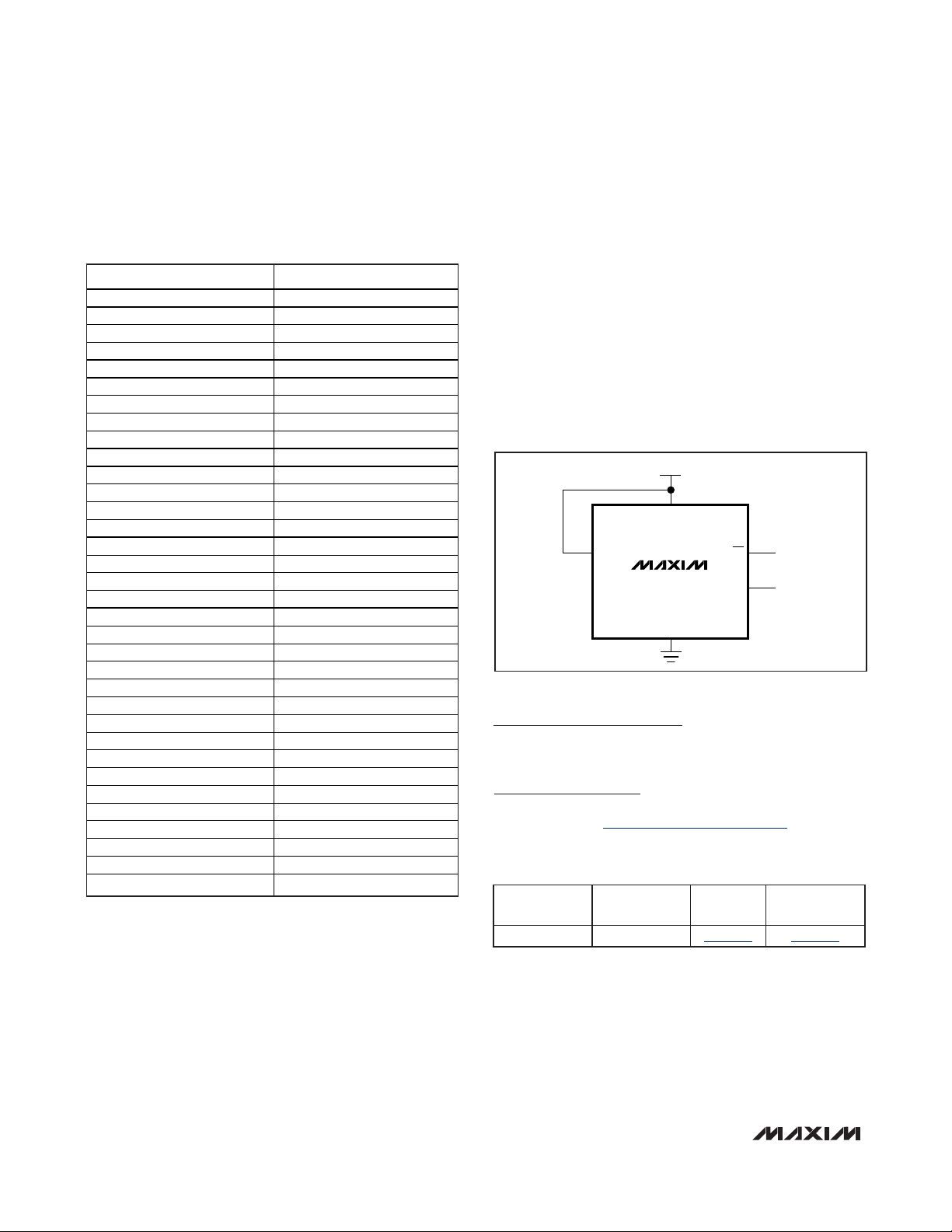
8 _______________________________________________________________________________________
Table 4. MAX6507/MAX6508 Trip
Temperature Code
*Two hex codes are used in the suffix. The first indicates the
the low trip temperature and the second indicates the high trip
temperature. For example, the MAX6507UT8255+T has a lower
trip point of -40
°
C and an upper trip point of +85°C.
Figure 4. Temperature-Window Alarms
Package Information
For the latest package outline information and land patterns
(footprints), go to www.maxim-ic.com/packages
. Note that a
“+”, “#”, or “-” in the package code indicates RoHS status only.
Package drawings may show a different suffix character, but
the drawing pertains to the package regardless of RoHS status.
PACKAGE
TYPE
PACKAGE
CODE
OUTLINE
NO.
LAND
PATTERN NO.
6 SOT23 U6SN+1
21-0058 90-0175
TRIP TEMPERATURE (°C) HEX CODE*
-40 82
-35 87
-30 8C
-25 91
-20 96
-15 9B
-10 A0
-5 A5
000
505
10 0A
15 0F
20 14
25 19
30 1E
35 23
40 28
45 2D
50 32
55 37
60 3C
65 41
70 46
75 4B
80 50
85 55
90 5A
95 5F
100 64
105 69
110 6E
115 73
120 78
125 7D
+2.5V TO +5.5V
V
CC
S0
MAX6508
GND
OK
OVER
OUT OF RANGE
SHUTDOWN
Page 9

MAX6505–MAX6508
+2.5V TO +5.5V
S1
S0
WARN
GND
FAN
V
CC
V
CC
ALARM
MAX6506
+2.5V TO +5.5V
S0
OVER
GND
V
CC
MAX6508
OK
+2.5V TO +5.5V
S1
S0
WARN
GND
V
CC
ALARM
MAX6505
INT
SHDN
R1R
2
GND
V
CC
μP
INT
GND
V
CC
μP
FAN
V
CC
INT
GND
V
CC
μP
Typical Operating Circuits
PART OUTPUT LOGIC OUTPUT STAGE
TEMPERATURE THRESHOLD
RANGE
MAX6505 ALARM, WARN Open Drain -40°C to +125°C
MAX6506 ALARM, WARN Push-Pull -40°C to +125°C
MAX6507 OVER, OK Open Drain -40°C to +125°C
MAX6508 OVER, OK Push-Pull -40°C to +125°C
Selector Guide
Dual Trip SOT Temperature Switches
_______________________________________________________________________________________ 9
Page 10

MAX6505–MAX6508
Dual Trip SOT Temperature Switches
Maxim cannot assume responsibility for use of any circuitry other than circuitry entirely embodied in a Maxim product. No circuit patent licenses are
implied. Maxim reserves the right to change the circuitry and specifications without notice at any time.
10
____________________Maxim Integrated Products, 120 San Gabriel Drive, Sunnyvale, CA 94086 408-737-7600
© 2011 Maxim Integrated Products Maxim is a registered trademark of Maxim Integrated Products, Inc.
Revision History
REVISION
NUMBER
0 4/00 Init ial release —
1 2/11
REVISION
DATE
DESCRIPTION
Changed all leaded parts to lead(Pb)-free parts in the Ordering Information table; in
the Absolute Maximum Ratings section changed the continuous power dissipation
numbers (7.1mW/°C to 8.7mW/°C and 571mW to 696mW) and added the sol dering
temperature; added the Package Information table
PAGES
CHANGED
1, 2, 8
 Loading...