

General Description
The MAX6469–MAX6484 are low-dropout linear regulators with a fully integrated microprocessor reset circuit.
Each is available with preset output voltages from +1.5V
to +3.3V in 100mV increments and delivers up to 300mA
of load current. These devices consume only 82µA of
supply current. The low supply current, low dropout voltage, and integrated reset functionality make these
devices ideal for battery-powered portable equipment.
The MAX6469–MAX6484 include a reset output that indicates when the regulator output drops below standard
microprocessor supply tolerances (-7.5% or -12.5% of
nominal output voltage). This eliminates the need for an
external microprocessor supervisor, while ensuring that
supply voltages and clock oscillators have stabilized
before processor activity is enabled. Push-pull and opendrain active-low reset outputs are available, with reset
timeout periods of 2.5ms, 20ms, 150ms, or 1200ms (min).
The MAX6469/MAX6470/MAX6473–MAX6478/MAX6481–
MAX6484 also have a shutdown feature that reduces the
supply current to 0.1µA (typ). The MAX6471–MAX6474/
MAX6479–MAX6482 offer a manual reset input to assert a
microprocessor reset while the regulator output is within
specification. The MAX6475/MAX6476/MAX6483/
MAX6484 feature a remote feedback sense pin for use
with an external NPN transistor for higher-current applications. The MAX6469–MAX6476 are available in 6-pin
SOT23 and 8-pin thin QFN packages. The MAX6477–
MAX6484 are available in a 3 × 3 chip-scale package
(UCSP™). All devices are specified for operation from
-40°C to +85°C.
Applications
Hand-Held Instruments (PDAs, Palmtops)
PCMCIA Cards/USB Devices
Cellular/Cordless Telephones
CD/DVD Drives
Notebook Computers
Digital Cameras
Bluetooth Modules/Wireless LAN
Features
♦ 3 ✕ 3 UCSP, 6-Pin SOT23, and 8-Pin QFN Packages
♦ Preset +1.5V to +3.3V Output (100mV Increments)
♦ SET Pin for Adjustable Output Voltage
♦ 75µV
RMS
LDO Output Voltage Noise
(MAX6477–MAX6484)
♦ ±2.0% Accuracy Over Temperature
♦ Guaranteed 300mA Output Current
♦ Low Dropout Voltage
55mV at 150mA
114mV at 300mA
♦ 82µA Supply Current, 0.1µA Shutdown Current
♦ Input Reverse Current, Thermal and Short-Circuit
Protection
♦ Microprocessor Reset with Four Timeout Options
♦ Push-Pull or Open-Drain RESET
♦ Manual Reset Input
♦ Remote Feedback Sense
MAX6469–MAX6484
300mA LDO Linear Regulators with
Internal Microprocessor Reset Circuit
________________________________________________________________ Maxim Integrated Products 1
Ordering Information
19-2532; Rev 2; 6/03
For pricing, delivery, and ordering information, please contact Maxim/Dallas Direct! at
1-888-629-4642, or visit Maxim’s website at www.maxim-ic.com.
Note: The first “_ _”are placeholders for the output voltage levels
of the devices. Desired output voltages are set by the suffix found
in the Output Voltage Suffix Guide (Table 1). The third “_” is a
placeholder for the reset threshold accuracy. Desired reset
threshold accuracy is set by the suffix found in the Reset
Threshold Accuracy Guide (Table 2). The “_” following the D is a
placeholder for the reset timeout delay time. Desired reset timeout
delay time is set by the suffix found in the Reset Timeout Delay
Guide (Table 3). For example, the MAX6481BL30BD4-T has a
3.0V output voltage, 12.5% reset threshold tolerance, and a
1200ms (min) reset timeout delay. Sample stock is generally available on standard versions only (Table 4). Standard versions
require a minimum order increment of 2.5k units. Nonstandard
versions must be ordered in 10k-unit increments. Contact factory
for availability.
Ordering Information continued at end of data sheet.
Pin Configurations appear at end of data sheet.
Typical Operating Circuits appear at end of data sheet.
UCSP is a trademark of Maxim Integrated Products, Inc.
*Future product—contact factory for availability.
EVALUATION KIT
AVAILABLE
MAX6469UT_ _ _D_-T -40°C to +85°C 6 SOT23-6
MAX6469TA_ _ _D_* -40°C to +85°C 8 Thin QFN
MAX6470UT_ _ _D_-T -40°C to +85°C 6 SOT23-6
MAX6470TA_ _ _D_* -40°C to +85°C 8 Thin QFN
PART TEMP RANGE
PINPACKAGE
MAX6469–MAX6484
300mA LDO Linear Regulators with Internal
Microprocessor Reset Circuit
2 _______________________________________________________________________________________
ABSOLUTE MAXIMUM RATINGS
(All voltages referenced to GND, unless otherwise noted.)
IN, SHDN, OUT, FB ..................................................-0.3V to +7V
MR, SET .......................................................-0.3V to (V
IN
+ 0.3V)
RESET (push-pull) ...................................-0.3V to (V
OUT
+ 0.3V)
RESET (open drain)..................................................-0.3V to +7V
OUT Short Circuit .......................................................Continuous
Input/Output Current (all pins except IN and OUT) ............20mA
Continuous Power Dissipation (T
A
= +70°C)
3 x 3 UCSP (derate 10.5mW/°C above +70°C) ............840mW
6-Pin SOT23 (derate 9.1mW/°C above +70°C).............727mW
8-Pin Thin QFN
(derate 24.4mW/°C above +70°C)..............................1951mW
Operating Temperature Range ..........................-40°C to +85°C
Junction Temperature......................................................+150°C
Storage Temperature Range .............................-65°C to +150°C
Lead Temperature (soldering, 10s) .................................+300°C
ELECTRICAL CHARACTERISTICS
(VIN= (V
OUT
+ 0.5V) or +2.5V, whichever is greater, C
OUT
= 3.3µF, TA= -40°C to +85°C. Typical specifications are at TA= +25°C,
unless otherwise noted.) (Note 2)
Dual Mode is a trademark of Maxim Integrated Products, Inc.
Stresses beyond those listed under “Absolute Maximum Ratings” may cause permanent damage to the device. These are stress ratings only, and functional
operation of the device at these or any other conditions beyond those indicated in the operational sections of the specifications is not implied. Exposure to
absolute maximum rating conditions for extended periods may affect device reliability.
Note 1: The MAX6477–MAX6484 are constructed using a unique set of packaging techniques that impose a limit on the thermal pro-
file the devices can be exposed to during board-level solder attach and rework. This limit permits only the use of the solder
profiles recommended in the industry-standard specification, JEDEC 020A, paragraph 7.6, Table 3 for IR/VPR and
Convection reflow. Pre-heating is required. Hand or wave soldering is not allowed.
Input Voltage Range V
Input Undervoltage Lockout V
Supply Current (Ground Current) I
Shutdown Supply Current I
REGULATOR CIRCUIT
Output Current 300 mA
Output Voltage Accuracy (Fixed
Output Voltage Operation,
Table 1) MAX6469–MAX6476
Output Voltage Accuracy (Fixed
Output Voltage Operation,
Table 1) MAX6477–MAX6484
Adjustable Output Voltage Range V
SET Reference Voltage V
SET Dual ModeTM Threshold 185 mV
SET Input Leakage Current I
PARAMETER SYMBOL CONDITIONS MIN TYP MAX UNITS
IN
UVLO
Q
SHDN
SET
SET
VIN falling 2.25 2.47 V
I
= 0 82 136
OUT
I
= 300mA 96
OUT
TA = +25°C 0.1 1 µA
1mA ≤ I
OUT
1mA ≤ I
OUT
1mA ≤ I
OUT
2mA ≤ I
OUT
2mA ≤ I
OUT
2mA ≤ I
OUT
(Note 3)
V
= 0, +1.2V (Note 3) ±20 ±100 nA
SET
≤ 150mA, TA = +25°C -1.3 +1.3
≤ 150mA, TA = -40°C to +85°C -2.3 +2.3
≤ 300mA, TA = -40°C to +85°C -2.7 +2.7
≤ 100mA, TA = +25°C -1.1 +1.1
≤ 100mA, TA = -40°C to +85°C -2.0 +2.0
≤ 300mA, TA = -40°C to +85°C
2.5 5.5 V
-2.5 +2.5
SET
1.200 1.229 1.258 V
5.0 V
µA
%
%
MAX6469–MAX6484
300mA LDO Linear Regulators with Internal
Microprocessor Reset Circuit
_______________________________________________________________________________________ 3
ELECTRICAL CHARACTERISTICS (continued)
(VIN= (V
OUT
+ 0.5V) or +2.5V, whichever is greater, C
OUT
= 3.3µF, TA= -40°C to +85°C. Typical specifications are at TA= +25°C,
unless otherwise noted.) (Note 2)
Dropout Voltage
(Notes 3, 4)
Output Current Limit VIN ≥ 2.5V (Note 3) 450 mA
Input Reverse Leakage Current
(OUT to IN Leakage Current)
Startup Time Response
SHDN Input Low Voltage V
SHDN Input High Voltage V
SHDN Input Current SHDN = VIN or GND -1 0.1 +1 µA
Thermal-Shutdown Temperature T
Thermal-Shutdown Hysteresis ∆T
Line Regulation
Load Regulation
Output Voltage Noise
RESET CIRCUIT
V
OUT
(V
FB
MAX6483/MAX6484) (Note 5)
V
OUT
(V
FB
MAX6483/MAX6484)
Reset Timeout Period
(Note 6)
PARAMETER SYMBOL CONDITIONS MIN TYP MAX UNITS
I
= 50mA 23 32
OUT
I
= 150mA 55 90
OUT
I
= 300mA 114 180
OUT
I
= 50mA 25 40
OUT
I
= 150mA 61 100
OUT
I
= 300mA 114 190
OUT
I
= 50mA 26 50
OUT
I
= 150mA 65 110
OUT
I
= 300mA 137 210
OUT
I
= 50mA 30 60
OUT
I
= 150mA 75 150
OUT
I
= 300mA 158 250
OUT
OUT
20 µs
0.7 × V
IN
180 °C
20 °C
0.09 %/V
≤
OUT
0.2 %
MAX6469–MAX6476 150
MAX6477–MAX6484 75
0.3 × V
Reset Threshold
for MAX6475/MAX6476/
∆V
SHDN
SHDN
V
THOUT
V
= +3.3V
OUT
(fixed output operation)
V
= +3.0V
OUT
(fixed output operation)
DO
V
= +2.8V
OUT
(fixed output operation)
V
= +2.5V
OUT
(fixed output operation)
= 4V, V
V
IN
Rising edge of V
= 5.5V, SHDN deasserted 0.01 1.5 µA
OUT
or SHDN to V
IN
within specification, RL = 68Ω, SET = GND,
= 10mA
I
OUT
IL
IH
V
= 1.5V, 2.5V ≤ VIN ≤ 5.5V,
OUT
= 10mA
I
OUT
V
= 1.5V, VIN = 2.5V, 1mA ≤ I
OUT
150mA
10Hz to 100kHz,
C
= 0.1µF,
IN
= 100mA,
I
OUT
V
= 1.5V
OUT
MAX64_ _ _ _ _ _ A 90 92.5 95
MAX64_ _ _ _ _ _ B 85 87.5 90
to Reset Delay
for MAX6475/MAX6476/
35 µs
D1 2.5 3.75 5.0
t
RP
D2 20 30 40
D3 150 225 300
D4 1200 1800 2400
IN
µV
%V
mV
V
V
RMS
OUT
ms
MAX6469–MAX6484
300mA LDO Linear Regulators with Internal
Microprocessor Reset Circuit
4 _______________________________________________________________________________________
Note 2: All devices are 100% production tested at +25°C and are guaranteed by correlation for TA= T
MIN
to T
MAX
.
Note 3: Guaranteed by design.
Note 4: Dropout voltage is defined as (V
IN
- V
OUT
) when V
OUT
is 2% below the value of V
OUT
for VIN= V
OUT(NOM)
+ 1V.
Note 5: MAX6473/MAX6474/MAX6481/MAX6482 are guaranteed by design for V
OUT
< 2.5V.
Note 6: Select the reset timeout period using the Reset Timeout Delay Guide (Table 3). Insert the appropriate suffix in the part number
when ordering.
ELECTRICAL CHARACTERISTICS (continued)
(VIN= (V
OUT
+ 0.5V) or +2.5V, whichever is greater, C
OUT
= 3.3µF, TA= -40°C to +85°C. Typical specifications are at TA= +25°C,
unless otherwise noted.) (Note 2)
Typical Operating Characteristics
(VIN= 5V, V
OUT
= 3.3V, C
OUT
= 3.3µF, TA= +25°C, unless otherwise noted.)
MR Input Low Voltage V
MR Input High Voltage V
MR Minimum Input Pulse 1µs
MR Glitch Rejection 120 ns
MR to Reset Delay 200 ns
MR Pullup Resistance MR to OUT 25 40 70 kΩ
RESET Output Voltage
(Open Drain)
Open-Drain Reset Output
Leakage Current
RESET Output Voltage Push-Pull
PARAMETER SYMBOL CONDITIONS MIN TYP MAX UNITS
0.3 ×
V
OUT
1µA
V
I
LKG
V
V
IL
IH
OL
OL
OH
(Note 3)
V
≥ 1.0V, I
OUT
V
≥ 1.5V , I
OU T
(Note 3)
V
≥ 1.0V, I
OUT
V
≥ 1.5V , I
OU T
V
≥ 2.0V, I
OUT
deasserted
0.7 ×
V
OUT
= 50µA, RESET asserted 0.3
SINK
= 3.2m A, RES ET asser ted 0.4
S IN K
= 50µA, RESET asserted 0.3
SINK
= 3.2m A, RES ET asser ted 0.4
S IN K
SOURCE
= 500µA, RESET
0.8 ×
V
OUT
V
V
V
V
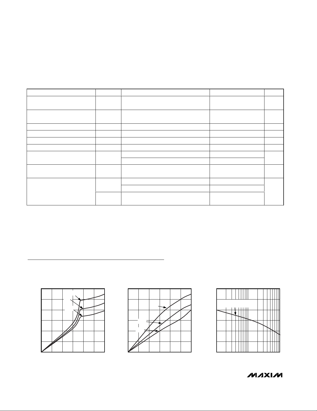
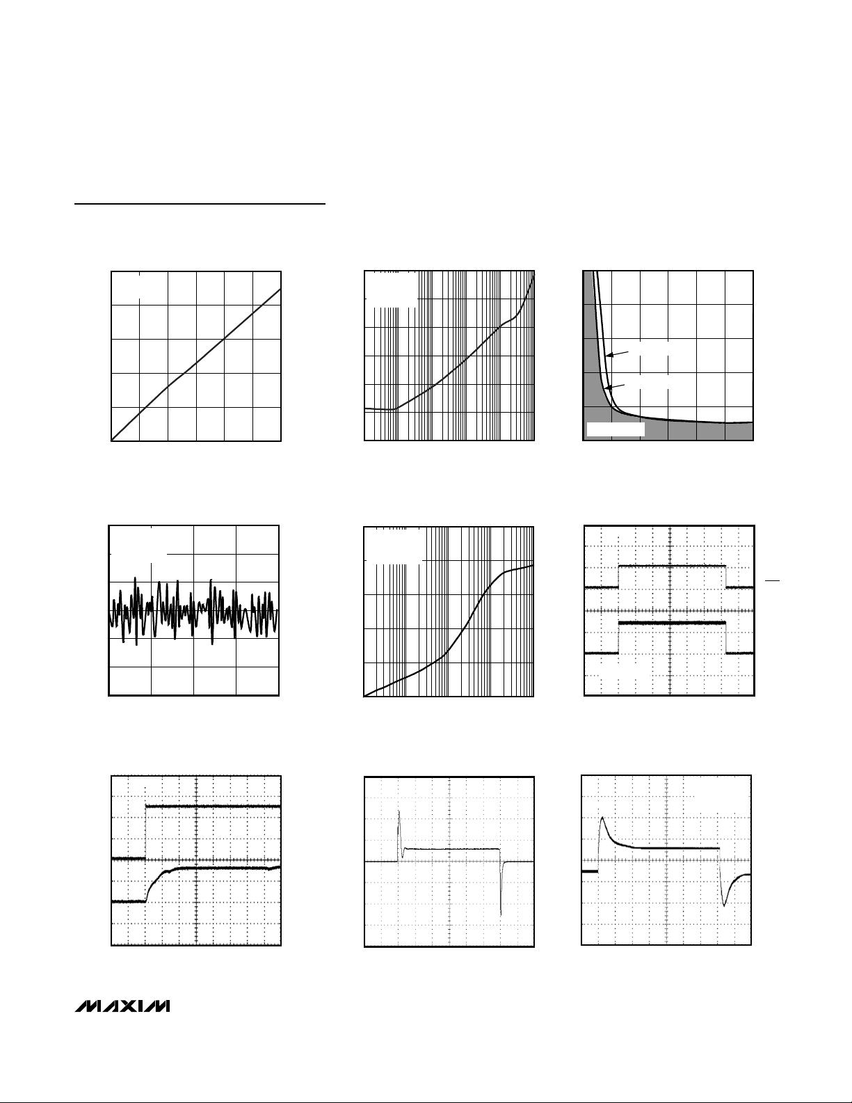
GROUND CURRENT vs. INPUT VOLTAGE
120
100
80
60
40
GROUND CURRENT (µA)
20
0
06
INPUT VOLTAGE (V)
(NO LOAD)
+85°C
+25°C
-40°C
GROUND CURRENT vs. INPUT VOLTAGE
(300mA LOAD)
120
100
MAX6469 toc01
80
60
40
GROUND CURRENT (µA)
20
54321
0
+85°C
+25°C
-40°C
INPUT VOLTAGE (V)
MAXIMUM TRANSIENT DURATION
vs. RESET THRESHOLD OVERDRIVE
150
125
MAX6469 toc02
PULSE DURATION (µs)
5432106
RESET ASSERTS ABOVE
THIS LINE
100
75
50
25
0
1 100
RESET THRESHOLD OVERDRIVE (mV)
10
MAX6469 toc03
MAX6469–MAX6484
300mA LDO Linear Regulators with Internal
Microprocessor Reset Circuit
_______________________________________________________________________________________ 5
Typical Operating Characteristics (continued)
(VIN= 5V, V
OUT
= 3.3V, C
OUT
= 3.3µF, TA= +25°C, unless otherwise noted.)
DROPOUT VOLTAGE vs. LOAD CURRENT
125
V
= 3.3V
OUT
= 3.3µF
C
OUT
100
75
50
DROPOUT VOLTAGE (mV)
25
0
0 300
LOAD CURRENT (mA)
OUTPUT NOISE
VIN = 4.5V
= 3.3V
V
OUT
= 100mA
I
LOAD
PSRR vs. FREQUENCY
V
= 3.3V
OUT
= 3.3µF
C
OUT
= 30mA
I
LOAD
OUTPUT NOISE vs. FREQUENCY
VIN = 2.5V
= 1.5V
V
OUT
= 100mA
I
OUT
25020015010050
MAX6469 toc07
MAX6469 toc04
100µV/div
0
-10
-20
-30
PSRR (dB)
-40
-50
-60
0.01 1000
100
80
60
(µV)
RMS
V
40
20
FREQUENCY (kHz)
REGION OF STABLE C
vs. LOAD CURRENT
5
MAX6469 toc05
4
3
ESR (Ω)
OUT
2
C
1
0
1001010.1
0300
C
C
OUT
STABLE REGION
LOAD CURRENT (mA)
OUT
= 4.7µF
= 3.3µF
SHUTDOWN RESPONSE
MAX6469 toc08
I
= 50mA
LOAD
OUT
ESR
25020015010050
MAX6469 toc09
MAX6469 toc06
V
SHDN
5V/div
V
OUT
2V/div
500µs/div
0
10 100 10k 100k
1k
FREQUENCY (Hz)
20ms/div
LOAD-TRANSIENT RESPONSE
STARTUP RESPONSE
10µs/div
MAX6469 toc10
V
IN
2V/div
V
OUT
2V/div
LOAD-TRANSIENT RESPONSE
100µs/div
MAX6469 toc11
V
OUT
20mV/div
NEAR DROPOUT
10µs/div
V
IN
V
OUT
I
LOAD
MAX6469 toc12
= 5V
= 3.3V
= 100mA
V
OUT
5mV/div

MAX6469–MAX6484
300mA LDO Linear Regulators with Internal
Microprocessor Reset Circuit
6 _______________________________________________________________________________________
Typical Operating Characteristics (continued)
(VIN= 5V, V
OUT
= 3.3V, C
OUT
= 3.3µF, TA= +25°C, unless otherwise noted.)
V
OUT
I
LOAD
LINE TRANSIENT RESPONSE
= 3.3V
= 10mA
100µs/div
MAX6469 toc13
5V
V
IN
500mV/div
4.5V
V
OUT
20mV/div
AC-COUPLED
RESET DELAY RESPONSE
200ms/div
MAX6469 toc14
V
IN
1V TO 4V
2V/div
RESET
2V/div
RESET RESPONSE TO MR
200ns/div
MAX6469 toc15
MR
2V/div
RESET
2V/div
RESET RESPONSE TO VIN RISING
200ms/div
MAX6469 toc16
RESET
2V/div
V
OUT
2V/div
V
IN
5V/div
NORMALIZED OUTPUT VOLTAGE
vs. TEMPERATURE
1.012
NORMALIZED TO +25°C
1.006
I
= 10mA
LOAD
1.000
I
= 300mA
I
= 150mA
LOAD
0.994
NORMALIZED OUTPUT VOLTAGE
0.988
-40 85
LOAD
TEMPERATURE (°C)
MAX6469 toc17
603510-15

MAX6469–MAX6484
300mA LDO Linear Regulators with Internal
Microprocessor Reset Circuit
_______________________________________________________________________________________ 7
MAX6469/MAX6470/MAX6477/MAX6478 Pin Description
MAX6471/MAX6472/MAX6479/MAX6480 Pin Description
PIN BUMP
MAX6469/MAX6470 MAX6477/MAX6478
SOT23 QFN UCSP
1 1, 2 A1 IN Regulator Input. Bypass IN to GND with a 0.1µF capacitor.
2 3 A2 GND
34 A3 SHDN
45 C3 RESET
5 6 C2 SET
6 7, 8 C1 OUT
NAME FUNCTION
Ground. This pin also functions as a heatsink. Solder to large pads or
the circuit-board ground plane to maximize thermal dissipation.
Active-Low Shutdown Input. Connect SHDN to V
operation.
Active-Low Reset Output. RESET remains low while V
reset threshold. RESET remains low for the duration of the reset timeout
period after the reset conditions are terminated. RESET is available in
open-drain and push-pull configurations.
Feedback Input for Externally Setting the Output Voltage. Connect SET
to GND to select the preset output voltage. Connect SET to an external
resistor-divider network for adjustable output operation.
Regulator Output. Bypass OUT to GND with a minimum 3.3µF low-ESR
capacitor.
IN
PIN BUMP
MAX6471/MAX6472 MAX6479/MAX6480
SOT23 QFN UCSP
1 1, 2 A1 IN Regulator Input. Bypass IN to GND with a 0.1µF capacitor.
2 3 A2 GND
34 A3 MR
45 C3 RESET
NAME FUNCTION
Ground. This pin also functions as a heatsink. Solder to large pads or
the circuit-board ground plane to maximize thermal dissipation.
Active-Low Manual Reset Input. The reset output is asserted while MR
is pulled low and remains asserted for the duration of the reset timeout
period after MR transitions from low to high. Leave MR unconnected or
connect to V
(typ) to V
Active-Low Reset Output. RESET remains low while V
reset threshold or while MR is held low. RESET remains low for the
duration of the reset timeout period after the reset conditions are
terminated. RESET is available in open-drain and push-pull
configurations.
if not used. MR has an internal pullup resistor of 40kΩ
OUT
.
OUT
for normal
is below the
OUT
is below the
OUT
5 6 C2 SET
6 7, 8 C1 OUT
Feedback Input for Externally Setting the Output Voltage. Connect SET
to GND to select the preset output voltage. Connect SET to an external
resistor-divider network for adjustable output operation.
Regulator Output. Bypass OUT to GND with a minimum 3.3µF low-ESR
capacitor.

MAX6469–MAX6484
300mA LDO Linear Regulators with Internal
Microprocessor Reset Circuit
8 _______________________________________________________________________________________
MAX6473/MAX6474/MAX6481/MAX6482 Pin Description
MAX6475/MAX6476/MAX6483/MAX6484 Pin Description
PIN BUMP
MAX6473/MAX6474 MAX6481/MAX6482
SOT23 QFN UCSP
1 1, 2 A1 IN Regulator Input. Bypass IN to GND with a 0.1µF capacitor.
2 3 A2 GND
34 A3 SHDN
45 C3 RESET
56 C2 MR
6 7, 8 C1 OUT
NAME FUNCTION
Ground. This pin also functions as a heatsink. Solder to large pads or
the circuit-board ground plane to maximize thermal dissipation.
Active-Low Shutdown Input. Connect SHDN to V
operation.
Active-Low Reset Output. RESET remains low while V
reset threshold or while MR is held low. RESET remains low for the
duration of the reset timeout period after the reset conditions are
terminated. RESET is available in open-drain and push-pull
configurations.
Active-Low Manual Reset Input. The reset output is asserted while MR
is pulled low and remains asserted for the duration of the reset timeout
period after MR transitions from low to high. Leave MR unconnected or
connect to V
(typ) to V
Regulator Output. Bypass OUT to GND with a minimum 3.3µF (min)
low-ESR capacitor.
if not used. MR has an internal pullup resistor of 40kΩ
OUT
.
OUT
for normal
IN
OUT
is below the
PIN BUMP
MAX6475/MAX6476 MAX6483/MAX6484
SOT23 QFN UCSP
1 1, 2 A1 IN Regulator Input. Bypass IN to GND with a 0.1µF capacitor.
2 3 A2 GND
34 A3 SHDN
45 C3 RESET
5 6 C2 FB
6 7, 8 C1 OUT
NAME FUNCTION
Ground. This pin also functions as a heatsink. Solder to large pads or
the circuit-board ground plane to maximize thermal dissipation.
Active-Low Shutdown Input. Connect SHDN to V
operation.
Active-Low Reset Output. RESET remains low while FB is below the
reset threshold. RESET remains low for the duration of the reset
timeout period after the reset conditions are terminated. RESET is
available in open-drain and push-pull configurations.
Feedback Input for Linear Regulator Controller or Remote Sense
Applications. Connect FB to the external load (VCC) to obtain the fixed
output voltage.
Regulator Output. Bypass OUT to GND with a minimum 3.3µF low-ESR
capacitor.
IN
for normal

MAX6469–MAX6484
300mA LDO Linear Regulators with Internal
Microprocessor Reset Circuit
_______________________________________________________________________________________ 9
Detailed Description
The MAX6469–MAX6484 are ultra-low, quiescent current, low-dropout linear regulators with an integrated
microprocessor reset circuit. These devices guarantee
300mA (min) drive capabilities and are available with
preset output voltages in 100mV increments between
+1.5V and +3.3V. The internal reset circuit monitors the
regulator output voltage and asserts the reset output
when the regulator output is below the microprocessor
supply tolerance.
Regulator
The regulator core operates with +2.5V to +5.5V input
voltage range. The output voltage is offered in 100mV
increments between +1.5V and +3.3V (contact factory
for other output voltage options). The MAX6469–
MAX6472/MAX6477–MAX6480 offer an adjustable output voltage implemented with an external resistordivider network between OUT, SET, and GND (Figure
1). SET must be connected to either GND for fixed
V
OUT
or to an external divider for adjustable V
OUT
. The
MAX6469–MAX6472/MAX6477–MAX6480 automatically
determine the feedback path depending on the connection of SET. The Typical Operating Circuit shows a
typical connection for the MAX6469. OUT is an internally regulated low-dropout (LDO) linear regulator that
powers a microprocessor.
Reset Circuit
The reset supervisor circuit is fully integrated in the
MAX6469–MAX6484 and uses the same reference voltage as the regulator. Two supply tolerance reset
thresholds, -7.5% and -12.5%, are provided for each
type of device.
-7.5% Reset: Reset does not assert until the regulator
output voltage is at least -5% out of tolerance and
always asserts before the regulator output voltage is
-10% out of tolerance.
-12.5% Reset: Reset does not assert until the regulator
output voltage is at least -10% out of tolerance and
always asserts before the regulator output voltage is
-15% out of tolerance.
RESET
Output
A µP’s reset input starts the µP in a known state. The
MAX6469–MAX6484 µP supervisory circuits assert
RESET during power-up, power-down, and brownout
conditions. RESET asserts when the input voltage is
below the undervoltage lockout threshold. RESET
asserts when V
OUT
is below the reset threshold and
remains asserted for at least the minimum selected reset
timeout period (tRP, Table 3) after VINrises above the
undervoltage lockout threshold and V
OUT
rises above
the reset threshold. RESET asserts when MR is pulled
low (MAX6471–MAX6474/MAX6479–MAX6482). RESET
asserts when SHDN is pulled low (MAX6469/
MAX6470/MAX6473–MAX6478/MAX6481–MAX6484).
Shutdown
(MAX6469/MAX6470/MAX6473–MAX6478/MAX6481–
MAX6484 only)
SHDN allows the regulator to shut down, thereby reducing the total I
IN
consumption of the device. SHDN pro-
vides a digitally controlled active-low shutdown. In
shutdown mode, the pass transistor, control circuit, and
reference turn off to reduce the supply current to below
0.1µA. Connect SHDN to IN for normal operation.
Manual Reset Input
(MAX6471–MAX6474/MAX6479–MAX6482 only)
Many µP-based products require manual reset capability, allowing the operator, a test technician, or external
logic circuitry to initiate a reset. A logic low on MR
asserts reset while the regulator output voltage is still
within tolerance.
Reset remains asserted while MR is low and for the
reset timeout period (tRP) after MR returns high. The
MR input has an internal pullup of 40kΩ (typ) to OUT.
MR can be driven with TTL/CMOS logic levels or with
open-drain/collector outputs. Connect a normally open
switch from MR to GND to create a manual reset function; external debounce circuitry is not required. If MR
is driven from long cables or the device is used in a
noisy environment, connect a 0.1µF capacitor from MR
to GND to provide additional noise immunity.
Feedback Input
(MAX6475/MAX6476/MAX6483/MAX6484 only)
The feedback input (FB) connects to an internal resistordivider network (Functional Diagram). FB is not internally
connected to V
OUT
, and as a result can be used to
Figure 1. Adjustable Output Voltage Configuration
2.5V TO 5.5V
IN
OUT
MAX6469–MAX6472
MAX6477–MAX6480
MANUAL
RESET
( ) ARE FOR MAX6471/MAX6472/MAX6479/MAX6480 ONLY
(MR)
SET
GND
R1
C
OUT
R2

MAX6469–MAX6484
300mA LDO Linear Regulators with Internal
Microprocessor Reset Circuit
10 ______________________________________________________________________________________
remotely sense the output voltage of the device. Using
FB with an external NPN transistor, the current drive
capability can be increased according to the following
equation (Figure 2):
I
OUT(TOTAL)
= I
OUT
✕ (β+1)
The external NPN pass transistor must meet specifications for current gain, power dissipation, and collector
current. The beta influences the maximum output current the circuit can deliver. The largest guaranteed output current is given by I
LOAD
(max) = 300mA × beta
(min). The transistor’s rated power dissipation must
exceed the actual power dissipated in the transistor.
The power dissipated (PD) equals the maximum load
current (I
LOAD
(max)) times the maximum input-to-out-
put voltage differential: PD = I
LOAD
(max) × (V
IN
(max) -
V
OUT
). The rated transistor collector current must
exceed the maximum load current.
Reverse Leakage Protection
Reverse OUT to IN Current
An internal circuit monitors the MAX6469–MAX6484
input and output voltages. When the output voltage is
greater than the input voltage, the internal IN-to-OUT
pass transistor and parasitic diode turn off. An external
voltage applied to OUT does not reverse charge a battery or power source applied to IN (the leakage path
from OUT to IN is 0.01µA typ). When the output voltage
exceeds the input voltage, OUT powers the device and
shutdown must be logic high (greater than 0.7
✕
V
OUT
).
RESET asserts until IN exceeds OUT and OUT is above
the specified V
THOUT
threshold (based on the selected
or adjusted regulator OUT nominal voltage).
Reverse OUT to Ground Current
The MAX6469–MAX6484 maintain a low OUT-to-GND
reverse-current flow when the IN power source is
removed. When IN floats (input battery removed) and
SHDN is pulled up to V
OUT
(by an external diode), the
OUT-to-GND current through the LDO is 40µA (typ). The
regulator output can be held up with an external super
capacitor or backup battery at OUT until the IN battery is
replaced. The RESET output is asserted while the IN battery is removed to place the system in a low-power
mode. Volatile memory content is maintained until the
super capacitor or battery voltage drops below RAM
standby specifications. RESET deasserts when the IN
battery has been replaced and OUT exceeds the
desired reset threshold. For nonrechargeable backup
battery applications, place a reverse diode between
OUT and the backup battery (to prevent battery charging). The external diode does not affect the regulator’s
dropout voltage because it is not between the LDO output and the processor/memory Vcc supply. The diode
can be replaced with a current-limiting resistor for
rechargeable backup battery applications.
Current Limit
The MAX6469–MAX6484 include an internal currentlimit circuit that monitors and controls the pass transistor’s gate voltage, limiting the output current to 450mA
(min). The output can be shorted to ground indefinitely
without damaging the part.
Thermal Shutdown
When the junction temperature (TJ) exceeds +180°C
(typ), the thermal sensor signals the shutdown logic,
turning off the pass transistor and allowing the IC to
Figure 3. Battery Backup
Figure 2. High-Current, External Transistor Application
5.0V
IN
OUT
MAX6475/MAX6476
MAX6483/MAX6484
GND
FB
RESET
R
0.1µF3.3µF330Ω
PULLUP
VCC = 3.3V1A TOTAL CURRENT
µP
REMOVABLE
LITHIUM ION OR
3-CELL
ALKALINE
REMOVABLE
LITHIUM ION OR
3-CELL
ALKALINE
MAX6469–
MAX6484
SHDN
IN
MAX6469–
MAX6484
SHDN
OUTIN
OUT
3.3µF
3.0V
LITHIUM
3.3µF
SUPERCAP
µP MEMORY
µP MEMORY

MAX6469–MAX6484
300mA LDO Linear Regulators with Internal
Microprocessor Reset Circuit
______________________________________________________________________________________ 11
cool. The thermal sensor turns the pass transistor on
again after the IC’s junction temperature cools by 20°C,
resulting in a pulsed output during continuous thermal
overload conditions. Thermal overload protection is
designed to protect the MAX6469–MAX6484 in the
event of fault conditions. For continuous operation, do
not exceed the absolute maximum junction temperature
rating of T
JMAX
= +150°C.
Operating Region and Power Dissipation
The MAX6469–MAX6484’s maximum power dissipation
depends on the thermal resistance of the case and circuit board, the temperature difference between the die
junction and the ambient air, and the rate of airflow. The
power dissipation across the device is:
P = I
OUT(VIN
- V
OUT
)
The maximum power dissipation is:
P
MAX
= (TJ- TA) / (ØJB+ ØBA)
where TJ- TAis the temperature difference between the
die junction and the surrounding air, ØJB(or ØJC) is the
thermal resistance of the package, and ØBAis the thermal resistance through the PC board, copper traces,
and other materials to the surrounding air. The
MAX6469–MAX6476 QFN package ØJC= 41°C/W, and
the MAX6469–MAX6476 SOT package ØJC= 110°C/W.
The MAX6469–MAX6484’s ground pin (GND) performs
the dual function of providing an electrical connection
to the system ground and channeling heat away.
Connect GND to the system ground using a large pad
or ground plane. For continuous operation, do not
exceed the absolute maximum junction temperature
rating of T
JMAX
= +150°C.
Applications Information
Output Voltage Selection
The MAX6469–MAX6484 feature dual-mode operation:
they operate in either a preset output voltage mode
or an adjustable mode. In preset voltage mode, internal
feedback resistors set the MAX6469–MAX6484’s output
from +1.5V to +3.3V (Table 1). Select this mode by connecting SET to ground (MAX6469–MAX6472/
MAX6477–MAX6480). In adjustable mode, select an
output between 1.25V and 5.5V using two external
resistors connected as a voltage-divider to SET (Figure
1). The output voltage is set by the following equation:
V
OUT
= V
SET
(1 + R1 / R2)
where V
SET
= 1.23V. To simplify resistor selection:
R1 = R2(V
OUT
/ V
SET
- 1)
Choose R2 = 50kΩ to maintain stability, accuracy and
high-frequency power-supply rejection. Avoid selecting
resistor values greater than 100kΩ. In preset voltage
mode, the impedance between SET and ground should
always be less than 50kΩ. In most applications, connect SET directly to ground.
Low-Noise UCSP Output
MAX6477–MAX6484 UCSP products include internal filtering to yield low output noise without an additional
external bypass capacitor. The devices yield 75µV
RMS
(typ) output noise (for V
OUT
= 3.0V) and 150µV
RMS
(for
V
OUT
= 3.3V). This low-noise feature makes the
MAX6477–MAX6484 ideal for audio applications.
Capacitor Selection and Regulator
Stability
For stable operation over the full temperature range
and with load currents up to 300mA, use a 3.3µF (min)
ceramic output capacitor with an ESR <0.2Ω. To
reduce noise and improve load transient response, stability, and power-supply rejection, use large output
capacitor values such as 10µF.
Note that some ceramic capacitors exhibit large capacitance and ESR variation with temperature. With capacitor dielectrics such as Z5U and Y5V, use 4.7µF or more
to ensure stability over temperature. With X7R or X5R
capacitor dielectrics, 3.3µF should be sufficient at all
operating temperatures. Higher ESR capacitors require
more capacitance to maintain stability. A graph of the
Region of Stable ESR vs. Load Current is shown in the
Typical Operating Characteristics.
To improve power-supply rejection and transient
response, use a 1µF capacitor between IN and GND.
The MAX6469–MAX6484 remain stable with purely
resistive loads or current loads up to 300mA.
Reset Transient Immunity
The reset circuit is relatively immune to short-duration,
falling V
OUT
transients. The Typical Operating
Characteristics section shows a graph of the Maximum
Transient Duration vs. Reset Threshold Overdrive for
which reset is not asserted. The graph was produced
using falling V
OUT
transients starting at V
OUT
and ending below the reset threshold by the magnitude indicated (reset threshold overdrive). The graph shows the
maximum pulse width that a falling V
OUT
transient can
typically have without triggering a reset pulse. As the
amplitude of the transient increases (i.e., goes further
below the reset threshold), the maximum allowable
pulse width decreases. Typically, a V
OUT
transient that
goes only 10mV below the reset threshold and lasts for
75µs does not trigger a reset pulse.

MAX6469–MAX6484
300mA LDO Linear Regulators with Internal
Microprocessor Reset Circuit
12 ______________________________________________________________________________________
Power Dissipation Consideration
For the SOT23 package, any pin except the SET pin
can be used as a heatsink. If the SET pin is used as a
heatsink, excessive parasitic capacitance can affect
stability. For the QFN package, the exposed metal pad
on the back side of a package connects to GND of the
chip. This metal pad can be used as a heatsink.
UCSP Consideration
For general UCSP package information and PC layout
considerations, refer to Maxim Application Note: Wafer-
Level Chip-Scale Package.
UCSP Reliability
The chip-scale package (UCSP) represents a unique
packaging form factor that might not perform equally to
a packaged product through traditional mechanical
reliability tests. CSP reliability is integrally linked to the
user’s assembly methods, circuit-board material, and
usage environment. The user should closely review
these areas when considering a CSP package.
Performance through operating life test and moisture
resistance remains uncompromised, because it is primarily determined by the wafer-fabrication process.
Mechanical stress performance is a greater consideration for a CSP package. CSPs are attached through
direct solder contact to the user’s PC board, forgoing
the inherent stress relief of a packaged product’s lead
frame. Solder-joint contact integrity must be considered.
Information on Maxim’s qualification plan, test data, and
recommendations are detailed in the UCSP application
note on Maxim’s website at www.maxim-ic.com.
Table 1. Output Voltage Suffix Guide
Note: Factory-trimmed custom output voltages may be available; contact factory for availability.
Table 2. Reset Threshold Accuracy Guide
Table 3. Reset Timeout Delay Guide
SUFFIX
15 1.5
16 1.6
17 1.7
18 1.8
19 1.9
20 2.0
21 2.1
22 2.2
23 2.3
24 2.4
25 2.5
26 2.6
27 2.7
28 2.8
285 2.85
29 2.9
30 3.0
31 3.1
32 3.2
33 3.3
OUTPUT
VOLTAGE (V)
SUFFIX
A-7.5
B -12.5
SUFFIX
D1 2.5
D2 20
D3 150
D4 1200
V
RESET
OUT
TOLERANCE (%)
MINIMUM RESET
TIMEOUT PERIOD (ms)

MAX6469–MAX6484
300mA LDO Linear Regulators with Internal
Microprocessor Reset Circuit
______________________________________________________________________________________ 13
Table 4. Standard Versions
MAX6469TA15BD3 ADO
MAX6469TA18AD3 ADP
MAX6469TA25BD3 ADQ
MAX6469TA28AD3 ACT
MAX6469TA30BD3 ADR
MAX6469TA33AD3 ADS
MAX6469UT15BD3 ABKS
MAX6469UT18AD3 ABKT
MAX6469UT25BD3 ABKU
MAX6469UT28AD3 ABFF
MAX6469UT285AD3 ABMZ
MAX6469UT285BD3 ABNA
MAX6469UT30BD3 ABKV
MAX6469UT33AD3 ABKW
MAX6470TA15BD3 ADT
MAX6470TA18AD3 ADU
MAX6470TA25BD3 ADV
MAX6470TA28AD3 ADW
MAX6470UT285AD3 ABNB
MAX6470UT285BD3 ABNC
MAX6470TA30BD3 ADY
MAX6470TA33AD3 ACU
MAX6470UT15BD3 ABKX
MAX6470UT18AD3 ABKY
MAX6470UT25BD3 ABKZ
MAX6470UT28AD3 ABLA
MAX6470UT30BD3 ABLB
MAX6470UT33AD3 ABLC
MAX6471TA15AD3 ADZ
MAX6471TA18BD3 AEA
MAX6471TA25AD3 AEB
MAX6471TA28BD3 AEC
MAX6471TA30AD3 AED
MAX6471TA33BD3 AEE
MAX6471UT15AD3 ABLD
MAX6471UT18BD3 ABLE
MAX6471UT25AD3 ABLF
DEVICE TOP MARK
DEVICE TOP MARK
MAX6471UT28BD3 ABLG
MAX6471UT30AD3 ABLH
MAX6471UT33BD3 ABLI
MAX6472TA15AD3 AEF
MAX6472TA18BD3 ACW
MAX6472TA25AD3 AEG
MAX6472TA28BD3 AEH
MAX6472TA30AD3 AEI
MAX6472TA33BD3 AEJ
MAX6472UT15AD3 ABLJ
MAX6472UT18BD3 ABFI
MAX6472UT25AD3 ABLK
MAX6472UT28BD3 ABLL
MAX6472UT30AD3 ABLM
MAX6472UT33BD3 ABLN
MAX6473TA15AD3 AEK
MAX6473TA18BD3 AEL
MAX6473TA25AD3 AEM
MAX6473TA28BD3 AEN
MAX6473TA30AD3 AEO
MAX6473TA33BD3 AEP
MAX6473UT15AD3 ABLO
MAX6473UT18BD3 ABLP
MAX6473UT25AD3 ABLQ
MAX6473UT28BD3 ABLR
MAX6473UT30AD3 ABLS
MAX6473UT33BD3 ABLT
MAX6474TA15AD3 AEQ
MAX6474TA18BD3 AER
MAX6474TA25AD3 AES

MAX6469–MAX6484
300mA LDO Linear Regulators with Internal
Microprocessor Reset Circuit
14 ______________________________________________________________________________________
Table 4. Standard Versions (continued)
Sample stock is generally available on standard versions only.
Standard versions require a minimum order increment of 2.5k
units. Nonstandard versions must be ordered in 10k-unit increments. Contact factory for availability.
MAX6474TA28BD3 AET
MAX6474TA30AD3 AEU
MAX6474TA33BD3 AEV
MAX6474UT15AD3 ABLU
MAX6474UT18BD3 ABLV
MAX6474UT25AD3 ABLW
MAX6474UT28BD3 ABLX
MAX6474UT30AD3 ABLY
MAX6474UT33BD3 ABLZ
MAX6475TA15BD3 AEW
MAX6475TA18AD3 AEX
MAX6475TA25BD3 AEY
MAX6475TA28AD3 AEZ
MAX6475TA30BD3 AFA
MAX6475TA33AD3 ACZ
MAX6475UT15BD3 ABMA
MAX6475UT18AD3 ABMB
MAX6475UT25BD3 ABMC
MAX6475UT28AD3 ABMD
MAX6475UT30BD3 ABME
MAX6475UT33AD3 ABFL
MAX6476TA15BD3 AFB
MAX6476TA18AD3 AFC
MAX6476TA25BD3 AFD
MAX6476TA28AD3 AFE
MAX6476TA30BD3 AEF
MAX6476TA33AD3 AFG
MAX6476UT15BD3 ABMF
MAX6476UT18AD3 ABMG
MAX6476UT25BD3 ABMH
MAX6476UT28AD3 ABMI
MAX6476UT30BD3 ABMJ
MAX6476UT33AD3 ABMK
MAX6477BL15BD3 ABW
MAX6477BL18AD3 ABG
MAX6477BL25BD3 ABX
MAX6477BL28AD3 ABY
MAX6477BL30BD3 ABZ
MAX6477BL33AD3 ACA
MAX6478BL15BD3 ACB
MAX6478BL18AD3 ACC
MAX6478BL25BD3 ACD
DEVICE TOP MARK
DEVICE TOP MARK
MAX6478BL28AD3 ACE
MAX6478BL30BD3 ACF
MAX6478BL33AD3 ACG
MAX6479BL15AD3 ACH
MAX6479BL18BD3 ACI
MAX6479BL25AD3 ACJ
MAX6479BL28BD3 ACK
MAX6479BL30AD3 ACL
MAX6479BL33BD3 ACM
MAX6480BL15BD3 ACN
MAX6480BL18AD3 ACO
MAX6480BL25BD3 ACP
MAX6480BL28AD3 ACQ
MAX6480BL30BD3 ACR
MAX6480BL33AD3 ABJ
MAX6481BL15BD3 ACS
MAX6481BL18AD3 ACT
MAX6481BL25BD3 ACU
MAX6481BL28AD3 ACV
MAX6481BL30BD3 ACW
MAX6481BL33AD3 ACX
MAX6482BL15BD3 ACY
MAX6482BL18AD3 ACZ
MAX6482BL25BD3 ADA
MAX6482BL28AD3 ADB
MAX6482BL30BD3 ADC
MAX6482BL33AD3 ADD
MAX6483BL15BD3 ADE
MAX6483BL18AD3 ADF
MAX6483BL25BD3 ADG
MAX6483BL28AD3 ADH
MAX6483BL30BD3 ADI
MAX6483BL33AD3 ADJ
MAX6484BL15BD3 ADK
MAX6484BL18AD3 ADL
MAX6484BL25BD3 ADM
MAX6484BL28AD3 ADN
MAX6484BL30BD3 ADO
MAX6484BL33AD3 ADP

MAX6469–MAX6484
300mA LDO Linear Regulators with Internal
Microprocessor Reset Circuit
______________________________________________________________________________________ 15
Pin Configurations
TOP VIEW
1 6 OUT
IN
GND
MAX6469
2
MAX6470
34
5SET
RESETSHDN
SOT23-6
GNDIN3
MR
1
2IN
4
MAX6471
MAX6472
87OUT
OUT
SET
6
RESET
5
THIN QFN
1 6 OUT
IN
GND
2
34
MAX6475
MAX6476
GNDIN3
SHDN
1
2IN
4
MAX6469
MAX6470
87OUT
OUT
6
SET
5
RESET
THIN QFN
1 6 OUT
IN
GND
MAX6473
2
MAX6474
34
5MR
RESETSHDN
SOT23-6
5FB
RESETSHDN
GNDIN3
SHDN
1
2IN
MAX6475
MAX6476
4
1 6 OUT
IN
GND
SHDN
MAX6471
2
MAX6472
34
5 SET
RESETMR
SOT23-6
GNDIN3
1
2IN
4
MAX6473
MAX6474
87OUT
6
5
OUT
MR
RESET
THIN QFN
87OUT
OUT
FB
6
RESET
5
UCSP DEVICES SHOWN AS
MOUNTED ON PC BOARD.
BALL SOLDERED DOWN.
OUT
SET
OUT
SET
SOT23-6
C1
MAX6477
C2
MAX6478
C3
3 x 3 UCSP
C1
MAX6479
C2
MAX6480
C3
3 x 3 UCSP
THIN QFN
A1
IN
A2
GND
A3
SHDNRESET
OUT
MR
C1
C2
C3
MAX6481
MAX6482
A1
IN
A2
GND
A3
SHDNRESET
3 x 3 UCSP
A1
IN
A2
GND
A3
MRRESET
OUT
C1
MAX6483
C2
FB
MAX6484
C3
A1
IN
A2
GND
A3
SHDNRESET
3 x 3 UCSP

MAX6469–MAX6484
300mA LDO Linear Regulators with Internal
Microprocessor Reset Circuit
16 ______________________________________________________________________________________
Functional Diagrams
Typical Operating Circuit
Chip Information
TRANSISTOR COUNT: 1041
PROCESS: BiCMOS
THERMAL SENSOR
MOS DRIVER WITH
CURRENT LIMIT
SHDN
REVERSE
REVERSE
IN
LEAKAGE
PROTECTION
ERROR
AMP
THERMAL SENSOR
MOS DRIVER WITH
CURRENT LIMIT
OUT
FB
SHDN*
IN
LEAKAGE
PROTECTION
ERROR
AMP
FEEDBACK-MODE
COMPARATOR
OUT
SET**
1.23V
MAX6475/MAX6476
MAX6483/MAX6484
RESET
COMPARATOR
GND
RESET
TIMEOUT
OUTPUT
STAGE
2.5V TO 5.5V
IN
3.3µF
V
CC
RESET
µP
GND
SHDN
MAX6469/MAX6470
MAX6477/MAX6478
SET
RESET
GND
OUT
RESET
1.23V
RESET
COMPARATOR
GND
*MAX6469/MAX6470/MAX6473–MAX6478/MAX6481–MAX6484
**MAX6469–MAX6472/MAX6477–MAX6480
***MAX6471–MAX6474/MAX6479–MAX6482
185mV
RESET
TIMEOUT
OUTPUT
STAGE
MAX6469–MAX6474
MAX6477–MAX6482
MR***
RESET

MAX6469–MAX6484
300mA LDO Linear Regulators with Internal
Microprocessor Reset Circuit
______________________________________________________________________________________ 17
Ordering Information (continued)
Note: The first “_ _
”
are placeholders for the output voltage levels
of the devices. Desired output voltages are set by the suffix found
in the Output Voltage Suffix Guide (Table 1). The third “_” is a
placeholder for the reset threshold accuracy. Desired reset
threshold accuracy is set by the suffix found in the Reset
Threshold Accuracy Guide (Table 2). The “_” following the D is a
placeholder for the reset timeout delay time. Desired reset timeout
delay time is set by the suffix found in the Reset Timeout Delay
Guide (Table 3). For example, the MAX6481BL30BD4-T has a
3.0V output voltage, 12.5% reset threshold tolerance, and a
1200ms (min) reset timeout delay. Sample stock is generally available on standard versions only (Table 4). Standard versions
require a minimum order increment of 2.5k units. Nonstandard
versions must be ordered in 10k-unit increments. Contact factory
for availability.
*Future product—contact factory for availability.
PART TEMP RANGE
MAX6471UT_ _ _D_-T -40°C to +85°C 6 SOT23-6
MAX6471TA_ _ _D_* -40°C to +85°C 8 Thin QFN
MAX6472UT_ _ _D_-T -40°C to +85°C 6 SOT23-6
MAX6472TA_ _ _D_* -40°C to +85°C 8 Thin QFN
MAX6473UT_ _ _D_-T -40°C to +85°C 6 SOT23-6
MAX6473TA_ _ _D_* -40°C to +85°C 8 Thin QFN
MAX6474UT_ _ _D_-T -40°C to +85°C 6 SOT23-6
MAX6474TA_ _ _D_* -40°C to +85°C 8 Thin QFN
MAX6475UT_ _ _D_-T -40°C to +85°C 6 SOT23-6
MAX6475TA_ _ _D_* -40°C to +85°C 8 Thin QFN
MAX6476UT_ _ _D_-T -40°C to +85°C 6 SOT23-6
MAX6476TA_ _ _D_* -40°C to +85°C 8 Thin QFN
MAX6477BL_ _ _D_-T -40°C to +85°C 6 UCSP
MAX6478BL_ _ _D_-T -40°C to +85°C 6 UCSP
MAX6479BL_ _ _D_-T -40°C to +85°C 6 UCSP
MAX6480BL_ _ _D_-T -40°C to +85°C 6 UCSP
MAX6481BL_ _ _D_-T -40°C to +85°C 6 UCSP
MAX6482BL_ _ _D_-T -40°C to +85°C 6 UCSP
MAX6483BL_ _ _D_-T -40°C to +85°C 6 UCSP
MAX6484BL_ _ _D_-T -40°C to +85°C 6 UCSP
PINPACKAGE

MAX6469–MAX6484
300mA LDO Linear Regulators with Internal
Microprocessor Reset Circuit
18 ______________________________________________________________________________________
Selector Guide
PART SET SHDN MR FB
MAX6469 √√—— √ — SOT23-6/8-QFN
MAX6470 √√—— — √ SOT23-6/8-QFN
MAX6471 √ — √ — √ — SOT23-6/8-QFN
MAX6472 √ — √ —— √ SOT23-6/8-QFN
MAX6473 — √√— √ — SOT23-6/8-QFN
MAX6474 — √√—— √ SOT23-6/8-QFN
MAX6475 — √ — √√ — SOT23-6/8-QFN
MAX6476 — √ — √ — √ SOT23-6/8-QFN
MAX6477 √√—— √ — 3 x 3 UCSP B9-3
MAX6478 √√—— — √ 3 x 3 UCSP B9-3
MAX6479 √ — √ — √ — 3 x 3 UCSP B9-3
MAX6480 √ — √ —— √ 3 x 3 UCSP B9-3
MAX6481 — √√— √ — 3 x 3 UCSP B9-3
MAX6482 — √√—— √ 3 x 3 UCSP B9-3
MAX6483 — √ — √√ — 3 x 3 UCSP B9-3
MAX6484 — √ — √ — √ 3 x 3 UCSP B9-3
PUSH-PULL
RESET
OPEN-DRAIN
RESET
PACKAGE

MAX6469–MAX6484
300mA LDO Linear Regulators with Internal
Microprocessor Reset Circuit
______________________________________________________________________________________ 19
Package Information
(The package drawing(s) in this data sheet may not reflect the most current specifications. For the latest package outline information,
go to www.maxim-ic.com/packages
.)
6LSOT.EPS
PACKAGE OUTLINE, SOT-23, 6L
21-0058
1
F
1
9LUCSP, 3x3.EPS
PACKAGE OUTLINE, 3x3 UCSP
21-0093
1
I
1

Package Information (continued)
(The package drawing(s) in this data sheet may not reflect the most current specifications. For the latest package outline information,
go to www.maxim-ic.com/packages
.)
MAX6469–MAX6484
300mA LDO Linear Regulators with Internal
Microprocessor Reset Circuit
Maxim cannot assume responsibility for use of any circuitry other than circuitry entirely embodied in a Maxim product. No circuit patent licenses are
implied. Maxim reserves the right to change the circuitry and specifications without notice at any time.
20 ____________________Maxim Integrated Products, 120 San Gabriel Drive, Sunnyvale, CA 94086 408-737-7600
© 2003 Maxim Integrated Products Printed USA is a registered trademark of Maxim Integrated Products.
PIN 1
INDEX
AREA
D
E
A
A2
b
E2
DETAIL A
e
D2
C0.35
L
PIN 1 ID
1N1
[(N/2)-1] x e
REF.
6, 8, &10L, QFN THIN.EPS
NUMBER OF LEADS SHOWN ARE FOR REFERENCE ONLY
COMMON DIMENSIONS
MIN. MAX.
SYMBOL
0.70 0.80
A
2.90 3.10
D
2.90 3.10
E
0.00 0.05
A1
L
0.20 0.40
k
0.25 MIN.
A2 0.20 REF.
PACKAGE VARIATIONS
PKG. CODE
T633-1 1.50–0.10D22.30–0.10
N
6
1.50–0.10
2.30–0.10T833-1 8
A
E2
0.95 BSCeMO229 / WEEA
0.65 BSC
A1
L
JEDEC SPEC
MO229 / WEEC
C
L
e
0.40–0.05b1.90 REF
0.25–0.05 2.00 REFMO229 / WEED-30.50 BSC1.50–0.10 2.30–0.1010T1033-1
k
C
L
e
DALLAS
SEMICONDUCTOR
PROPRIETARY INFORMATION
TITLE:
PACKAGE OUTLINE, 6, 8 & 10L,
TDFN, EXPOSED PAD, 3x3x0.80 mm
APPROVAL
[(N/2)-1] x e
1.95 REF0.30–0.05
DOCUMENT CONTROL NO. REV.
21-0137 D
L
1
2
DALLAS
SEMICONDUCTOR
PROPRIETARY INFORMATION
TITLE:
PACKAGE OUTLINE, 6, 8 & 10L,
TDFN, EXPOSED PAD, 3x3x0.80 mm
DOCUMENT CONTROL NO.APPROVAL
21-0137
REV.
2
2
D
 Loading...