

General Description
The MAX6461–MAX6466 family of ultra-low-power voltage
detectors and µP reset supervisory circuits monitors battery, power-supply, and system voltages. Each circuit
includes a precision bandgap reference, a comparator,
internally trimmed resistor networks that set specified trip
thresholds, and an internal 5% threshold hysteresis circuit
(see the Functional Diagram). Output is asserted when
VCCfalls below the internal V
TH-
and remains asserted
until VCCrises above VTH+ (VTH+ = VTH- × 1.05). These
devices provide excellent circuit reliability and low cost
by eliminating external components and adjustments
when monitoring nominal system voltages from +1.6V to
+5.5V. The MAX6461/MAX6462/MAX6463 are voltage
detectors with a propagation delay of 17µs.
The MAX6464/MAX6465/MAX6466 are µP supervisory
circuits with a minimum reset timeout period of 150ms. All
devices are available with thresholds from +1.6V to +5.5V
in 100mV increments.
The family is available with three output stage options:
push-pull with active-low output, push-pull with activehigh output, and open drain with active-low output. These
devices are available in SC70 and SOT23 packages
specified over the -40°C to +125°C temperature range.
Applications
Precision Battery Monitoring
Load Switching/Power Sequencing
Power-Supply Monitoring in Digital/Analog
Systems
Noise-Immune µP Reset Circuits
Portable/Battery-Powered Equipment
Cellular Phones/Cordless Phones
PDAs
Portable Medical Devices
Features
♦ Ultra-Low 1.0µA Supply Current
♦ Preset Thresholds from +1.6V to +5.5V in 100mV
Increments
♦ Internal 5% Threshold Hysteresis
♦ ±2.5% Threshold Accuracy Over Temperature
♦ Internal Timeout Period Option (150ms min)
♦ Immune to Short Voltage Transients
♦ No External Components
♦ Available in Three Output Options: Push-Pull
(Active Low/Active High) and Open Drain (Active
Low)
♦ Fully Specified from -40°C to +125°C
♦ Small SC70 and SOT23 Packages
MAX6461–MAX6466
Ultra-Low-Power Voltage Detectors and
µP Supervisory Circuits
________________________________________________________________ Maxim Integrated Products 1
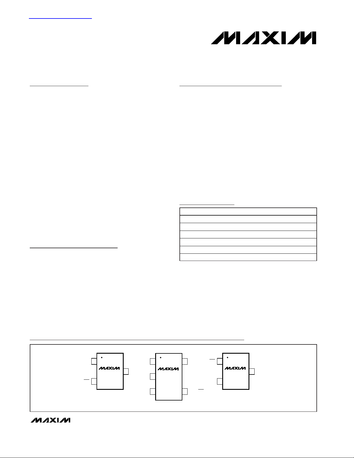
TOP VIEW
(OUT)/OUT
1
3V
CC
GND
MAX6461–
MAX6466
SC70-3
2
GND
(OUT)/OUTGND
15V
CC
N.C.
MAX6461–
MAX6466
SOT23-5
2
34
GND
1
3V
CC
MAX6461–
MAX6466
SOT23-3
2
(OUT)/OUT
( ) ARE FOR THE MAX6462/MAX6465 ONLY
Pin Configurations
Ordering Information
19-2533; Rev 1; 1/03
For pricing, delivery, and ordering information, please contact Maxim/Dallas Direct! at
1-888-629-4642, or visit Maxim’s website at www.maxim-ic.com.
PART TEMP RANGE PIN-PACKAGE
MAX6461XR_ _-T
3 SC70-3
MAX6461UR_ _-T
3 SOT23-3
MAX6461UK_ _-T
5 SOT23-5
MAX6462XR_ _-T
3 SC70-3
MAX6462UR_ _-T
3 SOT23-3
MAX6462UK_ _-T
5 SOT23-5
Ordering Information continued at end of data sheet.
Selector Guide appears at end of data sheet.
The MAX6461–MAX6466 are available in factory-set thresholds
from 1.6V to 5.5V in approximately 100mV increments. Choose
the desired voltage threshold suffix from Table 1 and insert it in
the blank spaces in the part number. There are 30 standard versions with a required order increment of 2500 pieces. Sample
stock generally is held on the standard versions only (Table 2).
Nonstandard versions require a 10k-piece order increment.
Contact factory for availability. All devices available in tape-andreel only.
查询MAX6461供应商
-40°C to +125°C
-40°C to +125°C
-40°C to +125°C
-40°C to +125°C
-40°C to +125°C
-40°C to +125°C
MAX6461–MAX6466
Ultra-Low-Power Voltage Detectors and
µP Supervisory Circuits
2 _______________________________________________________________________________________
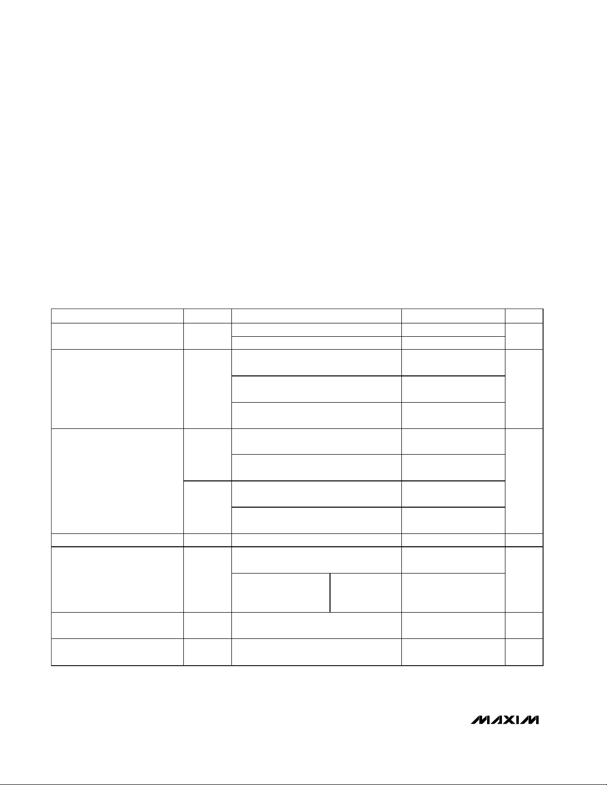
ABSOLUTE MAXIMUM RATINGS
ELECTRICAL CHARACTERISTICS
(VCC= +1.2V to +6V, TA= -40°C to +125°C. Typical values are at TA= +25°C, unless otherwise noted.) (Note1)
Stresses beyond those listed under “Absolute Maximum Ratings” may cause permanent damage to the device. These are stress ratings only, and functional
operation of the device at these or any other conditions beyond those indicated in the operational sections of the specifications is not implied. Exposure to
absolute maximum rating conditions for extended periods may affect device reliability.
(All voltages referenced to GND unless otherwise noted.)
V
CC
, Open-Drain OUT..............................................-0.3V to +7V
Push-Pull OUT/
OUT....................................-0.3V to (VCC+ 0.3V)
Input/Output Current (all pins) ............................................20mA
Output Short Circuit (V
CC
or GND)
Continuous Power Dissipation (T
A
= +70°C)
3-Pin SC70 (derate 2.9mW/°C above +70°C)...........228.6mW
3-Pin SOT23 (derate 4.0mW/°C above +70°C)............320mW
5-Pin SOT23 (derate 7.1mW/°C above +70°C)............571mW
Operating Temperature Range .........................-40°C to +125°C
Junction Temperature......................................................+150°C
Storage Temperature Range .............................-65°C to +150°C
Lead Temperature (soldering, 10s) .................................+300°C
PARAMETER
CONDITIONS
UNITS
TA = 0°C to +125°C16
Operating Voltage Range V
CC
TA = -40°C to 0°C 1.2 6.0
V
V
CC
= 3.6V, TA = -40°C to +125°C,
no load, output not asserted
12
VCC = 5.0V, TA = -40°C to +85°C,
no load, output not asserted
1.3 2.5
VCC Supply Current I
CC
V
CC
= 5.0V, TA = +85°C to +125°C,
no load, output not asserted
3.5
µA
VCC rising, TA = +25°C
(V
TH
+)
(VTH+)
VTH+
V
CC
rising, TA = -40°C to +125°C
(V
TH
+)
(VTH+)
VCC falling, TA = +25°C
(V
TH
-)
(VTH-)
Voltage Threshold
(Note 2)
V
TH
-
V
CC
falling, TA = -40°C to +125°C
(V
TH
-)
(VTH-)
V
Voltage Threshold Hysteresis V
HYST
3 4.5 6 %
VCC falling at 10mV/µs from
(V
TH
-) + 100mV to (V
TH
-) - 100mV
17
Propagation Delay t
P
V
CC
rising at 10mV/µs
from (V
TH
+) - 100mV to
(V
TH
+) + 100mV
MAX6461/
MAX6462/
MAX6463 only
µs
Startup Time
(MAX6461/MAX6462/MAX6463)
µs
Output Timeout Period
(MAX6464/MAX6465/MAX6466)
t
RP
ms
SYMBOL
MIN TYP MAX
V
HYST
= [(VTH+) - (VTH-)] / (VTH-)] × 100%
× 0.985
× 0.975
× 0.985
× 0.975
150 260 430
V
V
TH
TH
100
225
+
-
× 1.015
× 1.025
× 1.015
× 1.025
MAX6461–MAX6466
Ultra-Low-Power Voltage Detectors and
µP Supervisory Circuits
_______________________________________________________________________________________ 3
ELECTRICAL CHARACTERISTICS (continued)
(VCC= +1.2V to +6V, TA= -40°C to +125°C. Typical values are at TA= +25°C, unless otherwise noted.) (Note1)
PARAMETER
SYMBOL
CONDITIONS
MIN
TYP
MAX
UNITS
V
CC
≥ 1.2V, I
SINK
= 1.0mA, OUT asserted 0.3
V
CC
≥ 2.5V, I
SINK
= 4.0mA, OUT asserted 0.3
OUT Output Low (Open Drain or
Push-Pull)
V
OL
V
CC
≥ 4.5V, I
SINK
= 9.0mA, OUT asserted 0.4
V
V
CC
≥ 1.8V, I
SOURCE
= 1.5mA,
OUT not asserted
0.8 ×
V
CC
≥ 2.5V, I
SOURCE
= 3.0mA,
OUT not asserted
0.8 ×
OUT Output High (Push-Pull) V
OH
V
CC
≥ 4.5V, I
SOURCE
= 8.0mA,
OUT not asserted
0.8 ×
V
OUT Output Open-Drain Leakage
Current
I
LKG
OUT not asserted, V
OUT
= +6V
nA
VCC ≥ 1.2V, I
SOURCE
= 200µA,
OUT asserted
0.8 ×
VCC ≥ 1.8V, I
SOURCE
= 1.5mA,
OUT asserted
0.8 ×
VCC ≥ 2.5V, I
SOURCE
= 3.0mA,
OUT asserted
0.8 ×
OUT Output High (Push-Pull) V
OH
VCC ≥ 4.5V, I
SOURCE
= 8.0mA,
OUT asserted
0.8 ×
V
VCC ≥ 2.5V, I
SINK
= 4.0mA,
OUT not asserted
0.3
OUT Output Low (Push-Pull) V
OL
VCC ≥ 4.5V, I
SINK
= 9.0mA,
OUT not asserted
0.4
V
Note 1: 100% production testing done at +25°C. Limits over temperature are guaranteed by design.
Note 2: See Table 1 for V
TH
- and VTH+ values.
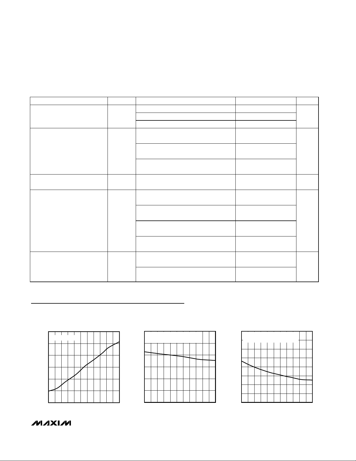
Typical Operating Characteristics
(VCC= 5V, TA= +25°C, unless otherwise noted.)
SUPPLY CURRENT vs. TEMPERATURE
MAX6461 toc01
TEMPERATURE (°C)
SUPPLY CURRENT (µA)
1109580655035205-10-25
1.20
1.25
1.30
1.35
1.40
1.45
1.15
-40 125
VCC = 5V, NO LOAD
PROPAGATION DELAY (RISING)
vs. TEMPERATURE
MAX6461 toc02
TEMPERATURE (°C)
PROPAGATION DELAY (µs)
1109580655035205-10-25
70
80
90
100
110
120
60
-40 125
VCC RISING AT 200mV/µs FROM
((V
TH
+) - 100mV) TO ((VTH+) + 100mV)
PROPAGATION DELAY (FALLING)
vs. TEMPERATURE
MAX6461 toc03
TEMPERATURE (°C)
PROPAGATION DELAY (µs)
1109580655035205-10-25
5
10
15
20
25
30
35
40
0
-40 125
VCC FALLING AT 200mV/µs FROM
((V
TH
-) + 100mV) TO ((VTH-) - 100mV)
V
CC
V
CC
V
CC
V
CC
V
CC
V
CC
V
CC
100

MAX6461–MAX6466
Ultra-Low-Power Voltage Detectors and
µP Supervisory Circuits
4 _______________________________________________________________________________________
Typical Operating Characteristics (continued)
(VCC= 5V, TA= +25°C, unless otherwise noted.)
MAXIMUM VCC TRANSIENT DURATION
vs. V
TH-
THRESHOLD OVERDRIVE
MAX6461 toc04
V
TH-
THRESHOLD OVERDRIVE ((V
TH-
) - VCC) (V)
TRANSIENT DURATION (µs)
0.1
11
12
13
14
15
16
17
18
19
20
10
0.01 1
OUTPUT ASSERTS
ABOVE THIS LINE
MAX6464_ _22
PROPAGATION DELAY VCC RISING
MAX6461 toc05a
20µs/div
100mV/div
AC-COUPLED
1V/div
V
CC
OUT
ACTIVE-HIGH
OUTPUT
MAX6462_ _16
PROPAGATION DELAY VCC FALLING
MAX6461 toc05b
10µs/div
100mV/div
AC-COUPLED
1V/div
V
CC
OUT
ACTIVE-HIGH
OUTPUT
MAX6462_ _16
OUTPUT VOLTAGE HIGH
vs. SOURCE CURRENT
MAX6461 toc06a
SOURCE CURRENT (mA)
OUTPUT VOLTAGE (V)
987654321
4.5
5.0
5.5
6.0
4.0
010
OUTPUT VOLTAGE HIGH
vs. SOURCE CURRENT
MAX6461 toc06b
SOURCE CURRENT (mA)
OUTPUT VOLTAGE (V)
987654321
2.7
2.9
3.1
3.3
3.5
2.5
010
VCC = 3.3V
V
TH
= 2.9V
OUTPUT VOLTAGE LOW
vs. SINK CURRENT
MAX6461 toc07
SINK CURRENT (mA)
OUTPUT VOLTAGE (mV)
986 72 3 4 51
25
50
75
100
125
150
175
200
225
250
275
300
0
010
VCC = 2.7V
V
TH
= 2.9V
NORMALIZED THRESHOLD
vs. TEMPERATURE
MAX6461 toc08
TEMPERATURE (°C)
NORMALIZED THRESHOLD
1109580655035205-10-25
0.99
1.00
1.01
1.02
0.98
-40 125
NORMALIZED OUTPUT TIMEOUT PERIOD
vs. TEMPERATURE
MAX6461 toc09
TEMPERATURE (°C)
NORMALIZED RESET TIMEOUT PERIOD
1109580655035205-10-25
0.99
1.00
1.01
1.02
0.98
-40 125
MAX6466
HYSTERESIS vs. TEMPERATURE
MAX6461 toc10
TEMPERATURE (°C)
% OF V
TH-
1109580655035205-10-25
4.5
5.0
5.5
6.0
4.0
-40 125
MAX6461

Detailed Description
The MAX6461/MAX6462/MAX6463 voltage detectors
and the MAX6464/MAX6465/MAX6466 µP reset supervisory circuits monitor battery, power-supply, and system
voltages from +1.6V to +5.5V. These devices consume
only 1µA of supply current with a 3.6V supply voltage.
Whenever V
CC
falls below the internal VTH- threshold,
the output is asserted and remains asserted until V
CC
rises above V
TH+ (VTH+
= VTH- × 1.05). All devices have
±2.5% threshold accuracy over temperature and offer
protection to short voltage transients. These devices are
ideal for low-cost and space-critical applications
because they do not require external components for
proper operation.
MAX6461–MAX6466
Ultra-Low-Power Voltage Detectors and
µP Supervisory Circuits
_______________________________________________________________________________________ 5
Pin Description
PIN
MAX6461–MAX6466
SOT23-3
NAME FUNCTION
OUT
Detector Output for the MAX6461/MAX6462/MAX6463: Push-pull (active-low or
active-high) and open-drain (active-low) options. OUT is asserted low when the
monitored input (V
CC
) drops below the internal V
TH-
threshold and remains low
until the monitored input exceeds the internal V
TH+
threshold. OUT is asserted
high when the monitored input (V
CC
) drops below the internal V
TH-
threshold and
remains high until the monitored input exceeds the internal V
TH+
threshold. The
open-drain output OUT requires an external pullup resistor. Output for the
MAX6464/MAX6465/MAX6466: Push-pull (active-low or active-high) and opendrain (active-low) options.
124
OUT
OUT is asserted low when the monitored input (V
CC
) drops below the internal
V
TH-
threshold and remains low for at least 150ms after the monitored input
exceeds the internal V
TH+
threshold. OUT is asserted high when the monitored
input (V
CC
) drops below the internal V
TH-
threshold and remains high for at least
150ms after the monitored input exceeds the internal V
TH+
threshold. The open-
drain output OUT requires an external pullup resistor.
2 1 2, 3 GND Ground. In the SOT23-5 package, both pins must be grounded.
335VCCSupply Voltage and Monitored Voltage Input
—— 1 N.C. No Connection
Functional Diagram
SC70-3 SOT23-5
V
CC
R1
R2
R3
1.23V
MAX6461–
MAX6466
RESET
TIMEOUT
OUTPUT
STAGE
OUT

MAX6461–MAX6466
Applications Information
Interfacing to Different Logic Voltage
Components
The MAX6463 and MAX6466’s active-low, open-drain output versions can be used to interface with a different logic
voltage than VCC, as shown in Figure 1. This output structure sinks current when OUT is asserted. Connect a
pullup resistor from OUT to any supply from 0 to 6V.
Select a resistor value large enough to allow a valid logic
low (see the Electrical Characteristics) and small enough
to register a logic high while supplying all input current
and leakage paths connected to the OUT pin.
Hysteresis
The MAX6461–MAX6466 feature internal hysteresis that
creates two trip points: one for rising supply voltage
and one for falling supply voltage. The hysteresis prevents the output from oscillating (chattering) when V
CC
is near the voltage threshold.
Transients Immunity
These devices are relatively immune to short-duration
and falling VCCtransients (glitches). The Typical
Operating Characteristics show the Maximum Transient
Duration vs. Threshold Overdrive graph, for which OUT
is not asserted. The graph shows the maximum pulse
width that a falling VCCtransient typically might have
before the devices are asserted. As the amplitude of
the transient increases, the maximum allowable pulse
width decreases.
Ensuring Valid Output Down to 0V
When VCCfalls below 1V, the MAX6461/MAX6464 output sinking capability is reduced. Therefore, highimpedance CMOS logic inputs connected to OUT can
drift to undetermined voltages. This presents no problem in most applications, because most circuitry is
inoperative when VCCis below 1V. In applications
where OUT must be valid down to ground, add a pulldown resistor to ground so any stray leakage currents
flow to ground, holding OUT low. Select a resistor large
enough not to load OUT and small enough to pull OUT
to ground. For most applications, 100kΩ does not load
OUT and pulls OUT to ground.
Ultra-Low-Power Voltage Detectors and
µP Supervisory Circuits
6 _______________________________________________________________________________________
DC/DC
CONVERTER
OUT
MAX6463
MAX6466
µP
SUSPEND
V
CC
OUTIN
V
CC
3.6V
Li+
Figure 1. Interfacing to Different Logic Voltage Components

MAX6461–MAX6466
Ultra-Low-Power Voltage Detectors and
µP Supervisory Circuits
_______________________________________________________________________________________ 7
Table 1a. MAX6461–MAX6466 Lower Trip Threshold (VTH-) Voltage Options
VOLTAGE THRESHOLD, V
TH-
TA = +25°CT
A
= -40°C to +125°C
SUFFIX
V
TH-
(min) V
TH-
(typ) V
TH-
(max) V
TH-
(min) V
TH-
(max)
16 1.576 1.600 1.624 1.560 1.640
17 1.675 1.700 1.726 1.658 1.743
18 1.773 1.800 1.827 1.755 1.845
19 1.872 1.900 1.929 1.853 1.948
20 1.970 2.000 2.030 1.950 2.050
21 2.069 2.100 2.132 2.048 2.153
22 2.167 2.200 2.233 2.145 2.255
23 2.266 2.300 2.335 2.243 2.358
24 2.364 2.400 2.436 2.340 2.460
25 2.463 2.500 2.538 2.438 2.563
26 2.561 2.600 2.639 2.535 2.665
27 2.660 2.700 2.741 2.633 2.768
28 2.758 2.800 2.842 2.730 2.870
29 2.857 2.900 2.944 2.828 2.973
30 2.955 3.000 3.045 2.925 3.075
31 3.054 3.100 3.147 3.023 3.178
32 3.152 3.200 3.248 3.120 3.280
33 3.251 3.300 3.350 3.218 3.383
34 3.349 3.400 3.451 3.315 3.485
35 3.448 3.500 3.553 3.413 3.588
36 3.546 3.600 3.654 3.510 3.690
37 3.645 3.700 3.756 3.608 3.793
38 3.743 3.800 3.857 3.705 3.895
39 3.842 3.900 3.959 3.803 3.998
40 3.940 4.000 4.060 3.900 4.100
41 4.039 4.100 4.162 3.998 4.203
42 4.137 4.200 4.263 4.095 4.305
43 4.236 4.300 4.365 4.193 4.408
44 4.334 4.400 4.466 4.290 4.510
45 4.433 4.500 4.568 4.388 4.613
46 4.531 4.600 4.669 4.485 4.715
47 4.630 4.700 4.771 4.583 4.818
48 4.728 4.800 4.872 4.680 4.920
49 4.827 4.900 4.974 4.778 5.023
50 4.925 5.000 5.075 4.875 5.125
51 5.024 5.100 5.177 4.973 5.228
52 5.122 5.200 5.278 5.070 5.330
53 5.221 5.300 5.380 5.168 5.433
54 5.319 5.400 5.481 5.265 5.535
55 5.418 5.500 5.583 5.363 5.638

MAX6461–MAX6466
Ultra-Low-Power Voltage Detectors and
µP Supervisory Circuits
8 _______________________________________________________________________________________
Table 1b. MAX6461–MAX6466 Upper Trip Threshold (VTH+) Voltage Options
VOLTAGE THRESHOLD, V
TH+
TA = +25°CT
A
= -40°C to +125°C
SUFFIX
V
TH+
(min) V
TH+
(typ) V
TH+
(max) V
TH+
(min) V
TH+
(max)
16 1.647 1.672 1.697 1.630 1.714
17 1.750 1.777 1.803 1.732 1.821
18 1.853 1.881 1.909 1.834 1.928
19 1.956 1.986 2.015 1.936 2.035
20 2.059 2.090 2.121 2.038 2.142
21 2.162 2.195 2.227 2.140 2.249
22 2.265 2.299 2.333 2.242 2.356
23 2.367 2.404 2.440 2.343 2.464
24 2.470 2.508 2.546 2.445 2.571
25 2.573 2.613 2.652 2.547 2.678
26 2.676 2.717 2.758 2.649 2.785
27 2.779 2.822 2.864 2.751 2.892
28 2.882 2.926 2.970 2.853 2.999
29 2.985 3.031 3.076 2.955 3.106
30 3.088 3.135 3.182 3.057 3.213
31 3.191 3.240 3.288 3.159 3.320
32 3.294 3.344 3.394 3.260 3.428
33 3.397 3.449 3.500 3.362 3.535
34 3.500 3.553 3.606 3.464 3.642
35 3.603 3.658 3.712 3.566 3.749
36 3.706 3.762 3.818 3.668 3.856
37 3.809 3.867 3.924 3.770 3.963
38 3.911 3.971 4.031 3.872 4.070
39 4.014 4.076 4.137 3.974 4.177
40 4.117 4.180 4.243 4.076 4.285
41 4.220 4.285 4.349 4.177 4.392
42 4.323 4.389 4.455 4.279 4.499
43 4.426 4.494 4.561 4.381 4.606
44 4.529 4.598 4.667 4.483 4.713
45 4.632 4.703 4.773 4.585 4.820
46 4.735 4.807 4.879 4.687 4.927
47 4.838 4.912 4.985 4.789 5.034
48 4.941 5.016 5.091 4.891 5.141
49 5.044 5.121 5.197 4.992 5.249
50 5.147 5.225 5.303 5.094 5.356
51 5.250 5.330 5.409 5.196 5.463
52 5.352 5.434 5.516 5.298 5.570
53 5.455 5.539 5.622 5.400 5.677
54 5.558 5.643 5.728 5.502 5.784
55 5.661 5.748 5.834 5.604 5.891

MAX6461–MAX6466
Ultra-Low-Power Voltage Detectors and
µP Supervisory Circuits
_______________________________________________________________________________________ 9
Table 2. Standard Versions Table
PART
TOP MARK
(SC70)
MAX6461XR16-T AMB
MAX6461XR22-T AMC
MAX6461XR26-T AMD
MAX6461XR29-T AKV
MAX6461XR46-T AME
MAX6462XR16-T AKW
MAX6462XR22-T AMF
MAX6462XR26-T AMG
MAX6462XR29-T AMH
MAX6462XR46-T AMI
MAX6463XR16-T AMJ
MAX6463XR22-T AMK
MAX6463XR26-T AML
MAX6463XR29-T AMM
MAX6463XR46-T AMN
Selector Guide
PART
PUSH-PULL
OUT
PUSH-PULL
OUT
OPEN-DRAIN
OUT
TYPICAL
PROPAGATION
DELAY (µs)
MINIMUM TIMEOUT
PERIOD (ms)
MAX6461 ✔ ——14 —
MAX6462 — ✔ — 14 —
MAX6463 ——✔ 14 —
MAX6464 ✔ ———150
MAX6465 — ✔ ——150
MAX6466 ——✔ — 150
PART
MAX6464XR16-T AMO
MAX6464XR22-T AMP
MAX6464XR26-T AMQ
MAX6464XR29-T AMR
MAX6464XR46-T AMS
MAX6465XR16-T AMT
MAX6465XR22-T AMU
MAX6465XR26-T AMV
MAX6465XR29-T AMW
MAX6465XR46-T AKZ
MAX6466XR16-T AMX
MAX6466XR22-T AMY
MAX6466XR26-T AMZ
MAX6466XR29-T ALA
MAX6466XR46-T ALB
TOP MARK
(SC70)

MAX6461–MAX6466
Ultra-Low-Power Voltage Detectors and
µP Supervisory Circuits
Maxim cannot assume responsibility for use of any circuitry other than circuitry entirely embodied in a Maxim product. No circuit patent licenses are
implied. Maxim reserves the right to change the circuitry and specifications without notice at any time.
10 ____________________Maxim Integrated Products, 120 San Gabriel Drive, Sunnyvale, CA 94086 408-737-7600
© 2003 Maxim Integrated Products Printed USA is a registered trademark of Maxim Integrated Products.
Chip Information
TRANSISTOR COUNT: 581
PROCESS: BiCMOS
Package Information
For the latest package outline information, go to
www.maxim-ic.com/packages
.)
Ordering Information (continued)
PART TEMP RANGE PIN-PACKAGE
MAX6463XR_ _-T
3 SC70-3
MAX6463UR_ _-T
3 SOT23-3
MAX6463UK_ _-T
5 SOT23-5
MAX6464XR_ _-T
3 SC70-3
MAX6464UR_ _-T
3 SOT23-3
MAX6464UK_ _-T
5 SOT23-5
MAX6465XR_ _-T
3 SC70-3
MAX6465UR_ _-T
3 SOT23-3
MAX6465UK_ _-T
5 SOT23-5
MAX6466XR_ _-T
3 SC70-3
MAX6466UR_ _-T
3 SOT23-3
MAX6466UK_ _-T
5 SOT23-5
The MAX6461–MAX6466 are available in factory-set thresholds
from 1.6V to 5.5V in approximately 100mV increments. Choose
the desired voltage threshold suffix from Table 1 and insert it in
the blank spaces in the part number. There are 30 standard versions with a required order increment of 2500 pieces. Sample
stock generally is held on the standard versions only (Table 2).
Nonstandard versions require a 10k-piece order increment.
Contact factory for availability. All devices available in tape-andreel only.
-40°C to +125°C
-40°C to +125°C
-40°C to +125°C
-40°C to +125°C
-40°C to +125°C
-40°C to +125°C
-40°C to +125°C
-40°C to +125°C
-40°C to +125°C
-40°C to +125°C
-40°C to +125°C
-40°C to +125°C
 Loading...