

General Description
The MAX6453–MAX6456 are low-power, dual-voltage
µP supervisors featuring separate VCCreset and manual reset outputs. The dual outputs support both softsystem reset (interrupt) and hard-system reset (reboot)
functions. The reset output asserts when any of the
monitored voltages falls below its specified threshold
and remains asserted for the reset timeout (140ms min)
after all voltages exceed their respective reset thresholds. All devices are offered with nine factory-fixed
reset thresholds for monitoring primary system voltages
(VCC) from 1.8V to 5V and an adjustable reset input for
monitoring a secondary system voltage down to 0.63V.
Each device has a manual reset input, a VCCreset output, and a manual reset output. The MAX6453/
MAX6454 manual reset output asserts when the manual
reset input is low. It remains asserted for the manual
reset timeout period (140ms min) after the manual reset
input transitions high. The MAX6453/MAX6354 manual
reset input controls only the manual reset output and
does not affect the VCCreset output.
The manual reset input of the MAX6455/MAX6456 controls both the manual reset and VCCreset outputs. When
the manual reset input is low for less than 3.3s (typ), only
the manual reset output asserts and remains asserted for
the manual reset timeout period (140ms min) after the
manual reset input transitions high. If the manual reset
input is low for at least 3.3s (typ), the reset output also
asserts and remains asserted for the reset timeout period (140ms min) after the manual reset input transitions
high. This enhanced feature allows the implementation of
a soft/hard-system reset combination.
The MAX6453/MAX6455 have active-low push-pull
reset and manual reset outputs, and the MAX6454/
MAX6456 have active-low open-drain reset and manual
reset outputs. All devices are available in small SOT236 packages and are fully specified over the extended
temperature range (-40°C to +85°C).
Applications
Set-Top Boxes
Consumer Electronics
DVD Players
Modems
MP3 Players
Industrial Equipment
Automotive
Medical Devices
Features
♦ Precision Factory-Set Reset Thresholds From
1.6V to 4.6V
♦ Adjustable Threshold to Monitor Voltages Down
to 0.63V
♦ Manual Reset Input with Extended 3.36s Setup
Period
♦ Immune to Short Voltage Transients
♦ Low 6µA Supply Current
♦ Guaranteed Valid Reset Down to V
CC
= 1.0V
♦ Active-Low RESET (Push-Pull or Open-Drain)
Outputs
♦ 140ms (min) Reset Timeout Period
♦ Small SOT Package
MAX6453–MAX6456
µP Supervisors with Separate V
CC
Reset and
Manual Reset Outputs
________________________________________________________________ Maxim Integrated Products 1
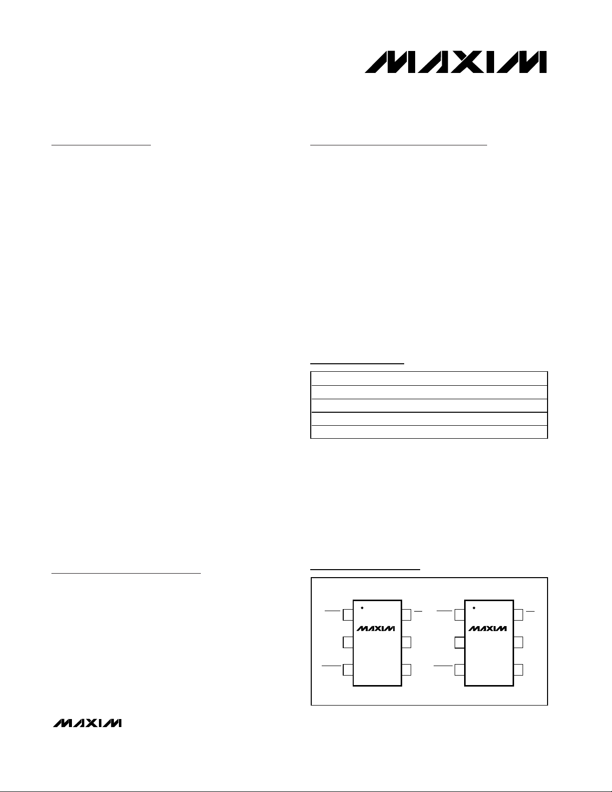
Pin Configurations
Ordering Information
19-2637; Rev 1; 4/03
For pricing, delivery, and ordering information, please contact Maxim/Dallas Direct! at
1-888-629-4642, or visit Maxim’s website at www.maxim-ic.com.
Note: The “_” is a placeholder for the threshold voltage level of
the devices. A desired threshold level is set by the part number suffix found in Table 1. All devices are available in tapeand-reel only. There is a 2500-piece minimum order increment
for standard versions (Table 2). Sample stock is typically held
on standard versions only. Nonstandard versions require a
minimum order increment of 10,000 pieces. Contact factory for
availability.
Selector Guide appears at end of data sheet.
PART TEMP RANGE PIN-PACKAGE
MAX6453UT_ _S-T -40°C to +85°C 6 SOT23-6
MAX6454UT_ _S-T -40°C to +85°C 6 SOT23-6
MAX6455UT_ _S-T -40°C to +85°C 6 SOT23-6
MAX6456UT_ _S-T -40°C to +85°C 6 SOT23-6
TOP VIEW
RESET
GND
MROUT
16MR
MAX6453
2
MAX6454
34
SOT23-6
5 RSTIN
V
CC
16MR
RESET
GND
2
34
MROUT
MAX6455
MAX6456
SOT23-6
5 RSTIN
V
CC
MAX6453–MAX6456
µP Supervisors with Separate V
CC
Reset and
Manual Reset Outputs
2 _______________________________________________________________________________________
ABSOLUTE MAXIMUM RATINGS
Stresses beyond those listed under “Absolute Maximum Ratings” may cause permanent damage to the device. These are stress ratings only, and functional
operation of the device at these or any other conditions beyond those indicated in the operational sections of the specifications is not implied. Exposure to
absolute maximum rating conditions for extended periods may affect device reliability.
(All voltages referenced to GND)
V
CC
..........................................................................-0.3V to +6V
Open-Drain RESET, MROUT ....................................-0.3V to +6V
Push-Pull RESET, MROUT..........................-0.3V to (V
CC
+ 0.3V)
MR, RSTIN ...............................................................-0.3V to +6V
Input Current, All Pins.......................................................±20mA
Continuous Power Dissipation (T
A
= +70°C)
6-Pin SOT23 (derate 8.7mW/°C above +70°C).............696mW
Operating Temperature Range .......................... -40°C to +85°C
Junction Temperature......................................................+150°C
Storage Temperature Range .............................-65°C to +150°C
Lead Temperature (soldering, 10s) .................................+300°C
ELECTRICAL CHARACTERISTICS
(VCC= 1.0V to 5.5V, TA= -40°C to +85°C, unless otherwise specified. Typical values are at TA= +25°C.) (Note 1)
Operating Voltage Range V
VCC Supply Current I
VCC Reset Threshold V
Reset Threshold Tempco 60 ppm/°C
Reset Threshold Hysteresis 2 × V
RSTIN Threshold V
RSTIN Threshold Hysteresis V
RSTIN Input Current I
RSTIN to Reset Output Delay V
Reset Timeout Period t
VCC to RESET Output Delay t
MR Minimum Setup Period
(Pulse Width)
MR Minimum Input Pulse RESET asserted, MAX6455/MAX6456 2.24 3.36 4.48 s
MR Glitch Rejection 100 ns
MR to MROUT Delay 200 ns
Manual Reset Timeout Period t
PARAMETER SYMBOL CONDITIONS MIN TYP MAX UNITS
CC
CC
TH
TH-RSTIN
HYST
RSTIN
RP
RD
t
MR
MRP
VCC = 5.5V, no load 7 20
VCC = 3.6V, no load 6 16
46 4.50 4.63 4.75
44 4.25 4.38 4.50
31 3.00 3.08 3.15
29 2.85 2.93 3.00
26 2.55 2.63 2.70
23 2.25 2.32 2.38
22 2.12 2.19 2.25
17 1.62 1.67 1.71
16 1.52 1.58 1.62
TA = 0°C to +85°C 0.615 0.630 0.645
TA = -40°C to +85°C 0.610 0.650
falling at 1mV/µs 15 µs
RSTIN
VCC falling at 1mV/µs 20 µs
MR to MROUT 1µs
1.0 5.5 V
TH
2.5 mV
-25 +25 nA
140 210 280 ms
140 210 280 ms
µA
V
mV
V
MAX6453–MAX6456
µP Supervisors with Separate V
CC
Reset and
Manual Reset Outputs
_______________________________________________________________________________________ 3
ELECTRICAL CHARACTERISTICS (continued)
(VCC= 1.0V to 5.5V, TA= -40°C to +85°C, unless otherwise specified. Typical values are at TA= +25°C.) (Note 1)
Note 1: Devices production tested at 25°C. Overtemperature limits are guaranteed by design.
MR to VCC Pullup Impedance 25 50 75 kΩ
RESET, MROUT Output Low
(Open Drain or Push-Pull)
RESET, MROUT Output High
(Push-Pull)
RESET, MROUT Output
Open-Drain Leakage Current
MR Input Low Voltage V
MR Input High Voltage V
PARAMETER SYMBOL CONDITIONS MIN TYP MAX UNITS
V
V
I
LKG
OL
OH
IL
IH
VCC ≥ 1.00V, I
asserted
VCC ≥ 1.20V, I
asserted
VCC ≥ 2.55V, I
asserted
VCC ≥ 4.25V, I
asserted
VCC ≥ 1.80V, I
outputs deasserted
VCC ≥ 3.15V, I
outputs deasserted
VCC ≥ 4.75V, I
outputs deasserted
Outputs deasserted 1 µA
= 50µA, outputs
SINK
= 100µA, outputs
SINK
= 1.2mA, outputs
SINK
= 3.2mA, outputs
SINK
= 200µA,
SOURCE
= 500µA,
SOURCE
= 800µA,
SOURCE
0.8 × V
0.8 × V
0.8 × V
0.7 × V
CC
CC
CC
CC
0.3
0.3
0.3
0.4
0.3 × V
CC
V
V
V
V

MAX6453–MAX6456
µP Supervisors with Separate V
CC
Reset and
Manual Reset Outputs
4 _______________________________________________________________________________________
Typical Operating Characteristics
(VCC= 3.3V, TA = +25°C, unless otherwise noted.)
SUPPLY CURRENT
vs. SUPPLY VOLTAGE
MAX6453 toc01
SUPPLY VOLTAGE (V)
SUPPLY CURRENT (µA)
5.04.53.5 4.02.0 2.5 3.01.5
1
2
3
4
5
6
7
8
9
0
1.0 5.5
TA = +85°C
T
A
= -40°C
TA = +25°C
NORMALIZED RESET TIMEOUT PERIOD
vs. TEMPERATURE
MAX6453 toc02
TEMPERATURE (°C)
NORMALIZED TIMEOUT PERIOD
603510-15
0.96
0.97
0.98
0.99
1.00
1.01
1.02
1.03
1.04
1.05
0.95
-40 85
MAXIMUM TRANSIENT DURATION
vs. RESET THRESHOLD OVERDRIVE
MAX6453 toc03
RESET THRESHOLD OVERDRIVE (mV)
TRANSIENT DURATION (µs)
800600400200
50
100
150
200
250
0
0 1000
RESET OCCURS
ABOVE THE CURVE
VTH = 4.4V
NORMALIZED VCC RESET THRESHOLD
vs. TEMPERATURE
MAX6453 toc04
TEMPERATURE (°C)
NORMALIZED V
CC
RESET THRESHOLD
603510-15
0.98
0.99
1.00
1.01
1.02
1.03
0.97
-40 85
V
CC
TO RESET DELAY
vs. TEMPERATURE
MAX6453 toc05
TEMPERATURE (°C)
V
CC
TO RESET DELAY (µs)
603510-15
20.4
20.8
21.2
21.6
22.0
22.4
22.8
23.2
23.6
24.0
20.0
-40 85
V
CC
FALLING AT 1mV/µs
RSTIN TO RESET DELAY
vs. TEMPERATURE (RSTIN FALLING)
MAX6453 toc06
TEMPERATURE (°C)
RSTIN TO RESET DELAY (µs)
603510-15
20.4
20.8
21.2
21.6
22.0
22.4
22.8
23.2
23.6
24.0
20.0
-40 85
RSTIN FALLING AT 1mV/µs
MANUAL RESET TO MROUT AND
RESET DELAY (MAX6455/MAX6456)
MAX6453 toc07
TIME (1s/div)
MR (5V/div)
MROUT (5V/div)
RESET (5V/div)
V
CC
= 5V
VCC TO RESET DELAY
MAX6453 toc08
TIME (100µs/div)
V
CC
(100mV/div)
RESET (2V/div)
V
CC
= 4.5V
V
TH
= 4.392V
V
CC
= 4.3V

MAX6453–MAX6456
µP Supervisors with Separate V
CC
Reset and
Manual Reset Outputs
_______________________________________________________________________________________ 5
Pin Description
PIN
MAX6453
MAX6454
1 —
— 1
2 2 GND Ground
33MROUT
44V
5 5 RSTIN
6 —
— 6
MAX6455
MAX6456
NAME FUNCTION
RESET
CC
MR
Active-Low Push-Pull or Open-Drain Output. RESET changes from high to low when
V
or RSTIN drops below its selected reset threshold. RESET remains low for the
CC
140ms (min) reset timeout period after all monitored power-supply inputs exceed their
selected reset thresholds. MR does not affect RESET output. For open-drain outputs,
connect to an external pullup resistor.
Active-Low Push-Pull or Open-Drain Output. RESET changes from high to low when
or RSTIN drops below its selected reset threshold. RESET remains low for the
V
CC
140ms (min) reset timeout period after all monitored power-supply inputs exceed their
selected reset thresholds. RESET changes from high to low after MR input is held low
for the 3.36s (typ) setup period and deasserts 140ms (min) after MR deasserts. For
open-drain outputs, connect to an external pullup resistor.
Manual Reset Push-Pull or Open-Drain Output. MROUT asserts immediately after MR is
pulled low. MROUT remains low for 140ms (min) after MR is deasserted. For opendrain outputs, connect to an external pullup resistor.
VCC Voltage Input. Power supply and input for the primary microprocessor voltage
reset monitor.
Reset Input. High-impedance input to the adjustable reset comparator. Connect RSTIN
to the center point of an external resistor divider to set the threshold of the externally
monitored voltage.
Manual Reset Input. Internal 50kΩ pullup to V
MROUT. MR does not affect RESET output.
Manual Reset Input. Internal 50kΩ pullup to V
MROUT. RESET changes from high to low after MR input is held low for the 3.36s (typ)
setup period.
Pull MR low to immediately assert
CC.
Pull MR low to immediately assert
CC.

MAX6453–MAX6456
µP Supervisors with Separate V
CC
Reset and
Manual Reset Outputs
6 _______________________________________________________________________________________
Detailed Description
Reset Output
The reset output is typically connected to the reset
input of a microprocessor (µP). A µP’s reset input starts
or restarts the µP in a known state. The MAX6453–
MAX6456 µP supervisory circuits provide the reset
logic to prevent code-execution errors during powerup, power-down and brownout conditions (see the
Typical Operating Circuit).
RESET changes from high to low whenever the monitored voltage (RSTIN or VCC) drops below the reset
threshold voltages. When V
RSTIN
and VCCexceed their
respective reset threshold voltages, RESET remains low
for the reset timeout period, and then goes high. RESET
changes from high to low after MR input is held low for
the 3.36s (typ) setup period and deasserts 140ms (min)
after MR deasserts.
RESET is guaranteed to be in the proper output logic
state for VCCinputs ≥ 1V. For applications requiring valid
reset logic when VCCis less than 1V, see the Ensuring a
Valid
RESET
Output Down to VCC= 0V section.
Manual Reset
The MAX6453/MAX6454 contain a manual reset output
(MROUT) that asserts low immediately after driving MR
low and remains low for the reset timeout period after
MR goes high (Figure 1). The pushbutton manual reset
has no effect on the RESET output. MROUT output can
be used to drive an NMI (nonmaskable interrupt) on the
processor to save valuable data.
The MAX6455/MAX6456’s MROUT is asserted immediately upon driving MR low. Driving MR low for longer
than the 3.36s (typ) setup period asserts RESET. When
MR is deasserted, MROUT and RESET remain asserted
low for the reset timeout period after MR goes high
(Figure 2).
Adjustable Input Voltage (RSTIN)
The MAX6453–MAX6456 monitor the voltage on RSTIN
using an adjustable reset threshold set with an external
resistor voltage divider (Figure 3). Use the following formula to calculate the externally monitored voltage
(V
MON-TH
):
V
MON-TH
= V
TH-RSTIN
✕ (R1 +R2) / R2
where V
MON_TH
is the desired reset threshold voltage
and V
TH-RSTIN
is the reset input threshold (0.63V).
Resistors R1 and R2 can have very high values to minimize current consumption due to low leakage currents.
Set R2 to some conveniently high value (250kΩ, for
example) and calculate R1 based on the desired reset
threshold voltage, using the following formula:
R1 = R2 ✕ (V
MON_TH
/ VTH- 1)Ω
Figure 2. MAX6455/MAX6456 Timing Diagram
Figure 1. MAX6453/MAX6454 Timing Diagram
MR
MROUT
210ms
LONG SETUP PERIOD, 3.36s
MR
MROUT
RESET
210ms

MAX6453–MAX6456
µP Supervisors with Separate V
CC
Reset and
Manual Reset Outputs
_______________________________________________________________________________________ 7
Applications Information
Interrupt Before Reset
To minimize data loss and speed system recovery/test,
many applications interrupt the processor or reset only
portions of the system before a processor hard reset is
asserted. The extended setup time of the MAX6455/
MAX6456 MR input allows the same pushbutton (Figure
4) to control both the interrupt and hard reset functions.
If the pushbutton is closed for less than 3.36s (typ), the
processor is only interrupted (MROUT). If the system
still does not respond properly, the pushbutton can be
closed for the full extended setup period (3.36s typ) to
hard reset the processor (RESET). If desired, connect a
LED to the RESET output to turn off (or on) to signify
when the pushbutton is closed long enough for a hard
reset (the same LED can be used as the front panel
power-on display).
Interfacing to Other Voltages
for Logic Compatibility
The open-drain RESET output can be used to interface
to a µP with other logic levels. As shown in Figure 5, the
open-drain output can be connected to voltages from 0
to 6V.
Generally, the pullup resistor connected to the RESET
connects to the supply voltage being monitored at the
IC’s V
CC
pin. However, some systems might use the
open-drain output to level-shift from the monitored supply to reset circuitry powered by some other supply
(Figure 5). Keep in mind that as the supervisor’s V
CC
decreases toward 1V, so does the IC’s ability to sink
current at RESET (RESET is pulled high as VCCdecays
toward 0). The voltage where this occurs depends on
the pullup resistor value and the voltage to which it is
connected.
Ensuring a Valid
RESET
Down to VCC= 0V
(Push-Pull
RESET
)
When VCCfalls below 1V, RESET current-sinking capabilities decline drastically. The high-impedance CMOSlogic inputs connected to RESET can drift to
undetermined voltages. This presents no problem in
most applications, because most µPs and other circuitry do not operate with V
CC
below 1V.
In applications where RESET must be valid down to 0V,
add a pulldown resistor between RESET and GND for
the push/pull outputs. The resistor sinks any stray leakage currents, holding RESET low (Figure 6). The value
of the pulldown resistor is not critical; 100kΩ is large
enough not to load RESET and small enough to pull
RESET to ground. The external pulldown cannot be
used with the open-drain reset outputs.
Transient Immunity
In addition to issuing a reset to the µP during power-up,
power-down and brownout conditions, these supervisors
are relatively immune to short duration falling transients
(glitches). The graph Maximum Transient Duration vs.
Reset Threshold Overdrive in the Typical Operating
Characteristics section shows this relationship.
The area below the curves of the graph is the region in
which these devices typically do not generate a reset
pulse. This graph was generated using a negative
going pulse applied to VCC, starting above the actual
reset threshold (VTH) and ending below it by the magnitude indicated (reset-threshold overdrive). As the magnitude of the transient increases (V
CC
goes further
below the reset threshold), the maximum allowable
pulse width decreases. Typically, a VCCtransient that
goes 100mV below the reset threshold and lasts 20µs
or less does not cause a reset pulse to be issued.
Figure 3. Calculating The Monitored Threshold Voltages
V
MON_TH
R1
R2
= 0.63 x (R1 + R2) / R2
V
MON_TH
RSTIN
GND
MAX6453
MAX6455
V
RESET
CC
V
CC

MAX6453–MAX6456
µP Supervisors with Separate V
CC
Reset and
Manual Reset Outputs
8 _______________________________________________________________________________________
Figure 5. Interfacing to Other Voltage Levels
Figure 6. Ensuring
RESET
Valid to VCC= 0
Figure 4. Interrupt Before Reset Application Circuit
Functional Diagram
+3.3V
+1.5V
CORE SUPPLY
V
CC
RESET
RESET
MAX6455
RSTIN
GND
MROUT
MR
LED
NMI
PUSHBUTTON SWITCH
CLOSE FOR IMMEDIATE SYSTEM INTERRUPT
CLOSE FOR >3.36s FOR SYSTEM RESET
µ
SUPPLY
P
5V
I/O
V
CC
MAX6454
100kΩ
3.3V
V
µ
CC
P
MAX6456
RESET
GND
RESET
GND
V
CC
V
CC
V
CC
MAX6453
MAX6455
GND
RESET
100kΩ
RSTIN
V
CC
1.23V
GND
0.63V
V
CC
MR
MAX6453–
MAX6456
RESET
TIMOUT PERIOD
(210ms typ)
MR-TO-RESET
SETUP PERIOD
(3.36s typ)
MAX6455/MAX6456
MROUT
TIMOUT PERIOD
(210ms typ)
RESET
MROUT

MAX6453–MAX6456
µP Supervisors with Separate V
CC
Reset and
Manual Reset Outputs
_______________________________________________________________________________________ 9
Table 1. Reset Voltage Threshold
Table 2. Standard Versions Table
*Other timing options may be available. Contact factory for availability.
Selector Guide
MAX6453
µ
P
V
CC
RSTIN
RESET
NMI
I/O
SUPPLY
CORE SUPPLY
+3.3V
+1.5V
RESET
MROUT
GND
MR
GND
Typical Operating Circuit
Chip Information
TRANSISTOR COUNT: 1384
PROCESS: BiCMOS
PART NO.
SUFFIX
( _ _ )
46 4.625
44 4.375
31 3.075
29 2.925
26 2.625
23 2.313
22 2.188
17 1.665
16 1.575
VCC NOMINAL
THRESHOLD (V)
VOLTAGE
PART
MAX6453UT16S ABOG MAX6455UT16S ABOL
MAX6453UT23S ABOH MAX6455UT23S ABOM
MAX6453UT26S ABOI MAX6455UT26S ABON
MAX6453UT29S ABOJ MAX6455UT29S ABOO
MAX6453UT46S ABOK MAX6455UT46S ABER
MAX6454UT16S ABOP MAX6456UT16S ABES
MAX6454UT23S ABEQ MAX6456UT23S ABOT
MAX6454UT26S ABOQ MAX6456UT26S ABOU
MAX6454UT29S ABOR MAX6456UT29S ABOV
MAX6454UT46S ABOS MAX6456UT46S ABOW
TOP
MARK
PART MR TO RESET DELAY MR ASSERTION
MAX6453 — MROUT ✓ —
MAX6454 — MROUT — ✓
MAX6455 3.36s MROUT and RESET ✓ —
MAX6456 3.36s MROUT and RESET — ✓
MROUT AND RESET
PUSH-PULL OUTPUT
MROUT AND RESET
OPEN-DRAIN OUTPUT
PART
TOP
MARK

MAX6453–MAX6456
µP Supervisors with Separate V
CC
Reset and
Manual Reset Outputs
Maxim cannot assume responsibility for use of any circuitry other than circuitry entirely embodied in a Maxim product. No circuit patent licenses are
implied. Maxim reserves the right to change the circuitry and specifications without notice at any time.
10 ____________________Maxim Integrated Products, 120 San Gabriel Drive, Sunnyvale, CA 94086 408-737-7600
© 2003 Maxim Integrated Products Printed USA is a registered trademark of Maxim Integrated Products.
Package Information
(The package drawing(s) in this data sheet may not reflect the most current specifications. For the latest package outline information,
go to www.maxim-ic.com/packages
.)
6LSOT.EPS
PACKAGE OUTLINE, SOT-23, 6L
21-0058
1
F
1
 Loading...