

General Description
The MAX6406–MAX6411 is a family of ultra-low power
circuits used for monitoring battery, power-supply, and
regulated system voltages. Each detector contains a
precision bandgap reference comparator and is
trimmed to specified trip threshold voltages. These
devices provide excellent circuit reliability and low cost
by eliminating external components and adjustments
when monitoring system voltages from 2.5V to 5.0V. A
manual reset input is also included.
The MAX6406–MAX6411 assert a signal whenever the
VCCsupply voltage falls below a preset threshold.
These devices are differentiated by their output logic
configurations and preset threshold voltages. The
MAX6406/MAX6409 (push-pull) and the MAX6408/
MAX6411 (open-drain) have an active-low output (OUT
is logic low when VCCis below VTH). The MAX6407/
MAX6410 have an active-high push-pull output (OUT
is logic high when VCCis below VTH). All parts are
guaranteed to be in the correct output logic state for
VCCdown to 1V. The detector is designed to ignore
fast transients on VCC. The MAX6406/MAX6407/
MAX6408 have voltage thresholds between 2.20V and
3.08V in approximately 100mV increments. The
MAX6409/MAX6410/MAX6411 have voltage thresholds
between 3.30V and 4.63V in approximately 100mV
increments.
Ultra-low supply current of 500nA (MAX6406/MAX6407/
MAX6408) makes these parts ideal for use in portable
equipment. These devices are available in 4-bump
chip-scale packages (UCSP).
Applications
Portable/Battery-Powered Equipment
Cell Phones
PDAs
MP3 Players
Pagers
Features
♦ Tiny 4-Bump (2 X2) Chip-Scale Package, (Package
Pending Full Qualification—Expected Completion
Date 6/30/01. See UCSP Reliability Section for
More Details.)
♦ 70% Smaller Than SC70 Packages
♦ Ultra-Low 500nA Supply Current
(MAX6406/MAX6407/MAX6408)
♦ Factory-Trimmed Reset Thresholds from 2.20V to
4.63V in Approximately 100mV Increments
♦ ±2.5% Threshold Accuracy (-40°C to +85°C)
♦ Manual Reset Input
♦ Guaranteed OUT Valid to V
CC
= 1.0V
♦ Three Reset Output Logic Options: Active-Low
Push-Pull, Active-High Push-Pull, and Active-Low
Open-Drain
♦ Immune to Short V
CC
Transients
♦ No External Components
MAX6406–MAX6411
Voltage Detectors in 4-Bump (2 X2)
Chip-Scale Package
________________________________________________________________ Maxim Integrated Products 1
19-2041; Rev 1; 8/01
For pricing, delivery, and ordering information, please contact Maxim/Dallas Direct! at
1-888-629-4642, or visit Maxim’s website at www.maxim-ic.com.
The MAX6406–MAX6411 are available in factory-set V
CC
detector thresholds from 2.20V to 4.63V, in approximately 0.1V
increments. Choose the desired threshold suffix from Table 1
and insert it in the blank space following “S”. There are 21
standard versions with a required order increment of 2500
pieces. Sample stock is generally held on the standard versions only (Table1). Required order increment is 10,000 pieces
for nonstandard versions (Table 2). Contact factory for availability. All devices available in tape-and-reel only.
UCSP reliability is integrally linked to the user’s assembly
methods, circuit board material, and environment. Refer to the
UCSP Reliability Notice in the UCSP Reliability section of this
data sheet for more information.
Pin Configuration appears at end of data sheet.
UCSP is a trademark of Maxim Integrated Products, Inc.
Ordering Information
Selector Guide
查询MAX6406供应商
PART
MAX6406 2.20 to 3.08 Push-Pull, Active-Low
MAX6407 2.20 to 3.08 Push-Pull, Active-High
MAX6408 2.20 to 3.08 Open-Drain, Active-Low
MAX6409 3.30 to 4.63 Push-Pull, Active-Low
MAX6410 3.30 to 4.63 Push-Pull, Active-High
MAX6411 3.30 to 4.63 Open-Drain, Active-Low
NOMINAL
V
(V)
TH
OUT/OUT Output Type
PART TEMP. RANGE PIN-PACKAGE
MAX6406BS_ _-T
MAX6407BS_ _-T -40°C to +85°C UCSP-4
MAX6408BS_ _-T -40°C to +85°C UCSP-4
MAX6409BS_ _-T -40°C to +85°C UCSP-4
MAX6410BS_ _-T -40°C to +85°C UCSP-4
MAX6411BS_ _-T -40°C to +85°C UCSP-4
-40°C to +85°C UCSP-4
MAX6406–MAX6411
Voltage Detectors in 4-Bump (2 X2)
Chip-Scale Package
2 _______________________________________________________________________________________
ABSOLUTE MAXIMUM RATINGS
Stresses beyond those listed under “Absolute Maximum Ratings” may cause permanent damage to the device. These are stress ratings only, and functional
operation of the device at these or any other conditions beyond those indicated in the operational sections of the specifications is not implied. Exposure to
absolute maximum rating conditions for extended periods may affect device reliability.
All voltages measured to GND unless otherwise noted.
VCC ..........................................................................-0.3V to +6V
OUT/OUT ...................................................-0.3V to (V
CC
+ 0.3V)
OUT (open-drain) .....................................................-0.3V to +6V
MR ..............................................................-0.3V to (V
CC
+ 0.3V)
Input/Output Current into Any Pin .......................................20mA
Continuous Power Dissipation (T
A
= +70°C)
4-Pin/Bump UCSP (derate 3.8mW/°C above +70°C)....303mW
Operating Temperature Range ..........................-40°C to +85°C
Junction Temperature......................................................+150°C
Storage Temperature Range ............................-65°C to +160°C
Bump Reflow Temperature .............................................+235°C
ELECTRICAL CHARACTERISTICS
(VCC= 1.0V to 5.5V, TA= -40°C to +85°C, unless otherwise noted. Typical values are at VCC= 3V and TA= +25°C.) (Note1)
PARAMETER SYMBOL CONDITIONS MIN TYP MAX UNITS
Supply Voltage Range V
Supply Current I
Detector Threshold V
CC
CC
TH
Voltage Threshold Hysteresis
Detector Threshold Tempco ∆VTH/°C 40 ppm/°C
V
MR Input
V
V
V
MR Minimum Input Pulse Width t
MD
MR Glitch Rejection 100 ns
MR to OUT/OUT Delay 200 ns
MR Pullup Resistance 25 50 75 kΩ
Propagation Delay
Startup Time VCC = 0 to VTH (min) 88 µs
OUT Output Voltage Low
(MAX6406/MAX6408/MAX6409/
V
OL
MAX6411)
TA = 0°C to +70°C 1.0 5.5
TA = -40°C to +85°C 1.2 5.5
MAX6406/MAX6407/MAX6408
= 3.0V for VTH ≤ 2.93V,
V
CC
V
= 3.2V for VTH > 2.93V, no load
CC
VCC = 5.5V, no load 1.0 1.75
Table 1
TA = +25°CV
T
= -40°C to +85°CV
A
MAX6406/MAX6407/MAX6408 6.3
MAX6409/MAX6410/MAX6411 9.5
IL
VTH > 4.0V
IH
IL
VTH ≤ 4.0V
IH
VCC = (VTH + 100mV) to (VTH - 100mV) 20
V
= (VTH - 100mV) to (VTH + 100mV) 42
CC
I
= 1.6mA, VCC ≥ 2.1V, OUT asserted 0.3
SINK
I
= 100µA, VCC ≥ 1.2V, OUT asserted 0.4
SINK
0.5 1.0
- 1.5% V
TH
- 2.5% V
TH
TH VTH
TH VTH
+ 1.5%
+ 2.5%
0.8
2.0
0.2 x V
CC
0.7 x V
CC
1µs
V
µA
V
mV
V
µs
V
OUT Output Voltage High
(MAX6406/MAX6409)
I
SOURCE
OUT not asserted
I
V
OH
SOURCE
V
I
SOURCE
V
= 500µA, VCC = 3.2V, MAX6406,
= 800µA, VCC = 4.5V,
≤ 4.38V, OUT not asserted
TH
= 800µA, VCC = VTH (max),
≥ 4.5V, OUT not asserted
TH
0.8 x V
0.8 x V
0.8 x V
CC
CC
CC
V
MAX6406–MAX6411
Voltage Detectors in 4-Bump (2 X2)
Chip-Scale Package
_______________________________________________________________________________________ 3
Note 1: Production testing done at +25°C only. Overtemperature limits are guaranteed by design and not production tested.
Note 2: Guaranteed by design.
ELECTRICAL CHARACTERISTICS (continued)
(VCC= 1.0V to 5.5V, TA= -40°C to +85°C, unless otherwise noted. Typical values are at VCC= 3V and TA= +25°C.) (Note1)
PARAMETER
SYMBOL
CONDITIONS
MIN
TYP
MAX
UNITS
I
SOURCE
= 500µA, VCC ≥ 2.1V, OUT
asserted
0.8 x V
CC
V
OH
I
SOURCE
= 50µA, VCC ≥ 1.2V, OUT
asserted
0.8 x V
CC
I
SINK
= 1.2mA, VCC ≥ 3.2V, OUT not
asserted, MAX6407 only
0.3
I
SINK
= 3.2mA, VCC ≥ 4.5V, OUT not
asserted, V
TH
≤ 4.38V
0.4
OUT Output Voltage
(MAX6407/MAX6410)
V
OL
I
SINK
= 3.2mA, VCC = VTH (max),
V
TH
≥ 4.5V, OUT not asserted
0.4
V
Open-Drain OUT Output
Leakage Current (Note 2)
OUT not asserted 0.1 µA
Typical Operating Characteristics
(TA = +25°C, unless otherwise noted.)
0
0.3
0.2
0.1
0.5
0.4
0.9
0.8
0.7
0.6
1.0
-40 -20 0 20 40 60 80
SUPPLY CURRENT vs. TEMPERATURE
MAX6406-11 toc01
TEMPERATURE (°C)
SUPPLY CURRENT (µA)
V
CC
= 3.3V
V
CC
= 5V
V
CC
= 1.2V
0
50
100
200
150
250
-40 -20 0 20 40 60 80
PROPAGATION DELAY (VCC FALLING)
vs. TEMPERATURE
MAX6406-11 toc02
TEMPERATURE (°C)
PROPAGATION DELAY (µs)
V
OD
= 10mV
V
OD
= 20mV
V
OD
= 100mV
V
OD
= 200mV
VOD = OVERDRIVE VOLTAGE
MAX6406–MAX6411
Voltage Detectors in 4-Bump (2 X2)
Chip-Scale Package
4 _______________________________________________________________________________________
Pin Description
Typical Operating Characteristics (continued)
(TA = +25°C, unless otherwise noted.)
0
40
20
60
120
100
80
140
-40 -20 0 20 40 60 80
PROPAGATION DELAY (VCC RISING)
vs. TEMPERATURE
MAX6406-11 toc03
TEMPERATURE (°C)
PROPAGATION DELAY (µs)
V
OD
= 20mV
V
OD
= 100mV
V
OD
= 10mV
V
OD
= 200mV
VOD = OVERDRIVE VOLTAGE
0
1 100010010
MAXIMUM TRANSIENT DURATION
vs. THRESHOLD OVERDRIVE
500
200
100
400
300
MAX6406-11 toc04
THRESHOLD OVERDRIVE VTH - VCC (mV)
MAXIMUM TRANSIENT DURATION (µs)
OUT/OUT IS ASSERTED ABOVE LINE
MAX6406/MAX6408
MAX6409/MAX6411
A1 A1 GND Ground
B1 — OUT
— B1 OUT
B2 B2 MR
A2 A2 V
PIN
MAX6407/MAX6410
NAME FUNCTION
Active-Low Output. OUT remains low while V
OUT is open-drain on the MAX6408/MAX6411 and push-pull on the
MAX6406/MAX6409.
Active-High Output. OUT remains high while V
threshold.
Active-Low Manual Reset. Internal 50kΩ pullup to V
assert the output. OUT remains asserted as long as MR is low. Leave
unconnected or connect to V
Supply Voltage and Input for the Voltage Detector.
CC
if unused.
CC
is below the threshold.
CC
is below the
CC
. Pull low to
CC
MAX6406–MAX6411
Voltage Detectors in 4-Bump (2 X2)
Chip-Scale Package
_______________________________________________________________________________________ 5
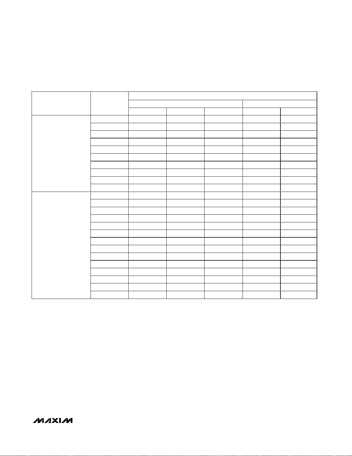
Factory-trimmed voltage thresholds are available in approximately 100mV increments with a 1.5% room temperature variance.
Note: Parts marked with an asterisk (*) are standard versions.
Table 1. Factory-Trimmed Thresholds
PART SUFFIX
MIN TYP MAX MIN MAX
22* 2.167 2.200 2.233 2.145 2.250
23* 2.285 2.320 2.355 2.262 2.375
24 2.364 2.400 2.436 2.340 2.460
MAX6406BS
MAX6407BS
MAX6408BS
MAX6409BS
MAX6410BS
MAX6411BS
25 2.462 2.500 2.537 2.437 2.562
26* 2.591 2.630 2.669 2.564 2.692
27 2.660 2.700 2.741 2.633 2.768
28 2.758 2.800 2.842 2.730 2.870
29* 2.886 2.930 2.974 2.857 3.000
30 2.955 3.000 3.045 2.925 3.075
31* 3.034 3.080 3.126 3.003 3.150
33 3.250 3.300 3.350 3.217 3.383
34 3.349 3.400 3.451 3.315 3.485
35 3.447 3.500 3.552 3.412 3.587
36 3.546 3.600 3.654 3.510 3.690
37 3.644 3.700 3.755 3.607 3.792
38 3.743 3.800 3.857 3.705 3.895
39 3.841 3.900 3.958 3.802 3.997
40 3.940 4.000 4.060 3.900 4.100
41 4.038 4.100 4.161 3.997 4.202
42 4.137 4.200 4.263 4.095 4.305
43 4.235 4.300 4.364 4.192 4.407
44* 4.314 4.380 4.446 4.270 4.489
45 4.432 4.500 4.567 4.387 4.612
46* 4.560 4.630 4.699 4.514 4.746
Threshold Voltage, VTH (V)
TA = +25°CT
= -40°C to +85°C
A

MAX6406–MAX6411
Detailed Description
Manual Reset Input
Many µP-based products require manual reset capability, allowing the operator, a test technician, or external
logic circuit to initiate a reset. A logic low on MR asserts
OUT/OUT. OUT/OUT remains asserted while MR is low.
This input has an internal 50kΩ pullup resistor, so it can
be left open if it is not used. MR can be driven with TTL
or CMOS logic levels, or with open-drain/collector outputs. Connect a normally open momentary switch from
MR to GND to create a manual reset function. If MR is
driven from long cables or if the device is used in a
noisy environment, connect a 0.1µF capacitor from MR
to ground to provide additional noise immunity.
Applications Information
Interfacing to Different Logic
Voltage Components
The MAX6408/MAX6411 have an active-low, opendrain output. This output structure will sink current
when OUT is asserted. Connect a pullup resistor from
OUT to any supply voltage up to 5.5V (Figure 1). Select
a resistor value large enough to allow a valid logic low
(see Electrical Characteristics), and small enough to
register a logic high while supplying all input currents
and leakage paths connected to the OUT line.
Voltage Detectors in 4-Bump (2 X2)
Chip-Scale Package
6 _______________________________________________________________________________________
Table 2. Device Marking Codes
PART TOP MARK PART TOP MARK PART TOP MARK
MAX6406BS31-T AEF
MAX6406BS30-T AEE
MAX6406BS29-T AED
MAX6406BS28-T AEC
MAX6406BS27-T AEB
MAX6406BS26-T AEA
MAX6406BS25-T ADZ
MAX6406BS24-T ADY
MAX6406BS23-T ADX
MAX6406BS22-T ADW
MAX6407BS31-T AEP MAX6408BS31-T AEZ
MAX6407BS30-T AEO MAX6408BS30-T AEY
MAX6407BS29-T AEN MAX6408BS29-T AEX
MAX6407BS28-T AEM MAX6408BS28-T AEW
MAX6407BS27-T AEL MAX6408BS27-T AEV
MAX6407BS26-T AEK MAX6408BS26-T AEU
MAX6407BS25-T AEJ MAX6408BS25-T AET
MAX6407BS24-T AEI MAX6408BS24-T AES
MAX6407BS23-T AEH MAX6408BS23-T AER
MAX6407BS22-T AEG MAX6408BS22-T AEQ
PART TOP MARK
MAX6409BS46-T AFN
MAX6409BS45-T AFM
MAX6409BS44-T AFL
MAX6409BS43-T AFK
MAX6409BS42-T AFJ
MAX6409BS41-T AFI
MAX6409BS40-T AFH
MAX6409BS39-T AFG
MAX6409BS38-T AFF
MAX6409BS37-T AFE
MAX6409BS36-T AFD
MAX6409BS35-T AFC
MAX6409BS34-T AFB
MAX6409BS33-T AFA
MAX6410BS46-T AAX MAX6411BS46-T ABL
MAX6410BS45-T AAW MAX6411BS45-T ABK
MAX6410BS44-T AAV MAX6411BS44-T ABJ
MAX6410BS43-T AAU MAX6411BS43-T ABI
MAX6410BS42-T AAT MAX6411BS42-T ABH
MAX6410BS41-T AAS MAX6411BS41-T ABG
MAX6410BS40-T AAR MAX6411BS40-T ABF
MAX6410BS39-T AAQ MAX6411BS39-T ABE
MAX6410BS38-T AAP MAX6411BS38-T ABD
MAX6410BS37-T AAO MAX6411BS37-T ABC
MAX6410BS36-T AAN MAX6411BS36-T ABB
MAX6410BS35-T AAM MAX6411BS35-T ABA
MAX6410BS34-T AAL MAX6411BS34-T AAZ
MAX6410BS33-T AAK MAX6411BS33-T AAY
PART TOP MARK PART TOP MARK

Negative-Going VCCTransients
These devices are relatively immune to short-duration,
negative-going VCCtransients (glitches).
The Typical Operating Characteristics show the
Maximum Transient Duration vs. Threshold Overdrive
graph, for which output pulses are not generated. The
graph shows the maximum pulse width that a negativegoing VCCtransient may typically have before the
devices issue output signals. As the amplitude of the
transient increases, the maximum allowable pulse width
decreases.
UCSP Reliability
The chip-scale package (UCSP) represents a unique
packaging form factor that may not perform equally to a
packaged product through traditional mechanical reliability tests. CSP reliability is integrally linked to the user’s
assembly methods, circuit board material, and usage
environment. The user should closely review these areas
when considering use of a CSP package. Performance
through Operating Life Test and Moisture Resistance
remains uncompromised as it is primarily determined by
the wafer-fabrication process.
Mechanical stress performance is a greater consideration for a CSP package. CSPs are attached through
direct solder contact to the user’s PC board, foregoing
the inherent stress relief of a packaged product lead
frame. Solder joint contact integrity must be considered.
Information on Maxim’s qualification plan, test data, and
usage recommendations are detailed in the UCSP application note, which can be found on Maxim’s website at
www.maxim-ic.com.
Chip Information
TRANSISTOR COUNT: 512
PROCESS: BiCMOS
MAX6406–MAX6411
Voltage Detectors in 4-Bump (2 X2)
Chip-Scale Package
_______________________________________________________________________________________ 7
Figure 1. Interfacing to Different Logic Voltage Components
Pin Configuration
V
IN
3.6V
Li+
V
CC
MR
(OPEN-DRAIN)
DC/DC
CONVERTER
MAX6408/
MAX6411
GND
V
OUT
OUT
REGULATED 3.0V
SUSPEND
V
CC
µP
TOP VIEW AFTER ASSEMBLED ON PC BOARD (BUMPS AT THE BOTTOM)
45 MIL
UCSP
V
MR
CC
MAX6406MAX6411
45 MIL
OUT (OUT)
( ) ARE FOR MAX6407/MAX6410
GND
A1 A2
B1 B2
MAX6406–MAX6411
Voltage Detectors in 4-Bump (2 X2)
Chip-Scale Package
Maxim cannot assume responsibility for use of any circuitry other than circuitry entirely embodied in a Maxim product. No circuit patent licenses are
implied. Maxim reserves the right to change the circuitry and specifications without notice at any time.
8 _____________________Maxim Integrated Products, 120 San Gabriel Drive, Sunnyvale, CA 94086 408-737-7600
© 2001 Maxim Integrated Products Printed USA is a registered trademark of Maxim Integrated Products.
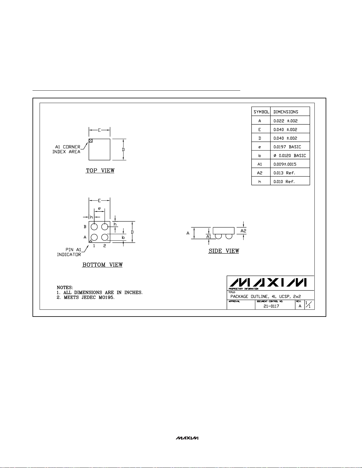
Package Information
Maxim cannot assume responsibility for use of any circuitry other than circuitry entirely embodied in a Maxim product. No circuit patent licenses are
implied. Maxim reserves the right to change the circuitry and specifications without notice at any time.
8 _____________________Maxim Integrated Products, 120 San Gabriel Drive, Sunnyvale, CA 94086 408-737-7600
© 2001 Maxim Integrated Products Printed USA is a registered trademark of Maxim Integrated Products.
4L, UCSP 2x2.EPS
 Loading...