


General Description
The MAX6381–MAX6390 microprocessor (µP) supervisory
circuits monitor power supply voltages from +1.8V to
+5.0V while consuming only 3µA of supply current at
+1.8V. Whenever VCCfalls below the factory-set reset
thresholds, the reset output asserts and remains asserted for a minimum reset timeout period after VCCrises
above the reset threshold. Reset thresholds are available
from +1.58V to +4.63V, in approximately 100mV increments. Seven minimum reset timeout delays ranging
from 1ms to 1200ms are available.
The MAX6381/MAX6384/MAX6387 have a push-pull
active-low reset output. The MAX6382/MAX6385/
MAX6388 have a push-pull active-high reset output,
and the MAX6383/MAX6386/MAX6389/MAX6390
have an open-drain active-low reset output. The
MAX6384/MAX6385/MAX6386 also feature a
debounced manual reset input (with internal pullup
resistor). The MAX6387/MAX6388/MAX6389 have an
auxiliary input for monitoring a second voltage. The
MAX6390 offers a manual reset input with a longer V
CC
reset timeout period (1120ms or 1200ms) and a shorter
manual reset timeout (140ms or 150ms).
The MAX6381/MAX6382/MAX6383 are available in 3-pin
SC70 packages and the MAX6384–MAX6390 are available in 4-pin SC70 packages.
________________________Applications
Computers
Controllers
Intelligent Instruments
Critical µP and µC Power Monitoring
Portable/Battery-Powered Equipment
Dual Voltage Systems
Features
♦ Factory-Set Reset Threshold Voltages Ranging
from +1.58V to +4.63V in Approximately 100mV
Increments
♦ ±2.5% Reset Threshold Accuracy Over
Temperature (-40°C to +125°C)
♦ Seven Reset Timeout Periods Available: 1ms,
20ms, 140ms, 280ms, 560ms, 1120ms,
1200ms (min)
♦ 3 Reset Output Options
Active-Low Push-Pull
Active-High Push-Pull
Active-Low Open-Drain
♦ Reset Output State Guaranteed Valid
Down to V
CC
= 1V
♦ Manual Reset Input (MAX6384/MAX6385/MAX6386)
♦ Auxiliary RESET IN
(MAX6387/MAX6388/MAX6389)
♦ V
CC
Reset Timeout (1120ms or 1200ms)/Manual
Reset Timeout (140ms or 150ms) (MAX6390)
♦ Negative-Going V
CC
Transient Immunity
♦ Low Power Consumption of 6µA at +3.6V
and 3µA at +1.8V
♦ Pin Compatible with
MAX809/MAX810/MAX803/MAX6326/MAX6327/
MAX6328/MAX6346/MAX6347/MAX6348,
and MAX6711/MAX6712/MAX6713
♦ Tiny 3-Pin SC70 and 4-Pin SC70 Packages
MAX6381–MAX6390
SC70, Single/Dual Low-Voltage,
Low-Power µP Reset Circuits
________________________________________________________________ Maxim Integrated Products 1
Pin Configurations
19-1839; Rev 1; 04/01
Ordering Information
Pin Configurations continued at end of data sheet.
Ordering Information continued at end of data sheet.
Typical Operating Circuit appears at end of data sheet.
Selector Guide appears at end of data sheet.
Note: Insert reset threshold suffix (see Reset Threshold table)
after "XR" or "XS". Insert reset timeout delay (see Reset Timeout
Delay table) after "D" to complete the part number. Sample
stock is generally held on standard versions only (see
Standard Versions table). Standard versions have an order
increment requirement of 2500 pieces. Nonstandard versions
have an order increment requirement of 10,000 pieces.
Contact factory for availability of nonstandard versions.
*MAX6390 is available with D4 or D7 timing only.
For pricing, delivery, and ordering information, please contact Maxim/Dallas Direct! at
1-888-629-4642, or visit Maxim’s website at www.maxim-ic.com.
TOP VIEW
PART TEMP. RANGE PIN-PACKAGE
MAX6381XR_ _D_-T -40°C to +125°C 3 SC70-3
MAX6382XR_ _D_-T -40°C to +125°C 3 SC70-3
MAX6383XR_ _D_-T -40°C to +125°C 3 SC70-3
1
GND
MAX6381
MAX6382
RESET
(RESET)
( ) IS FOR MAX6382
MAX6383
2
SC70
3 V
CC
MAX6381–MAX6390
SC70, Single/Dual Low-Voltage,
Low-Power µP Reset Circuits
2 _______________________________________________________________________________________
ABSOLUTE MAXIMUM RATINGS
ELECTRICAL CHARACTERISTICS
(VCC= full range, TA= -40°C to +125°C, unless otherwise specified. Typical values are at TA= +25°C.) (Note 1)
Stresses beyond those listed under “Absolute Maximum Ratings” may cause permanent damage to the device. These are stress ratings only, and functional
operation of the device at these or any other conditions beyond those indicated in the operational sections of the specifications is not implied. Exposure to
absolute maximum rating conditions for extended periods may affect device reliability.
V
CC
to GND ..........................................................-0.3V to +6.0V
RESET Open-Drain Output....................................-0.3V to +6.0V
RESET, RESET (Push-Pull Output) .............-0.3V to (V
CC
+ 0.3V)
MR, RESET IN.............................................-0.3V to (V
CC
+ 0.3V)
Input Current (V
CC
).............................................................20mA
Output Current (All Pins) .....................................................20mA
Continuous Power Dissipation (T
A
= +70°C)
3-Pin SC70 (derate 2.9mW/°C above +70°C)........235mW
4-Pin SC70 (derate 3.1mW/°C above +70°C)........245mW
Operating Temperature Range .........................-40°C to +125°C
Storage Temperature Range .............................-65°C to +150°C
Lead Temperature (soldering, 10s) .................................+300°C
PARAMETER SYMBOL CONDITIONS MIN TYP MAX UNITS
Operating Voltage Range V
CC
VCC = 5.5V, no load 7 13
VCC Supply Current I
CC
VCC = 3.6V, no load 6 11
VCC = 2.5V, no load 4 7
VCC = 1.8V, no load 3 6
V
Reset Threshold
CC
(See Reset Thresholds table)
V
TA = +25°C
TH
TA = -40°C to +125°C
Reset Threshold Tempco ∆VTH/°C 60 ppm/°C
VCC to Reset Delay
falling at 10mV/µs from V
CC
- 100mV
to V
TH
+ 100mV
TH
V
D1 1 2
D2 20 40
Reset Timeout Period
MAX6381–MAX6389
(See Reset Timeout table)
t
RP
D3 140 280
D5 280 560
D6 560 1120
D4 1120 2240
D7 1200 2400
D4 140 280
D7 150 300
D4 1120 2240
D7 1200 2400
Reset Timeout Period
MAX6390
MR timeout period
t
RP
VCC timeout period
V
IL
VTH < 4V
MR Input Voltage
V
IH
V
IL
V
VTH > 4V
IH
1.0 5.5 V
V
TH
1.5%
V
TH
2.5%
V
V
TH
TH
V
TH
1.5%
V
TH
2.5%
+
+
35 µs
✕
0.3
V
CC
✕
0.7
V
CC
0.8
2.4
µA
V
ms
ms
V
MAX6381–MAX6390
SC70, Single/Dual Low-Voltage,
Low-Power µP Reset Circuits
_______________________________________________________________________________________ 3
ELECTRICAL CHARACTERISTICS (continued)
(VCC= full range, TA= -40°C to +125°C, unless otherwise specified. Typical values are at TA= +25°C.) (Note 1)
Note 1: Specifications over temperature are guaranteed by design, not production tested.
PARAMETER SYMBOL CONDITIONS MIN TYP MAX UNITS
MR Minimum Input Pulse Width 1 µs
MR Glitch Rejection 100 ns
MR to Reset Delay 200 ns
MR Internal Pullup Resistance
MAX6381–MAX6389 32 63 100 kΩ
MAX6390 800 1350 2300 Ω
TA = +25°C 1.245 1.27 1.295
Reset IN Input Threshold V
THRST
TA = 0°C to +85°C 1.232 1.308
TA = -40°C to +125°C 1.219 1.321
RESET IN to RESET Delay
RESET IN Input Leakage Current I
Open-Drain RESET Output
Voltage
Open-Drain RESET Output
Leakage Current
Push-Pull RESET Output Voltage
Push-Pull RESET Output Voltage
RESET
V
OL
I
LKG
V
OL
V
OH
V
OH
V
OL
V
V
IN
VCC ≥ 4.5V, I
VCC ≥ 2.5V, I
VCC ≥ 1.0V, I
VCC > VTH, RESET not asserted 1.0 µA
VCC ≥ 4.5V, I
VCC ≥ 2.5V, I
VCC ≥ 1.0V, I
VCC ≥ 4.5V, I
asserted
VCC ≥ 2.5V, I
asserted
VCC ≥ 4.5V, I
VCC ≥ 2.5V, I
VCC ≥ 1.8V, I
VCC ≥ 1.0V, I
VCC ≥ 4.5V, I
asserted
VCC ≥ 2.5V, I
asserted
falling at 4mV/µs from
RESETIN
+ 40mV to V
THRST
SINK
SINK
SINK
SINK
SINK
SINK
SOURCE
SOURCE
SOURCE
SOURCE
SOURCE
SOURCE
SINK
SINK
THRST
- 40mV
4.5 µs
-50 ±1 +50 nA
= 3.2mA, reset asserted 0.4
= 1.2mA, reset asserted 0.3
= 80µA, reset asserted 0.3
= 3.2mA, reset asserted 0.4
= 1.2mA, reset asserted 0.3
= 80µA, reset asserted 0.3
= 800µA, reset not
= 500µA, reset not
= 800µA, reset asserted
= 500µA, reset asserted
= 150µA, reset asserted
= 1µA, reset asserted
= 3.2mA, reset not
= 1.2mA, reset not
0.8
V
0.8
V
0.8
V
0.8
V
0.8
V
0.8
V
✕
CC
✕
CC
✕
CC
✕
CC
✕
CC
✕
CC
0.4
0.3
V
V
V
V
MAX6381–MAX6390
SC70, Single/Dual Low-Voltage,
Low-Power µP Reset Circuits
4 ______________________________________________________________________________________
Typical Operating Characteristics
(TA = +25°C, unless otherwise noted.)
0
2
1
5
4
3
6
7
8
9
-40 -10 5-25 20 35 50 65 80 95 110 125
SUPPLY CURRENT vs. TEMPERATURE
(NO LOAD)
MAX6381/90 toc01
TEMPERATURE (°C)
SUPPLY CURRENT (µA)
VCC = +5.5V
VCC = +3.6V
VCC = +1.8V
V
CC
= +2.5V
25
29
27
35
33
31
37
39
41
43
-40 -10 5-25 20 35 50 65 80 95 110 125
POWER-DOWN RESET DELAY
vs. TEMPERATURE
MAX6381/90 toc02
TEMPERATURE (°C)
POWER-DOWN RESET DELAY (µs)
VCC = +3.0V
VCC = +1.8V
0.94
0.98
0.96
1.02
1.00
1.06
1.04
1.08
-40 -10 5 20-25 35 50 65 80 95 110 125
NORMALIZED POWER-UP RESET TIMEOUT
vs. TEMPERATURE
MAX6381/90 toc03
TEMPERATURE (°C)
NORMALIZED RESET TIMEOUT PERIOD
0.990
0.985
1.015
0.995
0.990
1.000
1.005
1.010
1.020
-40 -10 5 20-25 35 50 9580 11065 125
MAX6381/90 toc04
TEMPERATURE (°C)
NORMALIZED RESET THRESHOLD
NORMALIZED RESET THRESHOLD
vs. TEMPERATURE
0
0.4
0.2
0.8
0.6
1.0
1.2
063912
OUTPUT VOLTAGE LOW
vs. SINK CURRENT
MAX6381/90 toc05
I
SINK
(mA)
V
OL
(V)
VCC = +3.0V
VCC = +4.5V
0
1.0
0.5
2.0
1.5
2.5
3.0
0 500 750250 1000 1250 1500
OUTPUT VOLTAGE HIGH
vs. SOURCE CURRENT
MAX6381/90 toc06
I
SOURCE
(µA)
V
OH
(V)
VCC = +2.5V
VCC = +1.8V
450
0
1 100010010
MAXIMUM TRANSIENT DURATION
vs. RESET COMPARATOR OVERDRIVE
150
50
350
250
500
200
100
400
300
MAX6381/90 toc07
RESET COMPARATOR OVERDRIVE, VTH - VCC (mV)
MAXIMUM TRANSIENT DURATION (µs)
RESET ASSERTED
ABOVE THIS LINE
3.5
3.9
3.7
4.5
4.3
4.1
4.7
4.9
5.3
5.1
5.5
-40 -10 5-25 20 35 50 65 80 95 110 125
RESET IN TO RESET DELAY
vs. TEMPERATURE
MAX6381/90 toc08
TEMPERATURE (°C)
RESET IN DELAY (µs)

MAX6381–MAX6390
SC70, Single/Dual Low-Voltage,
Low-Power µP Reset Circuits
_______________________________________________________________________________________ 5
Pin Description
PIN
MAX6381/
MAX6383
— 2 — 2 — 2 RESET
—— 33——MR
———— 33
MAX6382
1 1 1 1 1 1 GND Ground
2 — 2 — 2 — RESET
334444V
MAX6384/
MAX6386/
MAX6390
MAX6385
MAX6387/
MAX6389
MAX6388
NAME FUNCTION
RESET
IN
CC
Active-High Push-Pull Reset Output. RESET
changes from low to high when any
monitored voltage (V
below the reset threshold or MR is pulled low.
RESET remains high for the reset timeout
period after monitored voltages exceed the
reset thresholds or MR is released.
Active-Low Open-Drain/Push-Pull Reset
Output. RESET changes from high to low when
any monitored voltage (V
drops below the reset threshold or MR is
pulled low.
timeout period after the monitored voltages
exceed the reset thresholds or MR is released.
Open-drain requires an external pullup
resistor.
Active-Low Manual Reset Input. Drive low to
force a reset. Reset remains active as long
as MR is low and for the reset timeout period
after MR is released. Leave unconnected or
connect to V
63kΩ (1.35kΩ for MAX6390) pullup resistor to
V
CC
Auxiliary Reset Input. High-impedance input
to the auxiliary reset comparator. Connect
RESET IN to the center point of an external
resistor voltage-divider network to set the
reset threshold voltage. Reset asserts when
either V
threshold voltage.
Supply Voltage for the device and input for
fixed V
RESET
if unused. MR has an internal
CC
.
or RESET IN falls below its
CC
reset threshold monitor.
CC
or V
CC
or V
CC
remains low for the reset
RESETIN
RESETIN
) drops
)

MAX6381–MAX6390
SC70, Single/Dual Low-Voltage,
Low-Power µP Reset Circuits
6 _______________________________________________________________________________________
Detailed Description
RESET Output
A µP reset input starts the µP in a known state. These
µP supervisory circuits assert reset to prevent code
execution errors during power-up, power-down, or
brownout conditions.
Reset asserts when VCCis below the reset threshold;
once VCCexceeds the reset threshold, an internal timer
keeps the reset output asserted for the reset timeout
period. After this interval, reset output deasserts. Reset
output is guaranteed to be in the correct logic state for
VCC≥ 1V.
Manual Reset Input (MAX6384/
MAX6385/MAX6386/MAX6390)
Many µP-based products require manual reset capability, allowing the operator, a test technician, or external
logic circuitry to initiate a reset. A logic low on MR
asserts reset. Reset remains asserted while MR is low,
and for the reset active timeout period (tRP) after MR
returns high. This input has an internal 63kΩ pullup
resistor (1.35kΩ for MAX6390), so it can be left unconnected if it is not used. MR can be driven with TTL or
CMOS logic levels, or with open-drain/collector outputs.
Connect a normally open momentary switch from MR to
GND to create a manual-reset function; external
debounce circuitry is not required. If MR is driven from
long cables or if the device is used in a noisy environment, connecting a 0.1µF capacitor from MR to GND
provides additional noise immunity.
RESET IN Comparator
(MAX6387/MAX6388/MAX6389)
RESET IN is compared to an internal +1.27V reference.
If the voltage at RESET IN is less than 1.27V, reset
asserts. Use the RESET IN comparator as a useradjustable reset detector or as a secondary power-supply monitor by implementing a resistor-divider at RESET
IN (shown in Figure 1). Reset asserts when either V
CC
or RESET IN falls below its respective threshold voltage. Use the following equation to set the threshold:
V
INTH
= V
THRST
(R1/R2 + 1)
where V
THRST
= +1.27V. To simplify the resistor selec-
tion, choose a value of R2 and calculate R1:
R1 = R2 [(V
INTH/VTHRST
) - 1]
Since the input current at RESET IN is 50nA (max),
large values can be used for R2 with no significant loss
in accuracy.
___________Applications Information
Negative-Going VCCTransients
In addition to issuing a reset to the µP during power-up,
power-down, and brownout conditions, the
MAX6381–MAX6390 are relatively immune to short duration negative-going VCCtransients (glitches).
The Typical Operating Characteristics section shows the
Maximum Transient Durations vs. Reset Comparator
Overdrive, for which the MAX6381–MAX6390 do not
generate a reset pulse. This graph was generated using
Reset Thresholds (-40°C to +125°C)
SUFFIX VTH (min) VTH (nom) VTH (max)
46 4.51 4.63 4.74
45 4.39 4.50 4.61
44 4.27 4.38 4.48
43 4.19 4.30 4.41
42 4.10 4.20 4.31
41 4.00 4.10 4.20
40 3.90 4.00 4.10
39 3.80 3.90 4.00
38 3.71 3.80 3.90
37 3.61 3.70 3.79
36 3.51 3.60 3.69
35 3.41 3.50 3.59
34 3.32 3.40 3.49
33 3.22 3.30 3.38
32 3.12 3.20 3.28
31 3.00 3.08 3.15
30 2.93 3.00 3.08
29 2.85 2.93 3.00
28 2.73 2.80 2.87
27 2.63 2.70 2.77
26 2.56 2.63 2.69
25 2.44 2.50 2.56
24 2.34 2.40 2.46
23 2.26 2.31 2.37
22 2.13 2.19 2.24
21 2.05 2.10 2.15
20 1.95 2.00 2.05
19 1.85 1.90 1.95
18 1.76 1.80 1.85
17 1.62 1.67 1.71
16 1.54 1.58 1.61

a negative-going pulse applied to VCC, starting above the
actual reset threshold and ending below it by the magnitude indicated (reset comparator overdrive). The graph
indicates the typical maximum pulse width a negativegoing V
CC
transient may have without causing a reset
pulse to be issued. As the magnitude of the transient
increases (goes farther below the reset threshold), the
maximum allowable pulse width decreases. A 0.1µF
capacitor mounted as close as possible to VCCprovides
additional transient immunity.
Ensuring a Valid RESET
Output Down to V
CC
= 0
The MAX6381–MAX6390 are guaranteed to operate
properly down to VCC= 1V. In applications that require
valid reset levels down to VCC= 0, a pulldown resistor to
active-low outputs (push/pull only, Figure 2) and a
pullup resistor to active-high outputs (push/pull only) will
ensure that the reset line is valid while the reset output
can no longer sink or source current. This scheme does
not work with the open-drain outputs of the
MAX6383/MAX6386/MAX6389/MAX6390. The resistor
value used is not critical, but it must be small enough
not to load the reset output when V
CC
is above the reset
threshold. For most applications, 100kΩ is adequate.
MAX6381–MAX6390
SC70, Single/Dual Low-Voltage,
Low-Power µP Reset Circuits
_______________________________________________________________________________________ 7
Figure 1. RESET IN Configuration
Figure 2. RESET Valid to V
CC
= Ground Circuit
Standard Versions
Reset Timeout Delay
* The MAX6390 has a 1120ms or 1200ms
RESET
timeout and a
140ms or 150ms manual reset timeout
V
CC
V
IN
R1
R2
SUFFIX MIN
D1 1ms
D2 20ms
D3 140ms
D5 280ms
D6 560ms
D4 1120ms
D7 1200ms
MAX6390XSD4 1120/140ms *
MAX6390XSD7 1200/150ms *
MAX6387
MAX6388
MAX6389
RESET IN
RESET
(RESET)
GND
( ) IS FOR MAX6388
V
CC
MAX6381
MAX6384
MAX6387
RESET
R1
100k
GND
PART
MAX638_
MAX6390
RESET
THRESHOLD
46
44
31
29
26
23
22
17
16
46
44
31
29
26
23
22
17
16
RESET TIMEOUT
D3
D4
MAX6381–MAX6390
SC70, Single/Dual Low-Voltage,
Low-Power µP Reset Circuits
8 _______________________________________________________________________________________
Selector Guide
*The MAX6390 offers a VCCreset timeout of 1120ms or 1200ms (min) and a manual reset timeout of 140ms or 150ms (min).
Chip Information
TRANSISTOR COUNT: 647
PROCESS: BiCMOS
*MRis for MAX6384/MAX6385/MAX6386/MAX6390
** RESET IN is for MAX6387/MAX6388/MAX6389
( ) are for MAX6382/MAX6385/MAX6388
( ) IS FOR MAX6388
SC70
TOP VIEW
1
2
4
3
V
CC
RESET
(RESET)
GND
MAX6387
MAX6388
MAX6389
1
2
4
3
V
CC
MR
RESET
(RESET)
GND
MAX6384
MAX6385
MAX6386
MAX6390
( ) IS FOR MAX6385
SC70
RESET IN
Pin Configurations (continued)
Typical Operating Circuit
PART NUMBER
PUSH-PULL
ACTIVE-LOW
PUSH-PULL
ACTIVE-HIGH
OPEN-DRAIN
ACTIVE-LOW
MANUAL RESET
INPUT MR
MAX6381 X
MAX6382 X
MAX6383 X
MAX6384 X X
MAX6385 X X
MAX6386 X X
MAX6390* X X
MAX6387 X X
MAX6388 X X
MAX6389 X X
V
CORE
R1
R1
PUSHBUTTON SWITCH
I/O SUPPLY
V
CC
RESET IN **
MR *
MAX6381–MAX6390
(RESET)
GND
RESET
CORE
VOLTAGE
RESET
INPUT
I/O
VOLTAGE
µP
GND
RESET IN
MAX6381–MAX6390
SC70, Single/Dual Low-Voltage,
Low-Power µP Reset Circuits
_______________________________________________________________________________________ 9
Ordering Information
(continued)
Note: Insert reset threshold suffix (see Reset Threshold table)
after "XR" or "XS". Insert reset timeout delay (see Reset Timeout
Delay table) after "D" to complete the part number. Sample
stock is generally held on standard versions only (see
Standard Versions table). Standard versions have an order
increment requirement of 2500 pieces. Nonstandard versions
have an order increment requirement of 10,000 pieces.
Contact factory for availability of nonstandard versions.
*MAX6390 is available with D4 or D7 timing only.
PART TEMP. RANGE PIN-PACKAGE
MAX6384XS_ _D_-T -40°C to +125°C 4 SC70-4
MAX6385XS_ _D_-T -40°C to +125°C 4 SC70-4
MAX6386XS_ _D_-T -40°C to +125°C 4 SC70-4
MAX6387XS_ _D_-T -40°C to +125°C 4 SC70-4
MAX6388XS_ _D_-T -40°C to +125°C 4 SC70-4
MAX6389XS_ _D_-T -40°C to +125°C 4 SC70-4
MAX6390XS_ _D_-T* -40°C to +125°C 4 SC70-4
MAX6381–MAX6390
SC70, Single/Dual Low-Voltage,
Low-Power µP Reset Circuits
10 ______________________________________________________________________________________
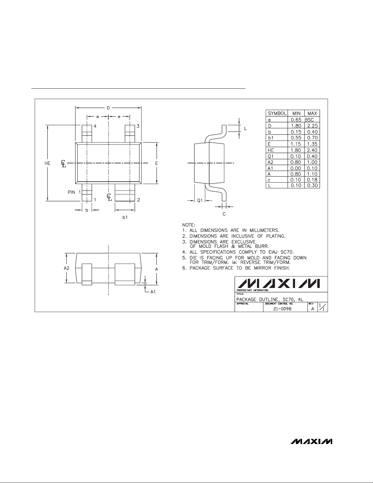
Package Information
SC70, 4L.EPS

SC70, Single/Dual Low-Voltage,
Low-Power µP Reset Circuits
Maxim cannot assume responsibility for use of any circuitry other than circuitry entirely embodied in a Maxim product. No circuit patent licenses are
implied. Maxim reserves the right to change the circuitry and specifications without notice at any time.
Maxim Integrated Products, 120 San Gabriel Drive, Sunnyvale, CA 94086 408-737-7600 ____________________ 11
© 2001 Maxim Integrated Products Printed USA is a registered trademark of Maxim Integrated Products.
MAX6381–MAX6390
Package Information (continued)
SC70, 3L.EPS
 Loading...