

General Description
The MAX6365–MAX6368 supervisory circuits simplify
power-supply monitoring, battery-backup control functions, and memory write protection in microprocessor
(µP) systems. The circuits significantly improve the size,
accuracy, and reliability of modern systems with an ultrasmall integrated solution.
These devices perform four basic system functions:
1) Provide a µP reset output during VCCsupply powerup, power-down, and brownout conditions.
2) Internally control VCCto backup-battery switching to
maintain data or low-power operation for CMOS
RAM, CMOS µPs, real-time clocks, and other digital
logic when the main supply fails.
3) Provide memory write protection through internal
chip-enable gating during supply or processor faults.
4) Include one of the following options: a manual reset
input (MAX6365), a watchdog timer function
(MAX6366), a battery-on output (MAX6367), or an
auxiliary user-adjustable reset input (MAX6368).
The MAX6365–MAX6368 operate from VCCsupply voltages as low as 1.2V. The factory preset reset threshold
voltages range from 2.32V to 4.63V (see Ordering
Information). In addition, each part is offered in three
reset output versions: push-pull active low, open-drain
active low, or open-drain active high (see Selector
Guide). The MAX6365–MAX6368 are available in miniature 8-pin SOT23 packages.
Applications
Critical µP/µC Power Portable/BatteryMonitoring Powered Equipment
Fax Machines Set-Top Boxes
Industrial Control POS Equipment
Computers/Controllers
Features
♦ Low +1.2V Operating Supply Voltage (VCCor V
BATT
)
♦ Precision Monitoring of +5.0V, +3.3V, +3.0V, and
+2.5V Power-Supply Voltages
♦ On-Board Gating of Chip-Enable Signals, 1.5ns
Propagation Delay
♦ Debounced Manual Reset Input (MAX6365)
♦ Watchdog Timer, 1.6s Timeout (MAX6366)
♦ Battery-On Output Indicator (MAX6367)
♦ Auxiliary User-Adjustable RESET IN (MAX6368)
♦ Low 10µA Quiescent Supply Current
♦ Three Available Output Structures
Push-Pull RESET
Open-Drain RESET
Open-Drain RESET
♦ RESET/RESET Valid Down to 1.2V Guaranteed
(V
CC
or V
BATT
)
♦ Power-Supply Transient Immunity
♦ 150ms min Reset Timeout Period
♦ Miniature 8-Pin SOT23 Package
MAX6365–MAX6368
SOT23, Low-Power µP Supervisory Circuits
with Battery Backup and Chip-Enable Gating
________________________________________________________________ Maxim Integrated Products 1
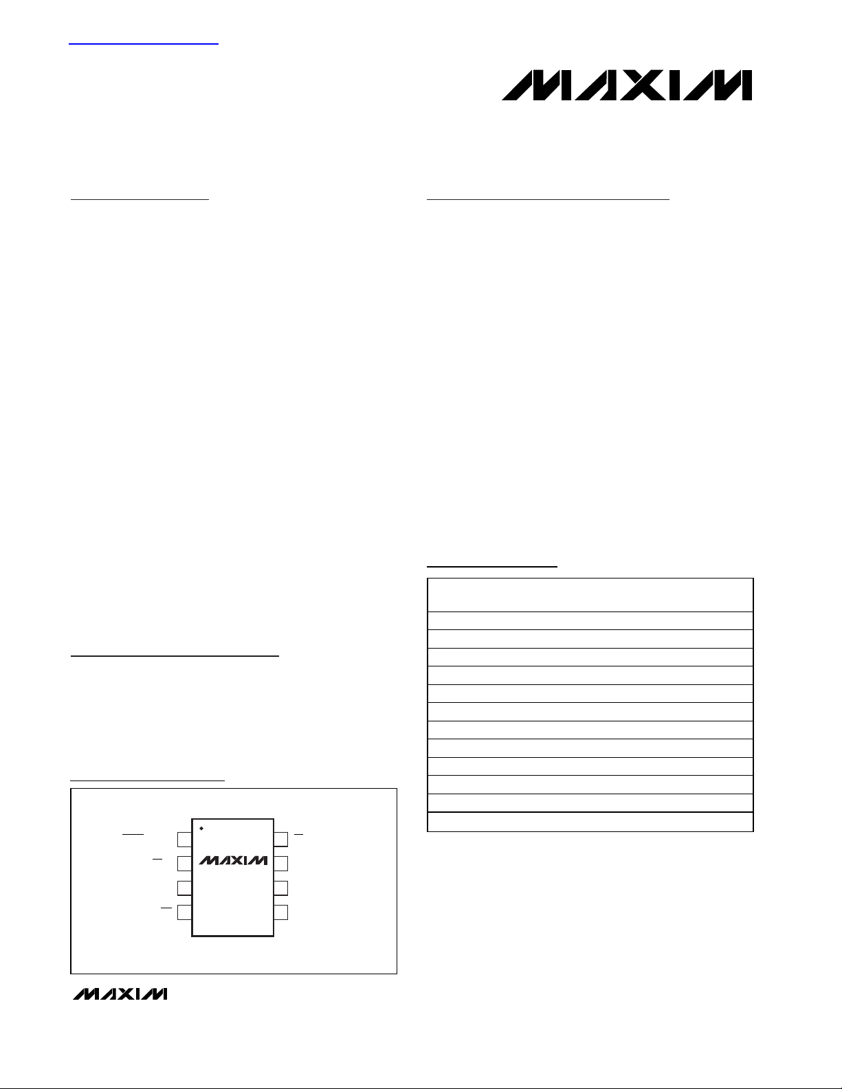
Pin Configurations
19-1658; Rev 1; 6/01
For pricing, delivery, and ordering information, please contact Maxim/Dallas Direct! at
1-888-629-4642, or visit Maxim’s website at www.maxim-ic.com.
Ordering Information
*These parts offer a choice of reset threshold voltages. From the
Reset Threshold Ranges table, insert the desired threshold voltage code in the blank to complete the part number. SOT parts
come in tape-and-reel only and must be ordered in 2500-piece
increments. See Device Marking Codes for a complete parts list,
including SOT top marks and standard threshold versions. See
Selector Guide for a listing of device features.
Pin Configurations continued at end of data sheet.
Typical Operating Circuit appears at end of data sheet.
PART* TEMP. RANGE
PINPACKAGE
-40°C to +85°C 8 SOT23-8
MAX6365PKA_ _-T -40°C to +85°C 8 SOT23-8
-40°C to +85°C 8 SOT23-8
-40°C to +85°C 8 SOT23-8
M A X 6 36 6P K A_ _-T
-40°C to +85°C 8 SOT23-8
M A X 6 36 6H K A_ _-T
-40°C to +85°C 8 SOT23-8
-40°C to +85°C 8 SOT23-8
-40°C to +85°C 8 SOT23-8
-40°C to +85°C 8 SOT23-8
-40°C to +85°C 8 SOT23-8
-40°C to +85°C 8 SOT23-8
-40°C to +85°C 8 SOT23-8
查询MAX6365供应商
TOP VIEW
RESET, RESET
1
2
GND
3
4
MR
87CE OUT
MAX6365
SOT23
6
5
BATTCE IN
OUT
V
M A X6 3 6 5 LK A_ _-T
MAX6365HKA_ _-T
M A X6 3 6 6 LK A_ _-T
M A X6 3 6 7 LK A_ _-T
M A X 6 36 7P K A_ _-T
M A X 6 36 7H K A_ _-T
M A X6 3 6 8 LK A_ _-T
M A X 6 36 8P K A_ _-T
M A X 6 36 8H K A_ _-T
CC
MAX6365–MAX6368
SOT23, Low-Power µP Supervisory Circuits
with Battery Backup and Chip-Enable Gating
2 _______________________________________________________________________________________
ABSOLUTE MAXIMUM RATINGS
ELECTRICAL CHARACTERISTICS
(VCC= +2.4V to +5.5V, V
BATT
= +3.0V, CE IN = VCC, reset not asserted, TA= -40°C to +85°C. Typical values are at TA= +25°C,
unless otherwise noted.) (Note 1)
Stresses beyond those listed under “Absolute Maximum Ratings” may cause permanent damage to the device. These are stress ratings only, and functional
operation of the device at these or any other conditions beyond those indicated in the operational sections of the specifications is not implied. Exposure to
absolute maximum rating conditions for extended periods may affect device reliability.
Terminal Voltages (with respect to GND)
V
CC
, BATT, OUT.......................................................-0.3V to +6V
RESET (open drain), RESET (open drain) ................-0.3V to +6V
BATT ON, RESET (push-pull), RESET IN,
WDI, CE IN, CE OUT ...........................-0.3V to (V
OUT
+ 0.3V)
MR ..............................................................-0.3V to (V
CC
+ 0.3V)
Input Current
V
CC
Peak ..............................................................................1A
V
CC
Continuous .............................................................250mA
BATT Peak .....................................................................250mA
BATT Continuous .............................................................40mA
GND ...............................................................................75mA
Output Current
OUT ...............................Short-Circuit Protected for up to 10s
RESET, RESET, BATT ON, CE OUT...............................20mA
Continuous Power Dissipation (T
A
= +70°C)
8-Pin SOT23 (derate 8.75mW/°C above +70°C)........700mW
Operating Temperature Range ...........................-40°C to +85°C
Storage Temperature Range .............................-65°C to +150°C
Junction Temperature .....................................................+150°C
Lead Temperature (soldering, 10s) .................................+300°C
PARAMETER
CONDITIONS
UNITS
Operating Voltage Range
(Note 2)
No load 0 5.5 V
VCC = 2.8V 10 30
VCC = 3.6V 12 35
Supply Current
(Excluding I
OUT
)
I
CC
VCC = 5.5V 15 50
µA
T
A
= +25°C1
Supply Current in Battery-
Backup Mode (Excluding I
OUT
)
I
BACK
V
BATT
= 2.8V,
V
CC
= 0
T
A
= -40°C to +85°C3
µA
T
A
= +25°C
BATT Standby Current I
BATT
+ 0.2V)
T
A
= -40°C to +85°C
µA
VCC = 4.75V, I
OUT
= 150mA 3.1
VCC = 3.15V, I
OUT
= 65mA 3.7VCC to OUT On-Resistance R
ON
VCC = 2.38V, I
OUT
= 25mA 4.6
Ω
V
BATT
= 4.5V, I
OUT
= 20mA
V
BATT
-
V
BATT
= 3.0V, I
OUT
= 10mA
V
BATT
-
Output Voltage in BatteryBackup Mode
V
OUT
V
BATT
= 2.25V, I
OUT
= 5mA
V
BATT
-
V
Power-up 20
Battery-Switchover Threshold
(VCC - V
BATT
)
V
SW
VCC < V
TH
Power-down -20
mV
MAX636_ _KA46
MAX636_ _KA44
MAX636_ _KA31
MAX636_ _KA29
MAX636_ _KA26
Reset Threshold V
TH
MAX636_ _KA23
V
VCC Falling Reset Delay t
RD
V
CC
falling at 10V /ms 20 µs
SYMBOL
MIN TYP MAX
VCC, V
BATT
No load, VCC > V
TH
5.5V > VCC > (V
BATT
-0.1 0.02
-1.0 0.02
0.2
0.15
0.15
4.50 4.63 4.75
4.25 4.38 4.50
3.00 3.08 3.15
2.85 2.93 3.00
2.55 2.63 2.70
2.25 2.32 2.38
MAX6365–MAX6368
SOT23, Low-Power µP Supervisory Circuits
with Battery Backup and Chip-Enable Gating
_______________________________________________________________________________________ 3
ELECTRICAL CHARACTERISTICS (continued)
(VCC= +2.4V to +5.5V, V
BATT
= +3.0V, CE IN = VCC, reset not asserted, TA= -40°C to +85°C. Typical values are at TA= +25°C,
unless otherwise noted.) (Note 1)
PARAMETER SYMBOL CONDITIONS MIN TYP MAX UNITS
Reset Active Timeout Period t
RESET Output Voltage
RESET Output Voltage
RESET Outp ut Leakag e C ur r ent I
RP
V
OL
V
OH
V
OL
Reset asserted,
= 0
V
BATT
Reset not asserted
(MAX636_L only)
Reset not asserted
Reset not asserted,
V
= 0
V
OH
BATT
(MAX636_H only)
(Note 3)
LKG
MAX636_P and MAX636_H only 1 µA
I
= 1.6mA,
SINK
> 2.1V
V
CC
I
= 100µA,
SINK
> 1.2V
V
CC
I
SOURCE
V
> V
CC
I
= 1.6mA,
SINK
V
> V
CC
I
SOURCE
V
> 1.8V
CC
I
SOURCE
> 1.2V
V
CC
= 500µA,
TH(MAX)
TH (MAX)
= 1mA,
= 200µA,
150 280 ms
0.3
0.4
✕
0.8
V
CC
0.3
✕
0.7
V
CC
✕
0.8
V
CC
V
V
MANUAL RESET (MAX6365 only)
✕
0.3
V
CC
V
MR Input Voltage
V
IL
✕
V
IH
0.7
V
CC
Pullup Resistance 20 kΩ
Minimum Pulse Width 1µs
Glitch Immunity VCC = 3.3V 100 ns
MR to Reset Delay VCC = 3.3V 120 ns
WATCHDOG (MAX6366 only)
Watchdog Timeout Period t
Minimum WDI Input Pulse Width t
WDI Input Voltage
WD
WDI
V
V
IH
IL
1.00 1.65 2.25 s
100 ns
✕
0.3
V
CC
✕
0.7
V
CC
V
WDI Input Current -1.0 1.0 µA
BATT ON (MAX6367 only)
Output Voltage V
OL
I
SINK
= 3.2mA, V
= 2.1V 0.4 V
BATT
Sink current, VCC = 5V 60 mA
Output Short-Circuit Current
Source current, V
> 2V 10 30 100 µA
BATT
MAX6365–MAX6368
SOT23, Low-Power µP Supervisory Circuits
with Battery Backup and Chip-Enable Gating
4 _______________________________________________________________________________________
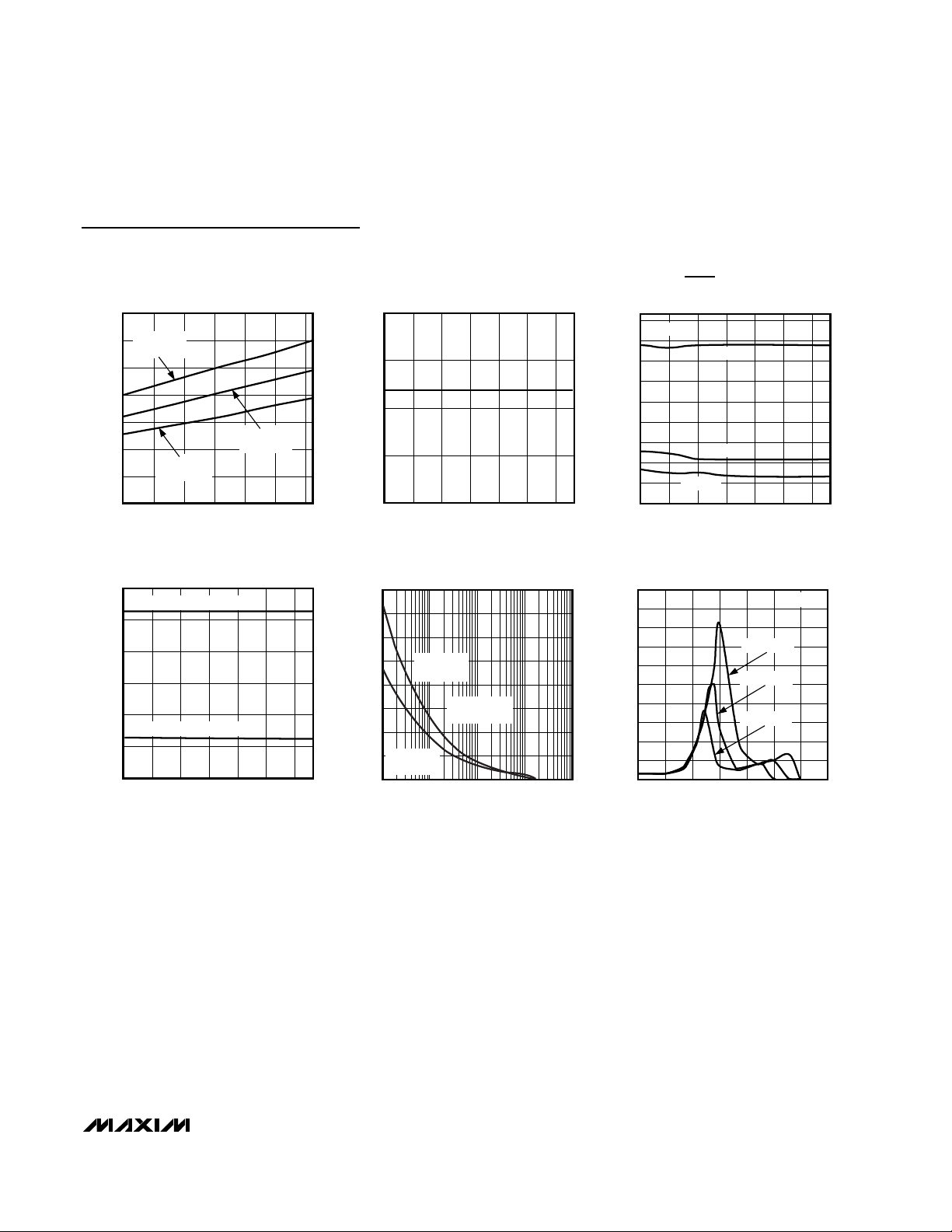
Typical Operating Characteristics
(TA = +25°C, unless otherwise noted.)
8
10
9
12
11
15
14
13
16
-40 0-20 20 40 60 80
SUPPLY CURRENT
vs. TEMPERATURE (NO LOAD)
MAX6365/8-01
TEMPERATURE (°C)
SUPPLY CURRENT (µA)
VCC = 5.0V
V
BATT
= 0
0
0.2
0.6
0.4
0.8
1.0
1.2
BATTERY SUPPLY CURRENT
(BACKUP MODE) vs. TEMPERATURE
MAX6365/8-02
TEMPERATURE (°C)
BATTERY SUPPLY CURRENT (µA)
-40 20 40-20 0 60 80
V
BATT
= 2.0V
VCC = 0
V
BATT
= 2.8V
0
2
1
4
3
7
6
5
8
-40 0-20 20 40 60 80
BATT-TO-OUT ON-RESISTANCE
vs. TEMPERATURE
MAX6365/8-03
TEMPERATURE (°C)
BATT-TO-OUT ON-RESISTANCE (Ω)
V
BATT
= 5.0V
V
BATT
= 2.0V
V
BATT
= 2.8V
I
OUT
= 25mA
V
CC
= 0
ELECTRICAL CHARACTERISTICS (continued)
(VCC= +2.4V to +5.5V, V
BATT
= +3.0V, CE IN = VCC, reset not asserted, TA= -40°C to +85°C. Typical values are at TA= +25°C,
unless otherwise noted.) (Note 1)
PARAMETER
SYMBOL
CONDITIONS
MIN
TYP
MAX
UNITS
RESET IN (MAX6368 only)
RESET IN Threshold V
RTH
V
RESET IN Leakage Current
nA
RESET IN to Reset Delay VOD = 50mV, RESET IN falling 1.5 µs
CHIP-ENABLE GATING
CE IN Leakage Current Reset asserted
µA
CE IN to CE OUT Resistance
Reset not asserted (Note 4) 20
Ω
CE OUT Short-Circuit Current Reset asserted, CE OUT = 0
mA
VCC = 4.75V 1.5 7
CE IN to CE OUT Propagation
Delay
50Ω source,
C
LOAD
= 50pF
V
CC
= 3.15V 2 9
ns
VCC = 5V, VCC
>
V
BATT
, I
SOURCE
= 100µA
CE OUT Output Voltage High
V
CC
= 0, V
BATT
>
2.2V, I
SOURCE
= 1µA
V
BATT
-
0.1
V
Reset-to-CE OUT Delay 12 µs
Note 1: All devices are 100% production tested at TA= +25°C. Limits over temperature are guaranteed by design.
Note 2: V
BATT
can be 0 anytime, or VCCcan go down to 0 if V
BATT
is active (except at startup).
Note 3: RESET is pulled up to OUT. Specifications apply for OUT = V
CC
or OUT = BATT.
Note 4: The chip-enable resistance is tested with V
CC
= V
TH(MAX)
and CE IN = VCC/2.
1.185 1.235 1.285
±0.01 ±25
0.75 2.0
0.8 ✕ V
CC
±1
100
MAX6365–MAX6368
SOT23, Low-Power µP Supervisory Circuits
with Battery Backup and Chip-Enable Gating
_______________________________________________________________________________________ 5
Typical Operating Characteristics (continued)
(TA = +25°C, unless otherwise noted.)
0
0.4
0.2
0.8
0.6
1.2
1.0
1.4
-40 0 20-20 40 60 80
VCC TO OUT ON-RESISTANCE
vs. TEMPERATURE
MAX6365/8-04
TEMPERATURE (°C)
V
CC
TO OUT ON-RESISTANCE (Ω)
VCC = 3.0V
I
OUT
= 65mA
VCC = 4.5V
I
OUT
= 150mA
VCC = 2.3V
I
OUT
= 25mA
190
195
205
200
210
RESET TIMEOUT PERIOD
vs. TEMPERATURE
MAX6365/8-05
TEMPERATURE (°C)
RESET TIMEOUT PERIOD (ms)
-40 20 40-20 0 60 80
0
30
15
75
60
45
135
120
105
90
MAX6365/8-06
TEMPERATURE (°C)
PROPAGATION DELAY (µs)
-40 20 40-20 0 60 80
VCC TO RESET PROPAGATION DELAY
vs. TEMPERATURE
VCC FALLING
0.25V/ms
1V/ms
10V/ms
2.0
3.0
2.5
5.0
4.5
4.0
3.5
RESET THRESHOLD
vs. TEMPERATURE
MAX6365/8-07
TEMPERATURE (°C)
THRESHOLD (V)
-40 20 40-20 0 60 80
MAX636_ 46 (VTH = 4.63V)
MAX636_ 26 (VTH = 2.63V)
1 10010 1000 10,000
MAXIMUM TRANSIENT DURATION
vs. RESET THRESHOLD OVERDRIVE
MAX6365/8-08
RESET THRESHOLD OVERDRIVE V
TH
- VCC (mV)
MAXIMUM TRANSIENT DURATION (µs)
400
300
350
250
200
0
50
150
100
MAX636_ 26
(V
TH
= 2.63V)
MAX636_ 46
(V
TH
= 4.63V)
RESET OCCURS
ABOVE CURVE
0
3
2
1
5
4
9
8
7
6
10
0 0.5 1.0 1.5 2.0 2.5 3.0 3.5
BATTERY SUPPLY CURRENT
vs. SUPPLY VOLTAGE
MAX6365/8-09
VCC (V)
BATTERY SUPPLY CURRENT (µA)
VTH = 2.93V
V
BATT
= 2.8V
V
BATT
= 2.5V
V
BATT
= 2.3V

MAX6365–MAX6368
SOT23, Low-Power µP Supervisory Circuits
with Battery Backup and Chip-Enable Gating
6 _______________________________________________________________________________________
Typical Operating Characteristics (continued)
(TA = +25°C, unless otherwise noted.)
MAX6368
vs. TEMPERATURE
CHIP-ENABLE PROPAGATION DELAY
5
CE IN = 0 TO V
MAX6365/8-11
DRIVER SOURCE
IMPEDANCE = 50Ω
4
3
2
PROPAGATION DELAY (ns)
1
vs. CE OUT LOAD CAPACITANCE
CC
VCC = 3V
VCC = 5V
1.236
(V)
1.235
RTH
V
MAX6368
RESET IN THRESHOLD
vs. TEMPERATURE
MAX6365/8 -10
RESET IN TO RESET PROPAGATION DELAY
V
= 50mV
OD
2.8
2.5
2.2
1.9
1.6
PROPAGATION DELAY (µs)
1.3
MAX6365/8-12
1.234
-40 20 40-20 0 60 80
TEMPERATURE (°C)
1.0
CE IN TO CE OUT ON-RESISTANCE
vs. TEMPERATURE
25
20
VCC = 3.0V
15
10
VCC = 5.0V
5
CE IN TO CE OUT ON-RESISTANCE (Ω)
V
= VCC/2
CE IN
= 0
V
BATT
0
-40 0-20 20 40 60 80
TEMPERATURE (°C)
-40 20 40-20 0 60 80
TEMPERATURE (°C)
2.0
MAX6365/8-13
1.9
1.8
1.7
1.6
1.5
1.4
1.3
1.2
WATCHDOG TIMEOUT PERIOD (s)
1.1
1.0
-40 -20 0 20 40 60 80
0
0 10050 150 200
MAX6366
WATCHDOG TIMEOUT PERIOD
vs. TEMPERATURE
VCC = 5.0V
V
BATT
TEMPERATURE (°C)
= 0
C
(pF)
LOAD
MAX6365/8-14

MAX6365–MAX6368
SOT23, Low-Power µP Supervisory Circuits
with Battery Backup and Chip-Enable Gating
_______________________________________________________________________________________ 7
Pin Description
PIN NAME FUNCTION
RESET
Acti ve- H i g h Reset Outp ut. RE S E T asser ts hi g h conti nuousl y w hen V
C C
i s b el ow the r eset thr eshol d ( V
TH
) ,
MR i s l ow , or RE S E T IN i s l ow . It asser ts i n p ul ses w hen the inter nal w atchd og ti m es out. RE S E T r em ai ns
asser ted for the r eset ti m eout p er i od ( t
RP
) after V
C C
r i ses ab ove the r eset thr eshol d , after the m anual r eset
i np ut g oes fr om l ow to hi g h, after RE S E T IN g oes hi g h, or after the w atchd og tr i g g ers a r eset event.
RE S E T i s an op en- d r ai n acti ve- hi g h r eset outp ut.
1
RESET
Active-Low Reset Output. RESET asserts low continuously when V
C C
is below the reset threshold
(V
TH
), the manual reset input is low, or RESET IN is low. It asserts low in pulses when the internal
watchdog times out. RESET remains asserted low for the reset timeout period (t
RP
) after V
C C
rises above the reset threshold, after the manual reset input goes from low to high, after RESET
IN goes high, or after the watchdog triggers a reset event. The MAX636_L is an active-low pushpull output, while the MAX636_P is an active-low open-drain output.
2 CE IN
Chip-Enable Input. The input to chip-enable gating circuitry. Connect to GND or OUT if not used.
3 GND Ground
MR
MAX6365 Manual-Reset Input. Maintaining logic low on MR asserts a reset. Reset output
remains asserted as long as MR is low and for the reset timeout period (t
RP
) after MR transitions
from low to high. Leave unconnected, or connect to V
CC
if not used. MR has an internal 20kΩ
pullup to V
CC
.
WDI
MAX6366 Watchdog Input. If WDI remains high or low for longer than the watchdog timeout
period (t
W D
), the internal watchdog timer runs out and a reset pulse is triggered for the reset
timeout period (t
RP
). The internal watchdog clears whenever reset asserts or whenever WDI sees
a rising or falling edge (Figure 2).
BATT ON MAX6367 Battery-On Output. BATT ON goes high when in battery backup mode.
4
RESET IN
MAX6368 Reset Input. When RESET IN falls below 1.235V, reset asserts. Reset output remains
asserted as long as RESET IN is low and for at least t
RP
after RESET IN goes high.
5V
CC
Supply Voltage, 1.2V to 5.5V. Reset asserts when V
C C
drops below the reset threshold voltage
(V
TH
). Reset remains asserted until V
C C
rises above VTH and for at least tRP after V
C C
rises
above V
TH
.
6 OUT
Output. OUT sources from V
C C
when not in reset and from the greater of VCC or BATT when V
C C
is below the reset threshold.
7 BATT
Backup-Battery Input. When V
C C
falls below the reset threshold, OUT switches to BATT if V
BATT
is 20mV greater than V
C C
. When V
C C
rises 20mV above V
BATT
, OUT switches to V
C C
. The 40mV
hysteresis prevents repeated switching if V
CC
falls slowly.
8 CE OUT
Chip-Enable Output. CE OUT goes low only when CE IN is low and reset is not asserted. If CE
IN is low when reset is asserted, CE OUT will stay low for 12µs (typ) or until CE IN goes high,
whichever occurs first.

MAX6365–MAX6368
SOT23, Low-Power µP Supervisory Circuits
with Battery Backup and Chip-Enable Gating
8 _______________________________________________________________________________________
Detailed Description
The Typical Operating Circuit shows a typical connec-
tion for the MAX6365–MAX6368. OUT powers the static
random-access memory (SRAM). If VCCis greater than
the reset threshold (VTH), or if VCCis lower than V
TH
but higher than V
BATT
, VCCis connected to OUT. If
VCCis lower than VTHand VCCis less than V
BATT
,
BATT is connected to OUT. OUT supplies up to 150mA
from VCC. In battery-backup mode, an internal MOSFET
connects the backup battery to OUT. The on-resistance
of the MOSFET is a function of backup-battery voltage
and is shown in the BATT-to-OUT On-Resistance vs.
Temperature graph in the Typical Operating Char-
acteristics.
Chip-Enable Signal Gating
The MAX6365–MAX6368 provide internal gating of CE
signals to prevent erroneous data from being written to
CMOS RAM in the event of a power failure. During normal operation, the CE gate is enabled and passes all
CE transitions. When reset asserts, this path becomes
disabled, preventing erroneous data from corrupting
the CMOS RAM. All of these devices use a series transmission gate from CE IN to CE OUT. The 2ns propagation delay from CE IN to CE OUT allows the devices to
be used with most µPs and high-speed DSPs.
During normal operation, CE IN is connected to CE
OUT through a low on-resistance transmission gate.
This is valid when reset is not asserted. If CE IN is high
when reset is asserted, CE OUT remains high regardless of any subsequent transitions on CE IN during the
reset event.
If CE IN is low when reset is asserted, CE OUT is held
low for 12µs to allow completion of the read/write operation (Figure 1). After the 12µs delay expires, the CE
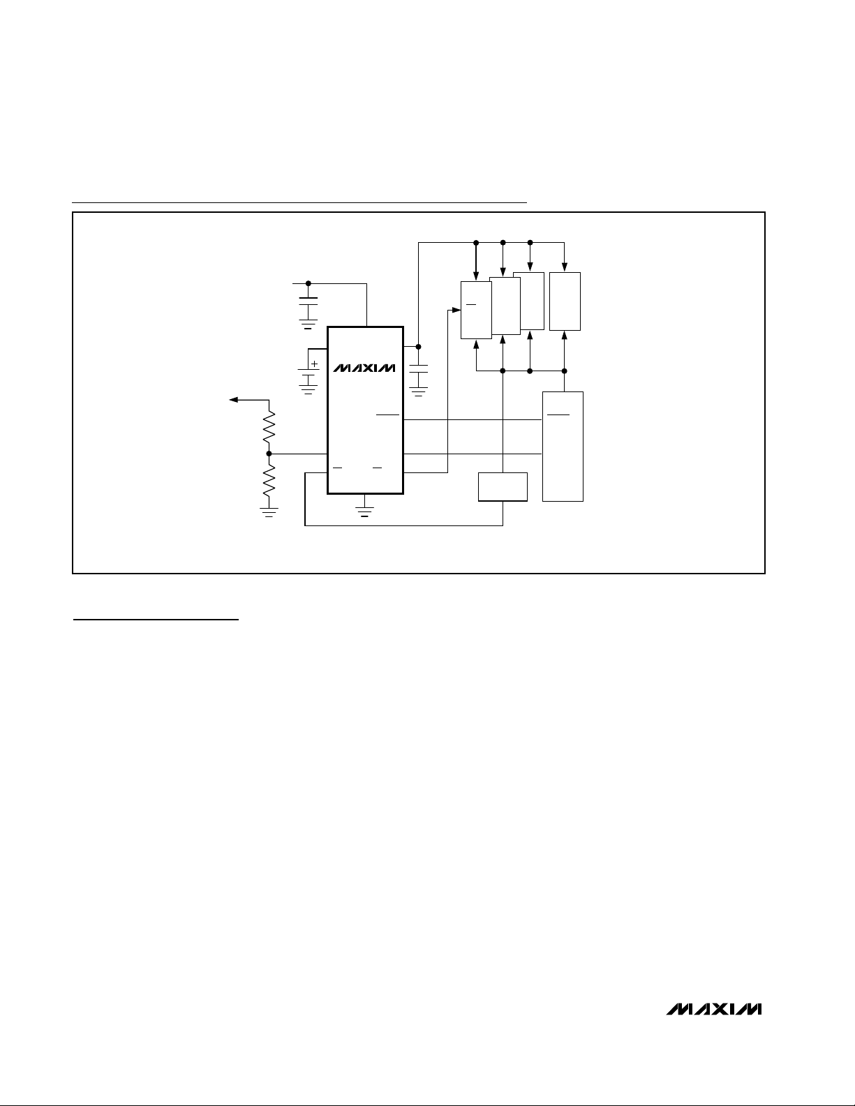
Functional Diagram
BATT ON (MAX6367 ONLY)
1.235V
MAX6365
V
CC
BATT
CE IN
(MAX6365 ONLY)
MR
20k
CHIP-ENABLE
OUTPUT
CONTROL
RESET
GENERATOR
MAX6366
MAX6367
MAX6368
OUT
CE OUT
RESET
(RESET)
(MAX6366 ONLY)
(MAX6368 ONLY)
WDI
RESET IN
1.235V
WATCHDOG
TRANSITION
DETECTOR
GND
WATCHDOG
TIMER

MAX6365–MAX6368
SOT23, Low-Power µP Supervisory Circuits
with Battery Backup and Chip-Enable Gating
_______________________________________________________________________________________ 9
OUT goes high and stays high regardless of any subsequent transitions on CE IN during the reset event.
When CE OUT is disconnected from CE IN, CE OUT is
actively pulled up to OUT.
The propagation delay through the chip-enable circuitry depends on both the source impedance of the drive
to CE IN and the capacitive loading at CE OUT. The
chip-enable propagation delay is production tested
from the 50% point of CE IN to the 50% point of CE
OUT, using a 50Ω driver and 50pF load capacitance.
Minimize the capacitive load at CE OUT to minimize
propagation delay, and use a low-output-impedance
driver.
Backup-Battery Switchover
In a brownout or power failure, it may be necessary to
preserve the contents of the RAM. With a backup battery installed at BATT, the MAX6365–MAX6368 automatically switch the RAM to backup power when V
CC
falls. The MAX6367 has a BATT ON output that goes
high in battery-backup mode. These devices require
two conditions before switching to battery-backup
mode:
1) VCCmust be below the reset threshold.
2) VCCmust be below V
BATT
.
Table 1 lists the status of the inputs and outputs in battery-backup mode. The devices do not power up if the
only voltage source is on BATT. OUT only powers up
from VCCat startup.
Manual Reset Input (MAX6365 Only)
Many µP-based products require manual reset capability, allowing the user or external logic circuitry to initiate a
reset. For the MAX6365, a logic low on MR asserts reset.
Reset remains asserted while MR is low and for a minimum of 150ms (tRP) after it returns high. MR has an internal 20kΩ pullup resistor to VCC. This input can be driven
with TTL/CMOS logic levels or with open-drain/collector
outputs. Connect a normally open momentary switch
from MR to GND to create a manual reset function; external debounce circuitry is not required. If MR is driven
from long cables or the device is used in a noisy environment, connect a 0.1µF capacitor from MR to GND to pro-
vide additional noise immunity.
Figure 1. Reset and Chip-Enable Timing
Table 1. Input and Output Status in
Battery-Backup Mode
PIN STATUS
V
CC
OUT Connected to BATT
BATT
RESET/RESET Asserted
BATT ON High state
MR, RESET IN,
CE IN, WDI
CE OUT Connected to OUT
Disconnected from OUT
Connected to OUT. Current drawn from
the battery is less than 1µA (at V
2.8V, excluding I
Inputs ignored
OUT
) when V
CC
BATT
= 0.
=
V
OR BATT
CC
RESET
THRESHOLD V
TH
CE IN
CE OUT
RESET-TO-CE OUT DELAY (12µs)
RESET
RESET
*
t
RD
t
RD
t
RP
*
IF CE IN GOES HIGH BEFORE RESET ASSERTS,
CE OUT GOES HIGH WITHOUT DELAY AS
CE IN GOES HIGH.
t
RP

MAX6365–MAX6368
SOT23, Low-Power µP Supervisory Circuits
with Battery Backup and Chip-Enable Gating
10 ______________________________________________________________________________________
Watchdog Input (MAX6366 Only)
The watchdog monitors µP activity through the watchdog input (WDI). If the µP becomes inactive, reset
asserts. To use the watchdog function, connect WDI to
a bus line or µP I/O line. A change of state (high to low,
low to high, or a minimum 100ns pulse) resets the
watchdog timer. If WDI remains high or low for longer
than the watchdog timeout period (tWD), the internal
watchdog timer runs out and a reset pulse is triggered
for the reset timeout period (tRP). The internal watchdog
timer clears whenever reset asserts or whenever WDI
sees a rising or falling edge. If WDI remains in either a
high or low state, a reset pulse asserts periodically after
every tWD(Figure 2). Leave WDI unconnected to disable the watchdog function.
BATT ON Indicator (MAX6367 Only)
BATT ON is a push-pull output that drives high when in
battery-backup mode. BATT ON typically sinks 3.2mA
at 0.1V saturation voltage. In battery-backup mode, this
terminal sources approximately 10µA from OUT. Use
BATT ON to indicate battery-switchover status or to
supply base drive to an external pass transistor for
higher current applications (Figure 3).
RESET IN Comparator (MAX6368 Only)
RESET IN is compared to an internal 1.235V reference.
If the voltage at RESET IN is less than 1.235V, reset
asserts. Use the RESET IN comparator as an undervoltage detector to signal a failing power supply or as a
secondary power-supply reset monitor.
To program the reset threshold (V
RTH
) of the secondary
power supply, use the following (see Typical Operating
Circuit):
V
RTH
= V
REF
(R1 / R2 + 1)
where V
REF
= 1.235V. To simplify the resistor selection,
choose a value for R2 and calculate R1:
R1 = R2 [(V
RTH
/ V
REF
) - 1]
Since the input current at RESET IN is 25nA (max),
large values (up to 1MΩ) can be used for R2 with no
significant loss in accuracy. For example, in the Typical
Operating Circuit, the MAX6368 monitors two supply
voltages. To monitor the secondary 5V logic or analog
supply with a 4.60V nominal programmed reset threshold, choose R2 = 100kΩ, and calculate R1 = 273kΩ.
Reset Output
A µP’s reset input starts the µP in a known state. The
MAX6365–MAX6368 µP supervisory circuits assert a
reset to prevent code-execution errors during powerup, power-down, and brownout conditions. RESET is
guaranteed to be a logic low or logic high, depending
on the device chosen (see Ordering Information).
RESET or RESET asserts when VCCis below the reset
threshold and for at least 150ms (t
RP
) after VCCrises
above the reset threshold. RESET or RESET also
asserts when MR is low (MAX6365) and when RESET IN
is less than 1.235V (MAX6368). The MAX6366 watchdog function will cause RESET (or RESET) to assert in
pulses following a watchdog timeout (Figure 2).
Applications Information
Operation Without
a Backup Power Source
The MAX6365–MAX6368 provide battery-backup functions. If a backup power source is not used, connect
BATT to GND and OUT to V
CC
.
Watchdog Software Considerations
One way to help the watchdog timer monitor the software execution more closely is to set and reset the
watchdog at different points in the program rather than
pulsing the watchdog input periodically. Figure 4
shows a flow diagram in which the I/O driving the
Figure 2. MAX6366 Watchdog Timeout Period and Reset Active Time
WDI
t
WD
RESET
t
= WATCHDOG TIMEOUT PERIOD
WD
= RESET TIMEOUT PERIOD
t
RP
t
RP
t
WD
t
RP

MAX6365–MAX6368
SOT23, Low-Power µP Supervisory Circuits
with Battery Backup and Chip-Enable Gating
______________________________________________________________________________________ 11
watchdog is set low in the beginning of the program,
set high at the beginning of every subroutine or loop,
and set low again when the program returns to the
beginning. If the program should hang in any subroutine, the problem would be quickly corrected.
Replacing the Backup Battery
When VCCis above VTH, the backup power source can
be removed without danger of triggering a reset pulse.
The device does not enter battery-backup mode when
VCCstays above the reset threshold voltage.
Negative-Going VCCTransients
These supervisors are relatively immune to short-duration, negative-going V
CC
transients. Resetting the µP
when VCCexperiences only small glitches is usually not
desirable.
The Typical Operating Characteristics section has a
Maximum Transient Duration vs. Reset Threshold
Overdrive graph for which reset is not asserted. The
graph was produced using negative-going V
CC
pulses,
starting at V
CC
and ending below the reset threshold by
the magnitude indicated (reset threshold overdrive).
The graph shows the maximum pulse width that a negative-going VCCtransient can typically have without
triggering a reset pulse. As the amplitude of the transient increases (i.e., goes further below the reset
threshold), the maximum allowable pulse width
decreases. Typically, a VCCtransient that goes 100mV
below the reset threshold and lasts for 30µs will not trigger a reset pulse.
A 0.1µF bypass capacitor mounted close to the V
CC
pin provides additional transient immunity.
Figure 3. MAX6367 BATT ON Driving an External Pass
Transistor
Figure 4. Watchdog Flow Diagram
+2.4V TO +5.5V
0.1µF
START
BATT ON
V
CC
BATT
GND
OUT
CE OUT
MAX6367
ADDRESS
CE IN
RESET
CE
CMOS RAM
DECODE
A0–A15
µP
RESET
SET
WDI
LOW
SUBROUTINE
OR PROGRAM LOOP
SET WDI
HIGH
RETURN
END

MAX6365–MAX6368
SOT23, Low-Power µP Supervisory Circuits
with Battery Backup and Chip-Enable Gating
12 ______________________________________________________________________________________
Reset Threshold Ranges
Device Marking Codes
*These standard versions are available in small quantities through Maxim Distribution. Sample stock is generally held on
standard versions only. Contact factory for availability of nonstandard versions.
SUFFIX
46 4.50 4.63 4.75
44 4.25 4.38 4.50
31 3.00 3.08 3.15
29 2.85 2.93 3.00
26 2.55 2.63 2.70
23 2.25 2.32 2.38
RESET THRESHOLD RANGES (V)
MIN TYP MAX
PART TOP MARK PART TOP MARK PART TOP MARK
MAX6365LKA23 AAAM MAX6366PKA23 AABK MAX6367HKA23 AACI
MAX6365LKA26 AAAL MAX6366PKA26 AABJ MAX6367HKA26 AACH
MAX6365LKA29* AAAK MAX6366PKA29* AABI MAX6367HKA29 AACG
MAX6365LKA31 AAAJ MAX6366PKA31 AABH MAX6367HKA31 AACF
MAX6365LKA44 AAAI MAX6366PKA44 AABG MAX6367HKA44 AACE
MAX6365LKA46* AAAH MAX6366PKA46* AABF MAX6367HKA46* AACD
MAX6365PKA23 AAAS MAX6366HKA23 AABQ MAX6368LKA23 AACO
MAX6365PKA26 AAAR MAX6366HKA26 AABP MAX6368LKA26 AACN
MAX6365PKA29* AAAQ MAX6366HKA29 AABO MAX6368LKA29* AACM
MAX6365PKA31 AAAP MAX6366HKA31 AABN MAX6368LKA31 AACL
MAX6365PKA44 AAAO MAX6366HKA44 AABM MAX6368LKA44 AACK
MAX6365PKA46* AAAN MAX6366HKA46* AABL MAX6368LKA46* AACJ
MAX6365HKA23 AAAY MAX6367LKA23 AABW MAX6368PKA23 AACU
MAX6365HKA26 AAAX MAX6367LKA26 AABV MAX6368PKA26 AACT
MAX6365HKA29 AAAW MAX6367LKA29* AABU MAX6368PKA29* AACS
MAX6365HKA31 AAAV MAX6367LKA31 AABT MAX6368PKA31 AACR
MAX6365HKA44 AAAU MAX6367LKA44 AABS MAX6368PKA44 AACQ
MAX6365HKA46* AAAT MAX6367LKA46* AABR MAX6368PKA46* AACP
MAX6366LKA23 AABE MAX6367PKA23 AACC MAX6368HKA23 AADA
MAX6366LKA26 AABD MAX6367PKA26 AACB MAX6368HKA26 AACZ
MAX6366LKA29* AABC MAX6367PKA29* AACA MAX6368HKA29 AACY
MAX6366LKA31 AABB MAX6367PKA31 AABZ MAX6368HKA31 AACX
MAX6366LKA44 AABA MAX6367PKA44 AABY MAX6368HKA44 AACW
MAX6366LKA46*
AAAZ
MAX6367PKA46*
AABX
MAX6368HKA46*
AACV

MAX6365–MAX6368
SOT23, Low-Power µP Supervisory Circuits
with Battery Backup and Chip-Enable Gating
______________________________________________________________________________________ 13
Pin Configurations (continued)
Selector Guide
RESET
OPENDRAIN
CHIP-
ENABLE
GATING
PART
MANUAL
RESET
INPUT
WATCH-
DOG
INPUT
BATTONRESET
IN
RESET
PUSH-
PULL
RESET
OPENDRAIN
MAX6365LKA__
MAX6365PKA__
MAX6365HKA__
MAX6366LKA__
MAX6366PKA__
MAX6366HKA__
MAX6367LKA__
MAX6367PKA__
MAX6367HKA__
MAX6368LKA__
MAX6368PKA__
MAX6368HKA__
TOP VIEW
RESET, RESET
GND
WDI
1
2
87CE OUT
BATTCE IN
RESET, RESET
MAX6366
3
4
OUT
6
V
5
CC
BATT ON
SOT23
RESET, RESET
1
2
87CE OUT
BATTCE IN
GND
1
2
87CE OUT
BATTCE IN
MAX6367
3
4
OUT
6
V
5
CC
SOT23
MAX6368
GND
RESET IN
3
4
OUT
6
V
5
CC
SOT23
MAX6365–MAX6368
SOT23, Low-Power µP Supervisory Circuits
with Battery Backup and Chip-Enable Gating
14 ______________________________________________________________________________________
Typical Operating Circuit
Chip Information
TRANSISTOR COUNT: 729
PROCESS: CMOS
+2.4V TO +5.5V
0.1µF
BATT
CMOS
RAM
CE
V
CC
OUT
REALTIME
CLOCK
SECONDARY
DC VOLTAGE
R1
RESET IN*
R2
*RESET IN APPLIES TO MAX6368 ONLY.
**WDI APPLIES TO MAX6366 ONLY.
CE IN
MAX6366
MAX6368
CE OUT
GND
RESET
WDI**
0.1µF
A0–A15
RESET
µP
I/O
ADDRESS
DECODE

SOT23, Low-Power µP Supervisory Circuits
with Battery Backup and Chip-Enable Gating
MAX6365–MAX6368
Maxim cannot assume responsibility for use of any circuitry other than circuitry entirely embodied in a Maxim product. No circuit patent licenses are
implied. Maxim reserves the right to change the circuitry and specifications without notice at any time.
Maxim Integrated Products, 120 San Gabriel Drive, Sunnyvale, CA 94086 408-737-7600 ____________________ 15
© 2001 Maxim Integrated Products Printed USA is a registered trademark of Maxim Integrated Products.
Package Information
SOT23, 8L.EPS
 Loading...