

For free samples & the latest literature: http://www.maxim-ic.com, or phone 1-800-998-8800.
For small orders, phone 1-800-835-8769.
General Description
The MAX6351–MAX6360 microprocessor (µP) supervisors with multiple reset voltages significantly improve
system reliability and accuracy compared to separate
ICs or discrete components. If any input supply voltage
drops below its associated preset threshold, all reset
outputs are asserted. In addition, the output(s) is valid
as long as either input supply voltage remains greater
than +1.0V.
All devices in this series have an active-low debounced
manual reset input. In addition, the MAX6358/MAX6359/
MAX6360 offer a watchdog timer input with a 46.4sec
start-up timeout period and a 2.9sec timeout period.
The MAX6355/MAX6356/MAX6357 offer an additional
voltage monitor input to monitor a third voltage.
The MAX6351 features both 3V and 5V active-low pushpull reset outputs. The MAX6353/MAX6356/MAX6359
offer a 5V active-low push-pull reset. The MAX6354/
MAX6357/MAX6360 offer a 3V active-low push-pull
reset. The MAX6352/MAX6355/MAX6358’s reset is
active-low open-drain.
All of these devices are offered with a wide variety of
voltage threshold levels, as shown in the
Voltage
Threshold Levels
table below. They are available in 5and 6-pin SOT23 packages and operate over the
extended (-40°C to +85°C) temperature range.
Applications
Computers Intelligent Instruments
Controllers Multivoltage Systems
Portable/Battery-Powered
Equipment
Features
♦ Precision Monitoring of Multiple +2.5V, +3.0V,
+3.3V, and +5V Power-Supply Voltages
♦ Precision Factory-Set Power-Supply
Reset Thresholds
♦ 20µA Supply Current
♦ 100ms min Power-On Reset Pulse Width
♦ Fully Guaranteed Over Temperature
♦ Guaranteed RESET Valid to V
CC
5 = 1V or
V
CC
3 = 1V
♦ Power-Supply Transient Immunity
♦ No External Components for Dual-Voltage
Systems
♦ Small 5- and 6-Pin SOT23 Packages
♦ Debounced TTL/CMOS-Compatible
Manual-Reset Input
♦ Watchdog Timer
46.4sec Start-Up Timeout
2.9sec Normal Timeout
♦ Low Cost
MAX6351–MAX6360
Dual/Triple-Voltage
µP Supervisory Circuits
________________________________________________________________
Maxim Integrated Products
1
19-1508; Rev 1; 10/99
*
The _ _ are placeholders for the threshold voltage levels of the
devices. Substitute the part number suffix in the Voltage
Threshold Levels table for the desired voltage level. There are
two standard versions for each of the above part numbers. All
devices are available in tape-and-reel only.
Ordering Information
PART*
MAX6351_ _UT-T
MAX6352_ _UK-T
MAX6353_ _UK-T
-40°C to +85°C
-40°C to +85°C
-40°C to +85°C
TEMP. RANGE PIN-PACKAGE
6 SOT23-6
5 SOT23-5
5 SOT23-5
MAX6354_ _UK-T
MAX6355_ _UT-T
MAX6356_ _UT-T
-40°C to +85°C
-40°C to +85°C
-40°C to +85°C 5 SOT23-5
6 SOT23-6
6 SOT23-6
MAX6357_ _UT-T
MAX6358_ _UT-T
MAX6359_ _UT-T
-40°C to +85°C
-40°C to +85°C
-40°C to +85°C 6 SOT23-6
6 SOT23-6
6 SOT23-6
MAX6360_ _UT-T
-40°C to +85°C 6 SOT23-6
PART NO.
SUFFIX
(_ _)
VCC5 NOMINAL
VOLTAGE
THRESHOLD (V)
VCC3 NOMINAL
VOLTAGE
THRESHOLD (V)
LT 4.63 3.08
LS
LR 4.63 2.63
4.63 2.93
MT
MS 4.38 2.93
MR
4.38 3.08
TY 3.08 2.19
4.38 2.63
SY 2.93 2.19
Note: Standard versions are shown in bold and have a required
order increment of 2500 pieces. Sample stock is generally held on
the standard versions only. The required order increment for nonstandard versions is 10,000 pieces. Contact factory for availability.
__________Voltage Threshold Levels
Pin Configurations appear at end of data sheet.
Selector Guide appears at end of data sheet.
查询MAX6351供应商
MAX6351–MAX6360
Dual/Triple-Voltage
µP Supervisory Circuits
2 _______________________________________________________________________________________
ABSOLUTE MAXIMUM RATINGS
Stresses beyond those listed under “Absolute Maximum Ratings” may cause permanent damage to the device. These are stress ratings only, and functional
operation of the device at these or any other conditions beyond those indicated in the operational sections of the specifications is not implied. Exposure to
absolute maximum rating conditions for extended periods may affect device reliability.
VCC5, VCC3 to GND .................................................-0.3V to +6V
RST (MAX6352/55/58)............................................. -0.3V to +6V
RST, MR, WDI, RST5, RSTIN
(MAX6351/53/56/59).............................-0.3V to (V
CC
5 + 0.3V)
RST, RST3 (MAX6351/54/57/60) .................-3V to (V
CC
3 + 0.3V)
Input/Output Current, All Pins .............................................20mA
Continuous Power Dissipation (T
A
= +70°C)
5-Pin SOT23-5 (derate 7.1mW/°C above +70°C) ........571mW
6-Pin SOT23-6 (derate 7.1mW/°C above +70°C) ........571mW
Operating Temperature Range ...........................-40°C to +85°C
Storage Temperature Range .............................-65°C to +150°C
Lead Temperature (soldering, 10sec) .............................+300°C
100mV overdrive
VCC5 = 5.5V, VCC3 = 3.6V, all I/O pins open
VCCto Reset Delay
TA= -40°C to +85°C
MAX63_ _ _Y
TA= 0°C to +70°C
MAX63_ _ _R
MAX63_ _S_
MAX63_ _ _S
MAX63_ _T_
MAX63_ _ _T
MAX63_ _M_
CONDITIONS
µs
20
V
VTH/500
Reset Threshold Hysteresis
ppm/°C
20
∆VTH/°CReset Threshold Tempco
2.13 2.25
2.16 2.19 2.22
2.55 2.70
2.58 2.63 2.68
2.85 3.00
2.88 2.93 2.98
3.00 3.15
V
3.03 3.08 3.14
VTH3VCC3 Threshold (Note 3)
2.85 3.00
µA
20 50
ICC5 +
ICC3
Supply Current
1.2 5.5
V
1.0 5.5
V
CC
Supply Voltage Range (Note 2)
2.88 2.93 2.98
3.00 3.15
3.03 3.08 3.14
4.25 4.50
V
4.54 4.63 4.72
VTH5VCC5 Threshold (Note 3)
4.5 4.75
4.3 4.38 4.46
UNITSMIN TYP MAXSYMBOLPARAMETER
VCC5 > VTH5
(MAX)
, VCC3 > VTH3
(MAX)
VCC5 or VCC3 ≥ 2.7V, I
SINK
= 1.2mA
VCC5 or VCC3 ≥ 4.5V, I
SINK
= 3.2mA
VCC5 or VCC3 < 1V, I
SINK
= 50µA,
TA= 0°C to +70°C
ms
100 180 280
t
RP
Reset Timeout Period
0.3
0.4
V
0.3
TA= +25°C
MAX63_ _L_
TA= -40°C to +85°C
TA= +25°C
TA= -40°C to +85°C
TA= +25°C
TA= -40°C to +85°C
TA= +25°C
TA= -40°C to +85°C
TA= +25°C
TA= -40°C to +85°C
TA= +25°C
TA= -40°C to +85°C
TA= +25°C
TA= -40°C to +85°C
TA= +25°C
TA= -40°C to +85°C
ELECTRICAL CHARACTERISTICS
(VCC3 = VCC5 = +1.2V to +5.5V, TA= -40°C to +85°C, unless otherwise noted. Typical values are at TA = +25°C.) (Note 1)
VCC5 or VCC3 < 1.2V, I
SINK
= 50µA
V
OL
RESET Output Voltage Low
0.3
V
MAX6351–MAX6360
Dual/Triple-Voltage
µP Supervisory Circuits
_______________________________________________________________________________________ 3
Note 1: Overtemperature limits are guaranteed by design and not production tested.
Note 2: The reset output is guaranteed to be in the correct state if either V
CC
3 or VCC5 is within its specified region of operation.
Note 3: The reset output(s) is asserted if either V
CC
5 or VCC3 drops below its associated trip point.
Note 4: Guaranteed by design. Not production tested.
Note 5: WDI is internally serviced within the watchdog timeout period if WDI is left unconnected.
Note 6: The WDI input current is specified as the average input current when the WDI input is driven high or low.
MAX6351/MAX6353/
MAX6354/MAX6356/
MAX6357/MAX6359/
MAX6360
(_Y versions only),
VCC5 > VTH5
(MAX)
,
VCC3 > VTH3
(MAX)
CONDITIONS UNITSMIN TYP MAXSYMBOLPARAMETER
MAX63_ _ _Y, VCC5 > VTH5
(MAX)
MAX63_ _ _Y, VCC5 > VTH5
(MAX)
MAX63_ _L_, MAX63_ _M_, VCC5 > VTH5
(MAX)
MAX63_ _L_, MAX63_ _M_, VCC5 > VTH5
(MAX)
V
WDI
= 0
V
WDI
= V
CC
First timeout period after reset
MAX6351/MAX6353/
MAX6354/MAX6356/
MAX6357/MAX6359/
MAX6360
(L_, M_ versions only),
VCC5 > VTH5
(MAX)
,
VCC3 > VTH3
(MAX)
VCC3 = 5V
VIL= 0.4V, VIH= 0.8V
CC
µs
10
t
RP
MR Minimum Pulse Width
kΩ
32 63.5 100
MR Pull-Up Resistance
0.7V
CC
2.3
V
IL
0.8
MR Input
V
-20 -15
µA
120 160
WDI Input Current (Note 6)
0.7V
CC
V
IH
V
0.3V
CC
V
IL
WDI Input Threshold (Note 5)
ns
50
t
WDI
WDI Pulse Width (Note 4)
1.6 2.9 4.5
sec
25.6 46.4 72.0
t
WD
Watchdog Timeout Period
V
CC
- 1.5
0.8V
CC
0 < V
RISTIN
< VCC5 - 0.3V
VCC5 > VTH5
(MAX),
VCC3 > VTH3
(MAX)
mV
2.5
RSTIN Hysteresis
nA
-25 25
I
RSTIN
RSTIN Input Current
1.19 1.25
V
1.20 1.22 1.24
V
RSTIN
RSTIN Input Threshold
µs
0.1
t
MD
MR to Reset Delay
ns
100
MR Glitch Rejection
TA= +25°C
TA= -40°C to +85°C
ELECTRICAL CHARACTERISTICS (continued)
(VCC3 = VCC5 = +1.2V to +5.5V, TA= -40°C to +85°C, unless otherwise noted. Typical values are at TA= +25°C.) (Note 1)
WATCHDOG INPUT (MAX6358/MAX6359/MAX6360)
MANUAL RESET INPUT
ADJUSTABLE RESET COMPARATOR INPUT (MAX6355/MAX6356/MAX6357)
I
SOURCE
= 500µA
V
OH
RESET Output Voltage High
I
SOURCE
= 800µA
V
After first WDI falling edge
0.3V
CC
V
IL
V
IH
V
IH

MAX6351–MAX6360
Dual/Triple-Voltage
µP Supervisory Circuits
4 _______________________________________________________________________________________
Typical Operating Characteristics
(V
CC
= +5V, TA= +25°C, unless otherwise noted.)
0
5
10
15
20
-40 10-15 35 60 85
SUPPLY CURRENT vs. TEMPERATURE
MAX6351/60-01
TEMPERATURE (°C)
SUPPLY CURRENT (µA)
ICC5 (VCC5 = 5.0V, VCC3 = 3.3V)
ICC3 (VCC5 = 5.0V, VCC3 = 3.3V)
ICC3 (VCC5 = 3.3V, VCC3 = 2.5V)
ICC5 (VCC5 = 3.3V, VCC3 = 2.5V)
VCC5 (V)
RESET vs. VCC5 (VCC3 = 3V)
V
TH
0
1.0
0.5
2.0
1.5
3.0
2.5
3.5
4.5
4.0
5.0
0 1.0 1.5 2.00.5 2.5 3.0 3.5 4.54.0 5.0
MAX6351/60-02
RESET (V)
0
1.0
0.5
2.0
1.5
3.0
2.5
3.5
4.5
4.0
5.0
0 1.0 1.5 2.00.5 2.5 3.0 3.5 4.54.0 5.0
MAX6351/60-03
VCC5 (V)
RESET (V)
RESET vs. VCC5 (VCC3 = GND)
MAX6351
MAX6360
10k
V
CC
5 OR VCC3
V
CC
RST5
RST3
RST
0.80
0.90
0.85
1.00
0.95
1.05
1.10
1.15
1.20
-60 -20 0-40 20 40 60 80 100
NORMALIZED RESET/WATCHDOG
PERIOD vs. TEMPERATURE
MAX6351/60-04
TEMPERATURE (°C)
NORMALIZED PERIOD
OPEN-DRAIN
OUTPUT
0
0
0
5V
3V
5V PUSH-PULL
OUTPUT
3V PUSH-PULL
OUTPUT
5V
PULL-UP CHARACTERISTICS
MAX6351/60-07
400ns/div
300
0
0.01 0.1 1
MAXIMUM VCC TRANSIENT DURATION
vs. RESET THRESHOLD OVERDRIVE
100
50
MAX6351/60-05
RESET THRESHOLD OVERDRIVE, V
RST
- V
CC
(V)
TRANSIENT DURATION (µs)
150
200
250
RESET OCCURS ABOVE LINE
0
50
100
150
200
250
0 0.4 0.50.2 0.30.1 0.6 0.7 0.8 0.9 1.0
RESET DELAY vs.
RESET THRESHOLD OVERDRIVE
MAX6351/60-06
RESET THRESHOLD OVERDRIVE, V
RST
- V
CC
(V)
RESET DELAY (µs)
DELAY FROM FALL OF VCC5
DELAY FROM FALL OF VCC3
0
5V
PULL-DOWN CHARACTERISTICS
AND MANUAL RESET DELAY
40ns/div
0
5V
MR
MAX6351/60-08
0
0
5V
5V
OPEN-DRAIN
OUTPUT
5V PUSH-PULL
OUTPUT
3V PUSH-PULL
OUTPUT

MAX6351–MAX6360
Dual/Triple-Voltage
µP Supervisory Circuits
_______________________________________________________________________________________ 5
— 1 1
2 2 2
— — 5
5 — —
4 4 4
3 3 3
6 5 6
— — —
Pin Description
FUNCTION
Active-Low Reset Output. Open-drain for the
MAX6352/MAX6355/MAX6358, 5V push-pull for the
MAX6353/MAX6356/MAX6359, and 3V push-pull for
the MAX6354/MAX6357/MAX6360.
Ground
Undervoltage Reset Comparator Input. Asserts
reset when the monitored voltage falls below 1.23V.
Set the reset threshold with an external resistordivider. Connect to VCC5 if unused. V
RSTIN
must be
below VCC5.
Active-Low, 3V CMOS Reset Output
+3.3V/+3.0V Supply Input. Powers the device when
it is above VCC5 and monitors its own voltage.
Manual-Reset Input. Pull low to force a reset. RST,
RST5, and RST3 remain active as long as MR is low
and for the timeout period after MR goes high.
Leave unconnected or connect to V
CC
5 if unused.
VMRmust be below VCC5.
+5V Supply Input. Powers the device when it is
above VCC3 and monitors its own voltage.
Watchdog Input. If WDI remains either high or low
longer than the timeout period, then reset is triggered. The timer clears when reset is asserted or
whenever WDI sees a rising or falling edge. Leave
floating to disable it if unused.
1
2
—
—
4
3
6
5
NAME
RST
GND
RSTIN
RST3
VCC3
MR
VCC5
WDI
1 — — Active-Low, 5V CMOS Reset Output—
RST5
MAX6351
MAX6352
MAX6353
MAX6354
MAX6355
MAX6356
MAX6357
MAX6358
MAX6359
MAX6360
PIN

6 _______________________________________________________________________________________
MAX6351–MAX6360
Detailed Description
Supply Voltages
The MAX6351–MAX6360 microprocessor (µP) supervisory circuits maintain system integrity by alerting the µP to
fault conditions. These ICs monitor multiple-supply systems and derive their internal power from the highest voltage source present at VCC5 and VCC3. In addition, the
output reset state is guaranteed to remain viable while
either VCC5 or VCC3 is above +1V.
Threshold Levels
All the possible input voltage threshold level combinations are indicated by a two-letter code in
Voltage
Threshold Levels
. The two standard combinations are
LS and SY. LS parts monitor one +5V ±5% supply and
one +3.3V ±10% supply. SY parts monitor one +3.3V
±10% supply and one +2.5V ±10% supply. The other
combinations also monitor +5V ±10% supplies, +3.3V
±5% supplies, and +3V ±5% supplies.
Reset Outputs
The MAX6351 provides a 5V active-low reset and a 3V
active-low reset. The MAX6353/MAX6356/MAX6359 provide a 5V active-low push-pull reset and the MAX6354/
MAX6357/MAX6360 provide a 3V active-low push-pull
reset. The MAX6353/MAX6355/MAX6358 provide an
active-low open-drain reset. The higher input voltages of
VCC5 and VCC3 maintain the sinking capability of the
low reset-output state. The reset outputs are maintained
as long as either supply is above +1V.
Negative-Going VCCTransients
The MAX6351–MAX6360 are designed to ignore short
negative-going VCC5 and VCC3 transients. See
Typical
Operating Characteristics
for a glitch immunity graph.
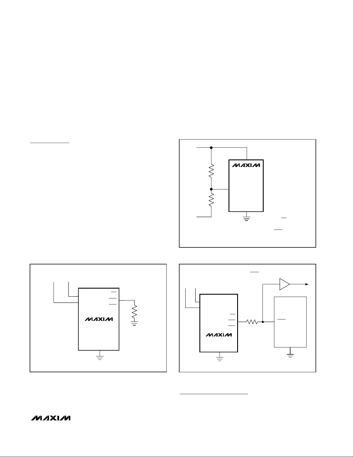
Third Input Voltage
(MAX6355/MAX6356/MAX6357)
The MAX6355/MAX6356/MAX6357 provide an additional input to monitor a third voltage. The threshold voltage
at RSTIN is typically 1.22V. To monitor a voltage higher
than 1.22V, connect a resistor-divider to the circuit as
shown in Figure 2. The threshold at V3is:
Note that RSTIN is powered by VCC5, and its voltage
must therefore remain lower than VCC5.
V 1.22
R1 R2
R2
3TH
=
+
Dual/Triple-Voltage
µP Supervisory Circuits
Figure 1. Functional Diagram
Figure 2. Monitoring a Third Voltage
3
MR
5(5) 6
V
CC
3
V
CC
(RSTIN)
VTH5
V
TH
3
4
(5)
GLITCH
FILTER
RESET
GENERATOR
RST (1)
RST3 (5)
(1)RST5
1.22V
(5)
(WDI)
2
GND
NOTE: PIN 1 IS RST5 FOR THE MAX6351 AND RST FOR THE
MAX6352–MAX6360. PIN 5 IS RST3 FOR THE MAX6351, RSTIN
FOR THE MAX6355/56/57, WDI FOR THE MAX6358/59/60,
FOR THE MAX6352/53/54.
AND V
CC
WATCHDOG
TIMER
MAX6351–MAX6360
V3
R1
R2
V
5 ≥ V
CC
RSTIN
MAX6355
MAX6356
MAX6357
RSTIN
Watchdog Input
(MAX6358/MAX6359/MAX6360)
The MAX6358/MAX6359/MAX6360 include a WDI to
provide a reset if the µP goes into an infinite loop. After
a reset, the start-up timeout period and the initial timeout period is nominally 46.4sec to allow the µP time to
initialize. After the first transition on the WDI and after
any toggle of the watchdog thereafter, the timeout period is nominally 2.9sec.
Applications Information
Ensuring a Valid
RESET
Output
Down to V
CC
= 0
In some systems, it is necessary to ensure a valid reset
even if VCCfalls to 0. In these applications, use the circuit shown in Figure 3. Note that this configuration does
not work for the open-drain outputs of the MAX6352/
MAX6355/MAX6358.
Monitoring a Negative Voltage
To monitor a negative supply rail using RSTIN or the
MAX6355/MAX6356/MAX6357, use the circuit shown in
Figure 4. In this configuration, a reset is issued when
the negative supply falls below V
INTH
.
Interfacing to µPs with
Bidirectional Reset Pins
Microprocessors with bidirectional reset pins will contend with the push-pull outputs of these devices. To
prevent this, connect a 4.7kΩ resistor between RESET
and the µP’s reset I/O port, as shown in Figure 5. Buffer
RESET as shown in the figure if this reset is used by
other components in the system.
MAX6351–MAX6360
Dual/Triple-Voltage
µP Supervisory Circuits
_______________________________________________________________________________________ 7
Figure 4. Monitoring a Negative Voltage
Figure 3. Ensuring a Valid Reset Low to VCC5 and VCC3 = 0
Figure 5. Interfacing to µPs with Bidirectional Reset I/O
Chip Information
TRANSISTOR COUNT: 855
VCC5
R1
R2
V
IN
RSTIN
MAX6355
MAX6356
MAX6357
INTH
VCC5
VCC5
≥ ≥ V
V
INR
RSTIN
R1
1
R
2
R2
= 1.22 - (VCC5 - 1.22)
V
+3.3V/+3V +5V
V
CC
VCC3
5
RST
RST3
RST5
100k
MAX6351–MAX6360
GND
BUFFERED RESET TO OTHER SYSTEM COMPONENTS
5
V
3
V
CC
CC
V
5
CC
VCC3
RST
RST3
RST5
MAX6351–MAX6360
GND
4.7k
µP
RESET
GND

MAX6351–MAX6360
Dual/Triple-Voltage
µP Supervisory Circuits
Maxim cannot assume responsibility for use of any circuitry other than circuitry entirely embodied in a Maxim product. No circuit patent licenses are
implied. Maxim reserves the right to change the circuitry and specifications without notice at any time.
8
_____________________Maxim Integrated Products, 120 San Gabriel Drive, Sunnyvale, CA 94086 408-737-7600
© 1999 Maxim Integrated Products Printed USA is a registered trademark of Maxim Integrated Products.
Pin Configurations
✔
✔
—
✔
—
——
✔
26MAX6360
26MAX6359
—
—
—
—
—
—
WATCHDOG
TIMER
✔
—
——
—
✔
—
—
✔
✔
✔
——
—
✔
—
——
✔
OPEN-DRAIN
RESET
✔
—
3V RESET
—
—
✔✔
5V RESET
—
36
36MAX6357
25
MAX6356
36MAX6355
MAX6354
25
25MAX6353
NUMBER OF
SUPPLIES
MONITORED
26
PIN
COUNT
MAX6352
26MAX6351
PART
MAX6358
✔
✔
✔
✔
✔
✔
✔
✔
MANUAL
RESET
✔
✔
Selector Guide
TOP VIEW
16VCC5
RST5
15VCC5RST*
GND
MAX6351
2
34
5 RST3
V
CC
3MR
SOT23-6
16VCC5
RST*
2
MAX6355
MAX6356
5 RSTIN
GND
MAX6357
34
SOT23-6
*MAX6355: OPEN-DRAIN OUTPUT
*MAX6356: 5V PUSH-PULL OUTPUT
*MAX6357: 3V PUSH-PULL OUTPUT
V
3MR
CC
2
MAX6352
MAX6353
GND
MAX6354
34
SOT23-5
16VCC5
RST*
2
MAX6358
MAX6359
5 WDI
GND
MAX6360
34
V
SOT23-6
*MAX6352: OPEN-DRAIN OUTPUT
*MAX6353: 5V PUSH-PULL OUTPUT
*MAX6354: 3V PUSH-PULL OUTPUT
3MR
V
CC
*MAX6358: OPEN-DRAIN OUTPUT
*MAX6359: 5V PUSH-PULL OUTPUT
*MAX6360: 3V PUSH-PULL OUTPUT
3MR
CC
 Loading...