For free samples & the latest literature: http://www.maxim-ic.com, or phone 1-800-998-8800.
For small orders, phone 1-800-835-8769.
General Description
The MAX6342–MAX6345 family of microprocessor (µP)
supervisory circuits monitors power supplies in digital systems. These devices significantly improve system reliability and accuracy compared to separate ICs or discrete
components.
The MAX6342–MAX6345 provide factory-trimmed V
CC
reset threshold voltages from 2.33V to 4.63V and operate
with supply voltages between +1V and +5.5V. A +1.25V
threshold detector allows for a power-fail warning, for lowbattery detection, or for monitoring another power supply.
The MAX6342 contains an MR input and an active-low
push-pull reset. The MAX6343 and MAX6344 are identical
to the MAX6342 except they provide an active-low, opendrain reset and an active-high, push-pull reset, respectively. The MAX6345 provides a second reset output in place
of the MR input to give it an active-high push-pull reset
and an active-low push-pull reset.
All of the devices are packaged in a miniature 6-pin
SOT23.
Applications
Portable Computers
Telecom Equipment
Networking Equipment
Portable/Battery-Powered Equipment
Multivoltage Systems
Embedded Control Systems
Features
♦ Small 6-Pin SOT23 Package
♦ Precision Factory-Set V
CC
Reset Thresholds
Between 2.33V and 4.63V
♦ Guaranteed RESET Valid to V
CC
= +1V
♦ 100ms min Reset Pulse Width
♦ Debounced CMOS-Compatible Manual-Reset
Input
♦ Voltage Monitor for Power-Fail or Low-Battery
Warning
MAX6342–MAX6345
6-Pin µP Reset Circuit with
Power-Fail Comparator
________________________________________________________________
Maxim Integrated Products
1
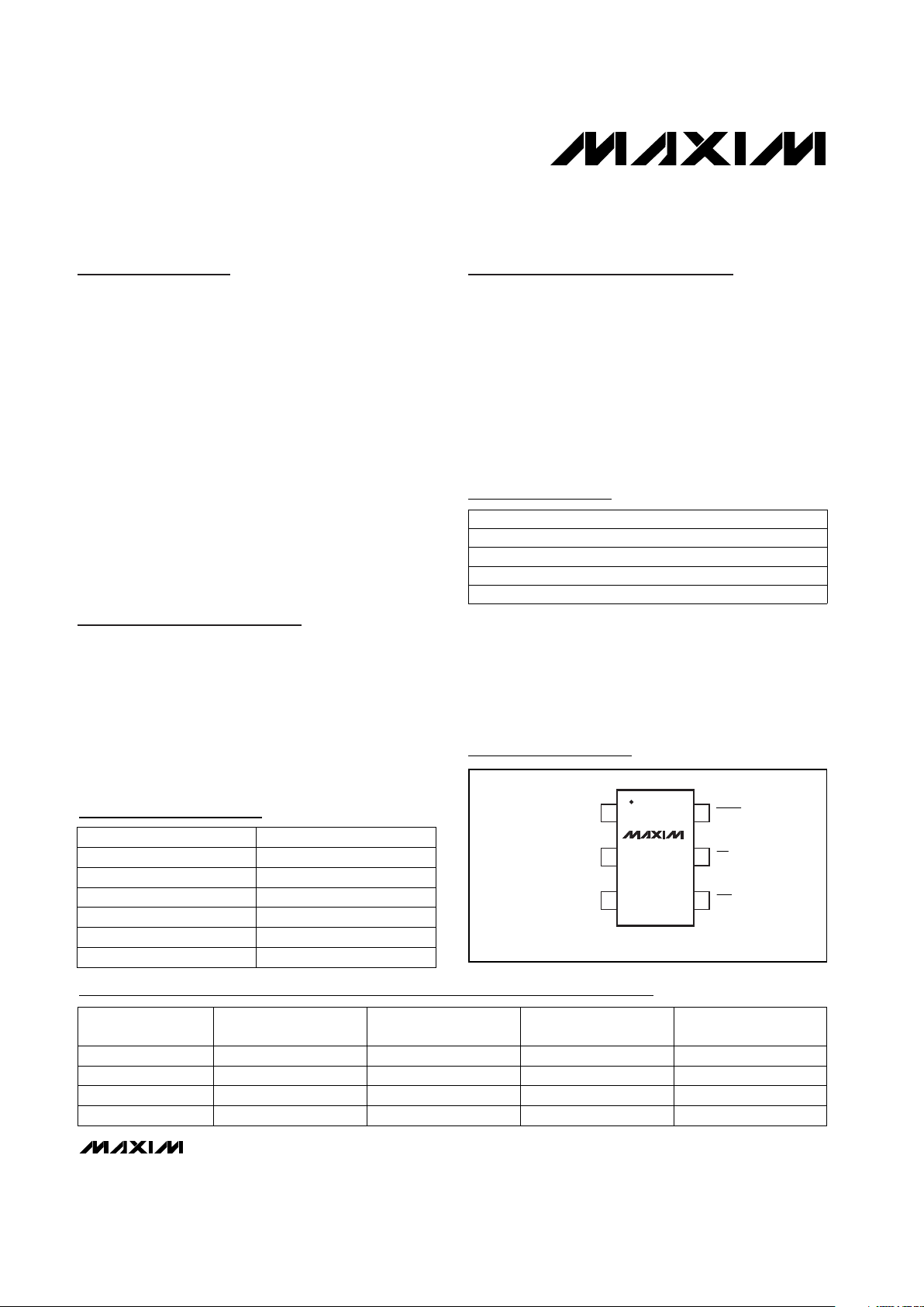
GND
PFI
16
5
V
CC
( ) ARE FOR MAX6344 ONLY.
TOP VIEW
2
34
RESET (RESET)
PFO
MR
MAX6342
MAX6343
MAX6344
SOT23-6
Selector Guide 1
Selector Guide 2
19-1568; Rev 0; 10/99
PART
MAX6342_UT-T
MAX6343_UT-T
MAX6344_UT-T
-40°C to +85°C
-40°C to +85°C
-40°C to +85°C
TEMP. RANGE PIN-PACKAGE
6 SOT23-6
6 SOT23-6
6 SOT23-6
Note:
The MAX6342–MAX6345 are available with factory-set
reset thresholds from 2.33V to 4.63V (see Selector Guides 1, 2).
Insert the letter corresponding to the desired nominal reset
threshold into the blank following the part number. There is a
2500 piece order increment required for the SOT package. SOT
Top Marks table appears at end of data sheet. All versions of
these products may not be available at time of announcement.
Contact factory for availability.
Pin Configurations
Ordering Information
MAX6345_UT-T
-40°C to +85°C 6 SOT23-6
SUFFIX RESET THRESHOLD (V)
L
4.63
M 4.38
T 3.08
S 2.93
R 2.63
Z 2.33
PART
PUSH-PULL
RESET OUTPUT
OPEN-DRAIN
RESET OUTPUT
PUSH-PULL RESET
OUTPUT
MAX6342
✔
— —
MAX6343 —
✔
—
MAX6344 — —
✔
MAX6345
✔
—
✔
MANUAL-RESET
INPUT
✔
✔
✔
—
Typical Operating Circuit appears at end of data sheet.
Pin Configurations continued at end of data sheet.

V
MAX6342–MAX6345
6-Pin µP Reset Circuit with
Power-Fail Comparator
2 _______________________________________________________________________________________
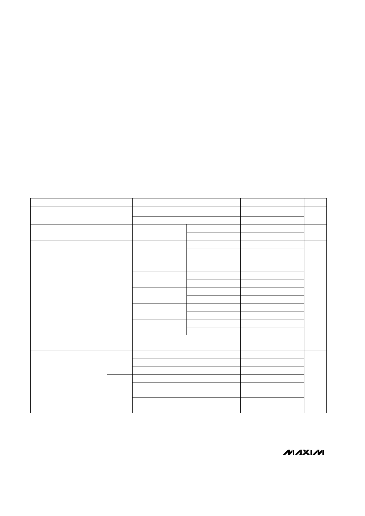
ABSOLUTE MAXIMUM RATINGS
ELECTRICAL CHARACTERISTICS
(VCC= +1.0V to +5.5V, TA= -40°C to +85°C, unless otherwise noted. Typical values are at TA= +25°C and VCC= +3V.) (Note 1)
Stresses beyond those listed under “Absolute Maximum Ratings” may cause permanent damage to the device. These are stress ratings only, and functional
operation of the device at these or any other conditions beyond those indicated in the operational sections of the specifications is not implied. Exposure to
absolute maximum rating conditions for extended periods may affect device reliability.
VCCto GND..............................................................-0.3V to +6V
RESET, RESET
(MAX6342/MAX6344/MAX6345) ......... -0.3V to (V
CC
+ 0.3V)
RESET (MAX6343)................................................... -0.3V to +6V
MR, PFI, PFO ..............................................-0.3V to (V
CC
+ 0.3V)
Input Current, V
CC
..............................................................50mA
Output Current, RESET, RESET ..........................................50mA
Continuous Power Dissipation (T
A
= +70°C)
6-Pin SOT23 (derate 4mW/°C above +70°C).............320mW
Operating Temperature Range ...........................-40°C to +85°C
Junction Temperature......................................................+150°C
Storage Temperature Range .............................-65°C to +150°C
Lead Temperature Range (soldering, 10sec)................. +300°C
VCC> 2.7V, I
SOURCE
= 500µA
(MAX6342/MAX6345 only)
VCC> 1.2V, I
SOURCE
= 50µA
VCC> 4.5V, I
SINK
= 3.2mA
VCC> 2.7V, I
SINK
= 1.2mA
TA= -40°C to +85°C
VCC> 1.2V, I
SINK
= 100µA
TA= 0°C to +70°C
VCC= VTHto (VTH- 100mV)
µA
MAX634_S
MAX634_Z
MAX634_T
No load
MAX634_L
MAX634_R
MAX634_M
CONDITIONS
0.8 · V
CC
0.8 · V
CC
0.4
0.3
V
0.4
V
OL
ms
100 180 280
t
RP
Reset Timeout Period
µs
20
VCCto Reset Delay
V
2.25 2.38
2.30 2.33 2.36
2.55 2.70
2.59 2.63 2.67
2.85 3.00
25 40
I
CC
Supply Current
1.2 5.5
V
1.0 5.5
V
CC
Supply Voltage Range
2.89 2.93 2.97
3.00 3.15
3.03 3.08 3.13
4.25 4.50
30 50
4.56 4.63 4.70
V
TH
Reset Threshold
4.50 4.75
4.31 4.38 4.45
UNITSMIN TYP MAXSYMBOLPARAMETER
TA= +25°C
TA= -40°C to +85°C
TA= +25°C
TA= -40°C to +85°C
TA= +25°C
TA= -40°C to +85°C
TA= +25°C
TA= -40°C to +85°C
TA= +25°C
TA= -40°C to +85°C
TA= +25°C
TA= -40°C to +85°C
VCC= 3V
VCC= 5.5V
VCC> 4.5V, I
SOURCE
= 800µA
(MAX6342/MAX6345 only)
0.8 · V
CC
V
OH
RESET and RESET Outputs
Drive Capability (Note 2)

MAX6342–MAX6345
6-Pin µP Reset Circuit with
Power-Fail Comparator
_______________________________________________________________________________________ 3
ELECTRICAL CHARACTERISTICS (continued)
(VCC= +1.0V to +5.5V, TA= -40°C to +85°C, unless otherwise noted. Typical values are at TA= +25°C and VCC= +3V.) (Note 1)
CONDITIONS UNITSMIN TYP MAXSYMBOLPARAMETER
MAX6343 only, VCC> V
TH(MAX)
MR Pull-Up Resistance
V
0.7 · V
CC
V
IH
MR Input High
V
0.3 · V
CC
V
IL
MR Input Low
µA
1
I
LKG
Open-Drain RESET Output
Leakage Current
60
kΩ
MR Minimum Pulse Width
1
µs
MR Glitch Rejection
0.1
µs
MR to Reset Delay
0.2
µs
PFI Input Threshold
1.2 1.25 1.3
V
PFI Leakage Current
±0.01 ±25
nA
PFO Output Voltage
V
OL
VCC= 4.5V, I
SINK
= 3.2mA
0.4
V
PFO Output Voltage
V
OH
VCC= 4.5V, I
SOURCE
= 800µA
0.8 · V
CC
PFO Output Short-Circuit
Current
Output sink current
20
mA
Output source current
5
PFI to PFO Delay
V
OVERDRIVE
= 15mV
3
µs
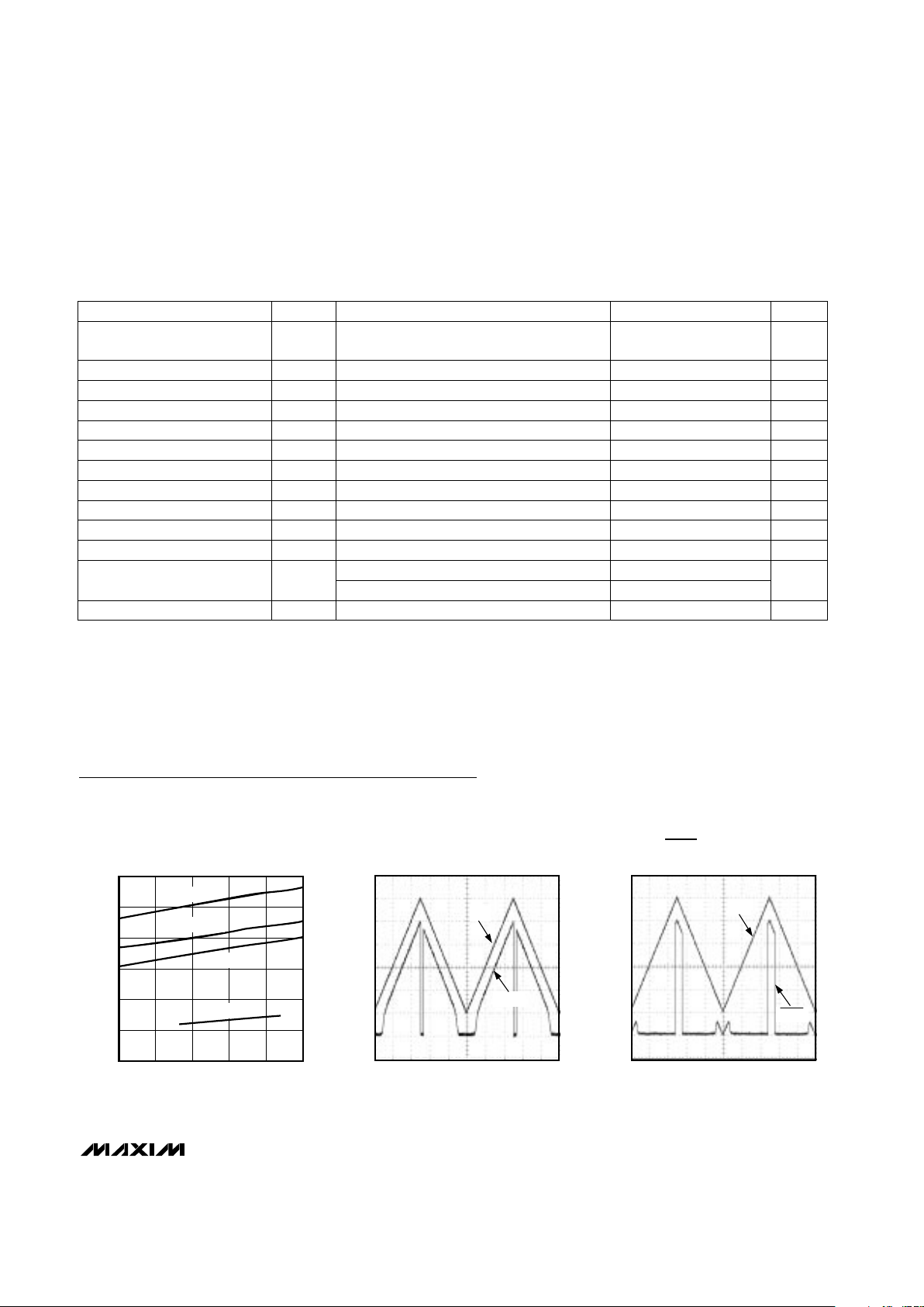
Typical Operating Characteristics
(V
PFI
= VCC= +5V, TA= +25°C, unless otherwise noted.)
0
10
5
20
15
25
30
-40 10-15 35 60 85
SUPPLY CURRENT vs. SUPPLY VOLTAGE
AND TEMPERATURE
MAX6342-01
TEMPERATURE (°C)
SUPPLY CURRENT (µA)
VCC = 5V
VCC = 3.3V
VCC = 2.5V
VCC = 1V
0
0
1sec/div
MAX6342-02
MAX6344L/MAX6345L
RESET OUTPUT VOLTAGE
vs. SUPPLY VOLTAGE
V
CC
RESET
1V/div
0
0
1sec/div
MAX6342-03
MAX6342M/MAX6345M
RESET OUTPUT VOLTAGE
vs. SUPPLY VOLTAGE
V
CC
RESET
1V/div
V
Note 1: Overtemperature limits are guaranteed by design and not production tested.
Note 2: Apply to each part in accordance with threshold voltage, output configuration, and manual reset status selected.
 Loading...