

Datasheet MAX6343ZUT-T, MAX6343LUT-T, MAX6343MUT-T, MAX6343RUT-T, MAX6343SUT-T Datasheet (Maxim)
...
For free samples & the latest literature: http://www.maxim-ic.com, or phone 1-800-998-8800.
For small orders, phone 1-800-835-8769.
General Description
The MAX6342–MAX6345 family of microprocessor (µP)
supervisory circuits monitors power supplies in digital systems. These devices significantly improve system reliability and accuracy compared to separate ICs or discrete
components.
The MAX6342–MAX6345 provide factory-trimmed V
CC
reset threshold voltages from 2.33V to 4.63V and operate
with supply voltages between +1V and +5.5V. A +1.25V
threshold detector allows for a power-fail warning, for lowbattery detection, or for monitoring another power supply.
The MAX6342 contains an MR input and an active-low
push-pull reset. The MAX6343 and MAX6344 are identical
to the MAX6342 except they provide an active-low, opendrain reset and an active-high, push-pull reset, respectively. The MAX6345 provides a second reset output in place
of the MR input to give it an active-high push-pull reset
and an active-low push-pull reset.
All of the devices are packaged in a miniature 6-pin
SOT23.
Applications
Portable Computers
Telecom Equipment
Networking Equipment
Portable/Battery-Powered Equipment
Multivoltage Systems
Embedded Control Systems
Features
♦ Small 6-Pin SOT23 Package
♦ Precision Factory-Set V
CC
Reset Thresholds
Between 2.33V and 4.63V
♦ Guaranteed RESET Valid to V
CC
= +1V
♦ 100ms min Reset Pulse Width
♦ Debounced CMOS-Compatible Manual-Reset
Input
♦ Voltage Monitor for Power-Fail or Low-Battery
Warning
MAX6342–MAX6345
6-Pin µP Reset Circuit with
Power-Fail Comparator
________________________________________________________________
Maxim Integrated Products
1
GND
PFI
16
5
V
CC
( ) ARE FOR MAX6344 ONLY.
TOP VIEW
2
34
RESET (RESET)
PFO
MR
MAX6342
MAX6343
MAX6344
SOT23-6
Selector Guide 1
Selector Guide 2
19-1568; Rev 0; 10/99
PART
MAX6342_UT-T
MAX6343_UT-T
MAX6344_UT-T
-40°C to +85°C
-40°C to +85°C
-40°C to +85°C
TEMP. RANGE PIN-PACKAGE
6 SOT23-6
6 SOT23-6
6 SOT23-6
Note:
The MAX6342–MAX6345 are available with factory-set
reset thresholds from 2.33V to 4.63V (see Selector Guides 1, 2).
Insert the letter corresponding to the desired nominal reset
threshold into the blank following the part number. There is a
2500 piece order increment required for the SOT package. SOT
Top Marks table appears at end of data sheet. All versions of
these products may not be available at time of announcement.
Contact factory for availability.
Pin Configurations
Ordering Information
MAX6345_UT-T
-40°C to +85°C 6 SOT23-6
SUFFIX RESET THRESHOLD (V)
L
4.63
M 4.38
T 3.08
S 2.93
R 2.63
Z 2.33
PART
PUSH-PULL
RESET OUTPUT
OPEN-DRAIN
RESET OUTPUT
PUSH-PULL RESET
OUTPUT
MAX6342
✔
— —
MAX6343 —
✔
—
MAX6344 — —
✔
MAX6345
✔
—
✔
MANUAL-RESET
INPUT
✔
✔
✔
—
Typical Operating Circuit appears at end of data sheet.
Pin Configurations continued at end of data sheet.
V
MAX6342–MAX6345
6-Pin µP Reset Circuit with
Power-Fail Comparator
2 _______________________________________________________________________________________
ABSOLUTE MAXIMUM RATINGS
ELECTRICAL CHARACTERISTICS
(VCC= +1.0V to +5.5V, TA= -40°C to +85°C, unless otherwise noted. Typical values are at TA= +25°C and VCC= +3V.) (Note 1)
Stresses beyond those listed under “Absolute Maximum Ratings” may cause permanent damage to the device. These are stress ratings only, and functional
operation of the device at these or any other conditions beyond those indicated in the operational sections of the specifications is not implied. Exposure to
absolute maximum rating conditions for extended periods may affect device reliability.
VCCto GND..............................................................-0.3V to +6V
RESET, RESET
(MAX6342/MAX6344/MAX6345) ......... -0.3V to (V
CC
+ 0.3V)
RESET (MAX6343)................................................... -0.3V to +6V
MR, PFI, PFO ..............................................-0.3V to (V
CC
+ 0.3V)
Input Current, V
CC
..............................................................50mA
Output Current, RESET, RESET ..........................................50mA
Continuous Power Dissipation (T
A
= +70°C)
6-Pin SOT23 (derate 4mW/°C above +70°C).............320mW
Operating Temperature Range ...........................-40°C to +85°C
Junction Temperature......................................................+150°C
Storage Temperature Range .............................-65°C to +150°C
Lead Temperature Range (soldering, 10sec)................. +300°C
VCC> 2.7V, I
SOURCE
= 500µA
(MAX6342/MAX6345 only)
VCC> 1.2V, I
SOURCE
= 50µA
VCC> 4.5V, I
SINK
= 3.2mA
VCC> 2.7V, I
SINK
= 1.2mA
TA= -40°C to +85°C
VCC> 1.2V, I
SINK
= 100µA
TA= 0°C to +70°C
VCC= VTHto (VTH- 100mV)
µA
MAX634_S
MAX634_Z
MAX634_T
No load
MAX634_L
MAX634_R
MAX634_M
CONDITIONS
0.8 · V
CC
0.8 · V
CC
0.4
0.3
V
0.4
V
OL
ms
100 180 280
t
RP
Reset Timeout Period
µs
20
VCCto Reset Delay
V
2.25 2.38
2.30 2.33 2.36
2.55 2.70
2.59 2.63 2.67
2.85 3.00
25 40
I
CC
Supply Current
1.2 5.5
V
1.0 5.5
V
CC
Supply Voltage Range
2.89 2.93 2.97
3.00 3.15
3.03 3.08 3.13
4.25 4.50
30 50
4.56 4.63 4.70
V
TH
Reset Threshold
4.50 4.75
4.31 4.38 4.45
UNITSMIN TYP MAXSYMBOLPARAMETER
TA= +25°C
TA= -40°C to +85°C
TA= +25°C
TA= -40°C to +85°C
TA= +25°C
TA= -40°C to +85°C
TA= +25°C
TA= -40°C to +85°C
TA= +25°C
TA= -40°C to +85°C
TA= +25°C
TA= -40°C to +85°C
VCC= 3V
VCC= 5.5V
VCC> 4.5V, I
SOURCE
= 800µA
(MAX6342/MAX6345 only)
0.8 · V
CC
V
OH
RESET and RESET Outputs
Drive Capability (Note 2)
MAX6342–MAX6345
6-Pin µP Reset Circuit with
Power-Fail Comparator
_______________________________________________________________________________________ 3
ELECTRICAL CHARACTERISTICS (continued)
(VCC= +1.0V to +5.5V, TA= -40°C to +85°C, unless otherwise noted. Typical values are at TA= +25°C and VCC= +3V.) (Note 1)
CONDITIONS UNITSMIN TYP MAXSYMBOLPARAMETER
MAX6343 only, VCC> V
TH(MAX)
MR Pull-Up Resistance
V
0.7 · V
CC
V
IH
MR Input High
V
0.3 · V
CC
V
IL
MR Input Low
µA
1
I
LKG
Open-Drain RESET Output
Leakage Current
60
kΩ
MR Minimum Pulse Width
1
µs
MR Glitch Rejection
0.1
µs
MR to Reset Delay
0.2
µs
PFI Input Threshold
1.2 1.25 1.3
V
PFI Leakage Current
±0.01 ±25
nA
PFO Output Voltage
V
OL
VCC= 4.5V, I
SINK
= 3.2mA
0.4
V
PFO Output Voltage
V
OH
VCC= 4.5V, I
SOURCE
= 800µA
0.8 · V
CC
PFO Output Short-Circuit
Current
Output sink current
20
mA
Output source current
5
PFI to PFO Delay
V
OVERDRIVE
= 15mV
3
µs
Typical Operating Characteristics
(V
PFI
= VCC= +5V, TA= +25°C, unless otherwise noted.)
0
10
5
20
15
25
30
-40 10-15 35 60 85
SUPPLY CURRENT vs. SUPPLY VOLTAGE
AND TEMPERATURE
MAX6342-01
TEMPERATURE (°C)
SUPPLY CURRENT (µA)
VCC = 5V
VCC = 3.3V
VCC = 2.5V
VCC = 1V
0
0
1sec/div
MAX6342-02
MAX6344L/MAX6345L
RESET OUTPUT VOLTAGE
vs. SUPPLY VOLTAGE
V
CC
RESET
1V/div
0
0
1sec/div
MAX6342-03
MAX6342M/MAX6345M
RESET OUTPUT VOLTAGE
vs. SUPPLY VOLTAGE
V
CC
RESET
1V/div
V
Note 1: Overtemperature limits are guaranteed by design and not production tested.
Note 2: Apply to each part in accordance with threshold voltage, output configuration, and manual reset status selected.

MAX6342–MAX6345
6-Pin µP Reset Circuit with
Power-Fail Comparator
4 _______________________________________________________________________________________
0
2
1
4
3
5
6
0213456
MAX6342-04
SUPPLY VOLTAGE (V)
PFO OUTPUT VOLTAGE HIGH
vs. SUPPLY VOLTAGE
PFO (V)
R
L
= 10kΩ
0.20
0.30
0.35
0.25
0.45
0.40
0.50
0.55
0.60
0213456
MAX6342-05
SUPPLY VOLTAGE (V)
PFO OUTPUT VOLTAGE LOW
vs. SUPPLY VOLTAGE
PFO (V)
R
L
= 1kΩ
10µs/div
MAX6342-06
MAX6344/MAX6345
RESET RESPONSE TIME
V
CC
RESET
0
4V
5V
4V
2µs/div
MAX6342-07
MAX6342/MAX6345
RESET RESPONSE TIME
V
CC
0
4V
5V
4V
RESET
5V
Typical Operating Characteristics (continued)
(V
PFI
= VCC= +5V, TA= +25°C, unless otherwise noted.)
Pin Description
MAX6344
1 1 Supply Voltage
2 2 Ground
MAX6342
3 3
Power-Fail Voltage Monitor Input. When PFI is <1.25V, PFO
goes low. Connect PFI to GND or V
CC
when not used.
4 4 Power-Fail Voltage Monitor Output
FUNCTION
PIN
NAME
1
2
MAX6343
3
4
MAX6345
1
2
3
4
V
CC
GND
PFI
PFO

MAX6342–MAX6345
6-Pin µP Reset Circuit with
Power-Fail Comparator
_______________________________________________________________________________________ 5
MAX6344MAX6342
— 6
Active-High Push-Pull Reset Output. It remains high for 180ms
after V
CC
rises above the reset threshold or MR goes from low
to high.
6 —
Active-Low Reset Output. Push-pull for MAX6342/MAX6345.
Open-drain for MAX6343. It remains low for 180ms after V
CC
rises above the reset threshold or MR goes from low to high.
5 5
Manual-Reset Input. Pull low to force a reset. RESET or RESET
remains active as long as MR is low and for the reset timeout
period after MR goes high. Leave unconnected or connect to
V
CC
if unused.
Pin Description (continued)
MAX6343
—
6
5
MAX6345
6
5
—
RESET
RESET
MR
FUNCTION
PIN
NAME
_______________Detailed Description
Reset Output
A µP’s reset input starts the µP in a known state. These
µP supervisory circuits assert reset to prevent codeexecution errors during power-up, power-down, or
brownout conditions.
RESET and RESET are guaranteed to be asserted at a
valid logic level for VCC> +1V (see
Electrical Char-
acteristics
). Once RESET asserts, it remains asserted
for at least 100ms (tRP) after VCCrises above its threshold value or after MR returns high (Figures 1 and 2).
Open-Drain
RESET
Output
The MAX6343 has an active-low, open-drain reset output. This output sinks current when RESET is asserted.
Connect a pull-up resistor from RESET to any positive
supply voltage up to +5.5V (Figure 3). Select a resistor
value large enough to register a logic low (see
Elec-
trical Characteristics
), and small enough to register a
logic high while supplying all input current and leakage
paths connected to the RESET line. A 10kΩ pull-up is
sufficient in most applications.
Manual Reset
The MAX6342–MAX6344’s manual-reset input (MR)
allows reset to be triggered by a pushbutton switch. The
switch is effectively debounced by the 1µs minimum
reset pulse width. MR is CMOS-logic compatible.
Power-Fail Comparator
The power-fail comparator is useful for various purposes because the power-fail output (PFO) is independent
RESET
GENERATOR
V
CC
6
(RESET)
5
RESET
4
PFO
1.25V
GND
100k
V
TH
( ) ARE FOR MAX6344 ONLY.
1
MR
2
V
CC
3
PFI
MAX6342
MAX6343
MAX6344
RESET
GENERATOR
6
RESET
5
RESET
4
PFO
1.25V
GND
V
TH
1
2
V
CC
3
PFI
MAX6345
Figure 1. MAX6342/MAX6343/MAX6344 Functional Diagram
Figure 2. MAX6345 Functional Diagram

MAX6342–MAX6345
of the reset output. The inverting input is internally connected to a +1.25V reference.
To build an early-warning circuit for power failure, connect the PFI pin to a voltage divider (see
Typical Oper-
ating Circuit
). Choose the voltage-divider ratio so that
the voltage at PFI falls below +1.25V just before the
+5V regulator drops out. Use PFO to interrupt the µP to
prepare for an orderly shutdown.
__________Applications Information
Negative-Going VCCTransients
The MAX6342–MAX6345 supervisors are immune to
short-duration, negative-going VCCtransients (glitches)
that usually do not require the entire system to shut down.
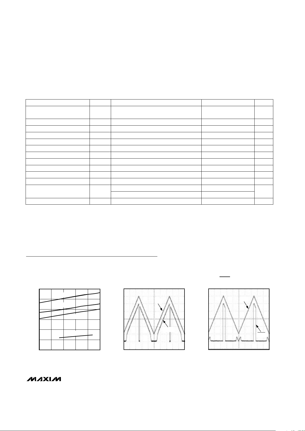
Figure 4 shows typical transient duration vs. reset comparator overdrive, for which the MAX6342–MAX6345 do
not generate a reset pulse. The graph was generated
using a negative-going pulse applied to VCC, starting
0.5V above the actual reset threshold and ending below
it by the magnitude indicated (reset comparator overdrive). The graph indicates the maximum pulse width a
negative-going V
CC
transient can have without causing
a reset pulse. As the magnitude of the transient increases (goes further below the reset threshold), the maximum allowable pulse width decreases.
Typically, a VCCtransient that goes 100mV below the
reset threshold and lasts 12µs or less will not cause a
reset pulse. A 1µF bypass capacitor mounted as close
as possible to the VCCpin provides additional transient
immunity.
Ensuring a Valid Reset Output
Down to V
CC
= 0
The MAX6342–MAX6345 are guaranteed to operate
properly down to VCC= +1V. In applications that require
valid reset levels down to VCC= 0, a pull-down resistor
to active-low outputs (MAX6342/MAX6345) and a pull-up
resistor to active-high outputs (MAX6344/MAX6345)
ensure that the reset line is valid when the reset output is
no longer sinking or sourcing current (Figures 5 and 6).
Note that this method does not work with the open-drain
output of the MAX6343. The resistor value used is not
critical, but it must be large enough not to load the reset
6-Pin µP Reset Circuit with
Power-Fail Comparator
6 _______________________________________________________________________________________
MAX6343
V
CC
GND
RESET
RESET
µP
+5.0V
+3.3V
10k
V
CC
160
100
120
140
0
1 100 1000
60
40
20
80
RESET COMPARATOR OVERDRIVE , V
TH
- VCC (mV)
MAXIMUM TRANSIENT DURATION (µs)
10
MAX634_L/M
MAX634_T/S/R/Z
Figure 4. Maximum Transient Duration Magnitude Rejection
Figure 3. Open-Drain RESET Output Allows Use with Multiple
Supplies
V
CC
V
CC
GND
100k
RESET
MAX6342
MAX6345
V
CC
V
CC
GND
100k
RESET
MAX6344
MAX6345
Figure 5. Ensuring RESET Valid to VCC= 0 on Active-Low
Push-Pull Outputs
Figure 6. Ensuring RESET Valid to VCC= 0 on Active-High
Push-Pull Outputs

output when V
CC
is above the reset threshold. For most
applications, 100kΩ is adequate.
Monitoring Two Supplies
Monitor another voltage by connecting a resistor-divider
to PFI as shown in Figure 7. The threshold voltage will
then be given by:
V
TH(PFI)
= 1.25[(R1 + R2) / R2]
where V
TH(PFI)
is the threshold at which the monitored
voltage will trip PFO.
A good rule of thumb for selecting the resistors is to
choose R2 between 250kΩ and 500kΩ and solve for R1.
Connect PFO to MR in applications that require reset to
assert when the second voltage falls below its threshold.
Monitoring a Negative Voltage
Connect the circuit as shown in Figure 8 to use the
power-fail comparator to monitor a negative supply rail.
PFO stays low when V- is good. When V- rises to cause
PFI to be above +1.25V, PFO goes high. By adding the
resistors and transistor as shown, a high PFO triggers
reset. As long as PFO remains high, the MAX6342/
MAX6343/MAX6344 will keep reset asserted. Note that
the accuracy of this circuit depends on the PFI threshold tolerance, the V
CC
line voltage, and the resistors.
Also, ensure that the voltage at PFI remains above
GND.
Interfacing to µPs with
Bidirectional Reset Pins
Use the circuit shown in Figure 9 to interface the
MAX6342 or MAX6345 with a µP with bidirectional reset
pins. The 4.7kΩ resistor between the reset output and
the µP I/O line will ensure that the resets do not cause
an indeterminate logic level.
MAX6342–MAX6345
6-Pin µP Reset Circuit with
Power-Fail Comparator
_______________________________________________________________________________________ 7
V
CC
V
CC
R1
R2
V+
GND
( ) ARE FOR MAX6344 ONLY.
TO µP
PFI MR
PFO
RESET
(RESET)
MAX6342
MAX6343
MAX6344
Figure 7. Monitoring Two Supplies
V
CC
V
CC
R1
R1 R2
R2
V-
GND
( ) ARE FOR MAX6344 ONLY.
V
CC
- 1.25V = 1.25V - V
TRIP
100k
100k
PFI
MR
PFO
RESET
(RESET)
MAX6342
MAX6343
MAX6344
V
TRIP
< 0
Figure 8. Monitoring a Negative Voltage
V
CC
GND
BUFFERED RESET TO
OTHER SYSTEM
COMPONENTS
4.7k
RESET
MAX6342
MAX6345
V
CC
GND
µP
RESET
Figure 9. Interfacing to µPs with Bidirectional Reset I/O
SOT Top Marks
PART
SOT TOP
MARK
PART
SOT TOP
MARK
MAX6342LUT-T AACP MAX6344LUT-T AADQ
MAX6342MUT-T AACQ MAX6344MUT-T AADR
MAX6342TUT-T AACR MAX6344TUT-T AADS
MAX6342SUT-T AACS MAX6344SUT-T AADT
MAX6342RUT-T AACT MAX6344RUT-T AADU
MAX6342ZUT-T AACU MAX6344ZUT-T AADV
MAX6343LUT-T AACV MAX6345LUT-T AADW
MAX6343MUT-T AACW MAX6345MUT-T AADX
MAX6343TUT-T AACX MAX6345TUT-T AADY
MAX6343SUT-T AACY MAX6345SUT-T AADZ
MAX6343RUT-T AACZ MAX6345RUT-T AAEA
MAX6343ZUT-T AADA MAX6345ZUT-T AAEB

MAX6342–MAX6345
6-Pin µP Reset Circuit with
Power-Fail Comparator
Maxim cannot assume responsibility for use of any circuitry other than circuitry entirely embodied in a Maxim product. No circuit patent licenses are
implied. Maxim reserves the right to change the circuitry and specifications without notice at any time.
8
_____________________Maxim Integrated Products, 120 San Gabriel Drive, Sunnyvale, CA 94086 408-737-7600
© 1999 Maxim Integrated Products Printed USA is a registered trademark of Maxim Integrated Products.
V
CC
PFI
MR
PFO
µP
RESET
UNREGULATED DC
PUSHBUTTON
SWITCH
INTERRUPT
MAX6342
LINEAR
REGULATOR
RESET
V
CC
GND
PFI
16
5
V
CC
TOP VIEW
2
34
RESET
RESET
PFO
MAX6345
SOT23-6
Typical Operating Circuit Pin Configurations (continued)
TRANSISTOR COUNT: 403
Chip Information
________________________________________________________Package Information
6LSOT.EPS
 Loading...