

_______________General Description
The MAX6325/MAX6341/MAX6350 are low-noise, precision voltage references with extremely low, 0.5ppm/°C
typical temperature coefficients and excellent, ±0.02%
initial accuracy. These devices feature buried-zener
technology for lowest noise performance. Load-regulation specifications are guaranteed for source and sink
currents up to 15mA. Excellent line and load regulation
and low output impedance at high frequencies make
them ideal for high-resolution data-conversion systems
up to 16 bits.
The MAX6325 is set for a 2.500V output, the MAX6341
is set for a 4.096V output, and the MAX6350 is set for a
5.000V output. All three provide for the option of external trimming and noise reduction.
________________________Applications
High-Resolution Analog-to-Digital
and Digital-to-Analog Converters
High-Accuracy Reference Standard
High-Accuracy Industrial and Process Control
Digital Voltmeters
ATE Equipment
Precision Current Sources
____________________________Features
♦ Ultra-Low, 1ppm/°C Max Tempco
♦ Very Low, 1.5µVp-p Noise (0.1Hz to 10Hz)
(MAX6325)
♦ ±0.02% Initial Accuracy (MAX6350)
♦ ±15mA Output Source and Sink Current
♦ Low, 18mW Power Consumption (MAX6325)
♦ Industry-Standard Pinout
♦ Optional Noise Reduction and Voltage Trim
♦ Excellent Transient Response
♦ 8-Pin SO Package Available
♦ Low, 30ppm/1000h Long-Term Stability
♦ Stable for All Capacitive Loads
MAX6325/MAX6341/MAX6350
1ppm/°C, Low-Noise, +2.5V/+4.096V/+5V
Voltage References
________________________________________________________________
Maxim Integrated Products
1
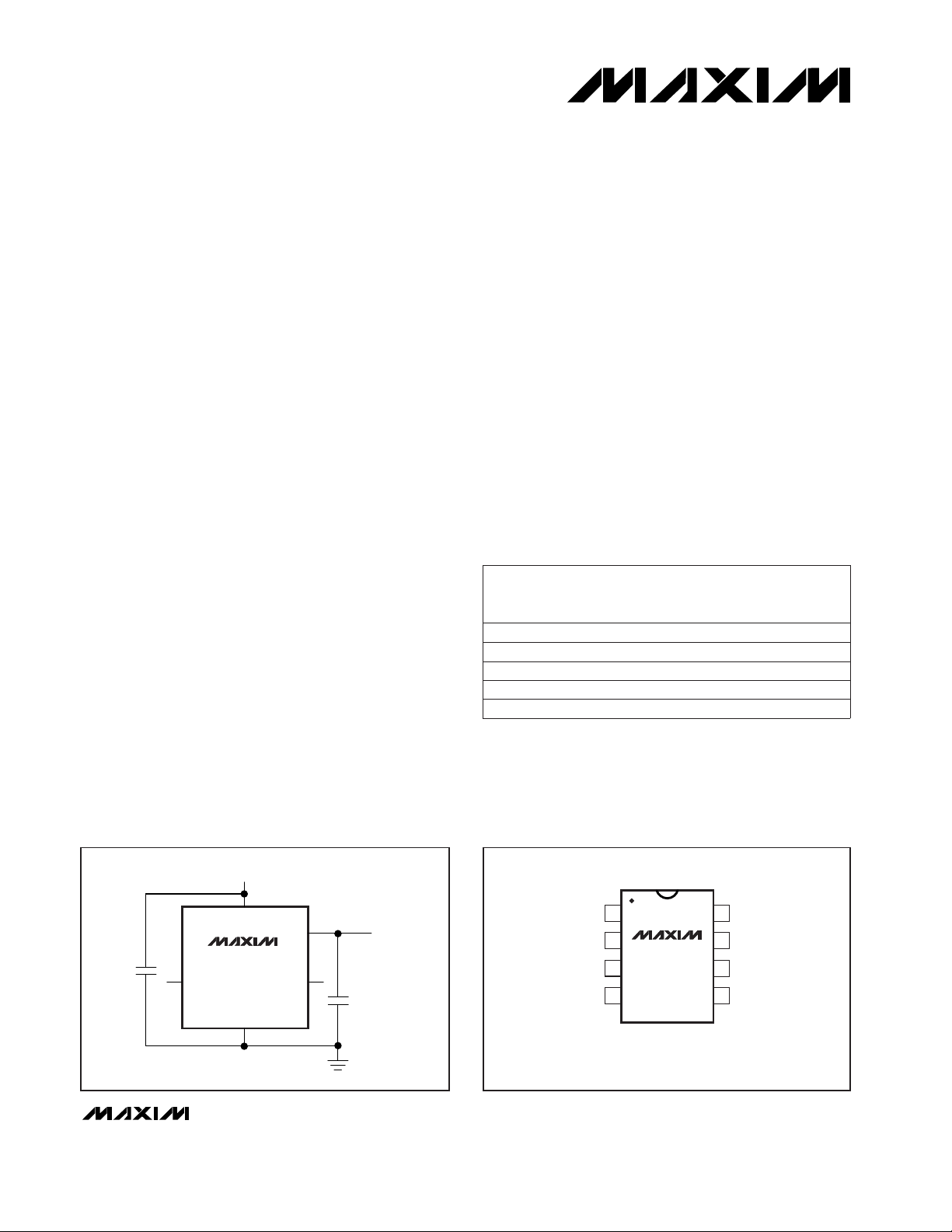
REFERENCE OUT
GND
NR
*OPTIONAL
TRIM
OUT
IN
8V TO 36V INPUT
*
2.2µF
*
2.2µF
MAX6325
MAX6341
MAX6350
__________Typical Operating Circuit
OUT
NR
TRIM
GND
1
2
8
7
I.C.
I.C.
IN
I.C.
MAX6325
MAX6341
MAX6350
DIP/SO
TOP VIEW
I.C. = INTERNALLY CONNECTED; DO NOT USE
3
4
6
5
__________________Pin Configuration
19-1203; Rev 0; 4/97
______________Ordering Information
Ordering Information continued at end of data sheet.
For free samples & the latest literature: http://www.maxim-ic.com, or phone 1-800-998-8800
MAX6325CPA
MAX6325CSA 0°C to +70°C
0°C to +70°C 1.0
1.0
8 Plastic DIP
8 SO
MAX6325EPA -40°C to +85°C 1.58 Plastic DIP
PART TEMP. RANGE
MAX
TEMPCO
(ppm/
°C)
PIN-
PACKAGE
MAX6325ESA -40°C to +85°C 1.58 SO
MAX6325MJA -55°C to +125°C 2.58 CERDIP
MAX6325/MAX6341/MAX6350
1ppm/°C, Low-Noise, +2.5V/+4.096V/+5V
Voltage References
2 _______________________________________________________________________________________
ABSOLUTE MAXIMUM RATINGS
ELECTRICAL CHARACTERISTICS—MAX6325
(VIN= 10V, I
OUT
= 0mA, TA= T
MIN
to T
MAX
, unless otherwise noted. Typical values are at TA= +25°C.)
Stresses beyond those listed under “Absolute Maximum Ratings” may cause permanent damage to the device. These are stress ratings only, and functional
operation of the device at these or any other conditions beyond those indicated in the operational sections of the specifications is not implied. Exposure to
absolute maximum rating conditions for extended periods may affect device reliability.
(Voltages Referenced to GND)
IN................................................................................-0.3V to 40V
OUT, TRIM..................................................................-0.3V to 12V
NR.................................................................................-0.3V to 6V
OUT Short Circuit to GND Duration (V
IN
≤ 12V)..........Continuous
OUT Short Circuit to GND Duration (V
IN
≤ 40V) ....................5sec
OUT Short Circuit to IN Duration (V
IN
≤ 12V) ..............Continuous
Continuous Power Dissipation (T
A
= +70°C)
Plastic DIP (derate 9.09mW/°C above +70°C)................727mW
SO (derate 5.88mW/°C above +70°C)............................471mW
CERDIP (derate 8.00mW/°C above +70°C)....................640mW
Operating Temperature Ranges
MAX63_ _ C_ A.......................................................0°C to +70°C
MAX63_ _ E_ A....................................................-40°C to +85°C
MAX63_ _ MJA..................................................-55°C to +125°C
Storage Temperature Range ..............................-65°C to +150°C
Lead Temperature (soldering, 10sec)...............................+300°C
Load Regulation (Note 2)
∆V
OUT
/
∆I
OUT
ppm/mA
+25°C
+25°C
µs5+25°Ct
ON
Turn-On Settling Time To ±0.01% of final value
µV
RMS
1.3 2.8+25°C
e
n
Output Noise Voltage (Note 3)
µVp-p1.5
mV±15 ±25C, E, M∆V
OUT
Trim-Adjustment Range
mA
3.0C, E, M
I
IN
Supply Current
1.8 2.7+25°C
10 30M
1 7
10Hz ≤ f ≤ 1kHz
E
0.1Hz ≤ f ≤ 10Hz
Figure 1
1 6C
ppm/
1000h
3 15M
30+25°C
1 7
∆V
OUT
/ tLong-Term Stability
E
1 6C
+25°CTemperature Hysteresis ppm20(Note 4)
10M
8E
7C
2 5+25°C
10V ≤ VIN≤ 36V
45M
35E
30C
MAX6325MJA 1.0 2.5M
8V ≤ VIN≤ 10V
CONDITIONS
MAX6325E_A
MAX6325C_A
MAX6325
ppm/V
10 18+25°C
∆V
OUT
/
∆
V
IN
Line Regulation (Note 2)
ppm/°C0.75 1.5ETCV
OUT
Output Voltage Temperature
Coefficient (Note 1)
0.5 1.0C
Output Voltage V
OUT
2.499 2.500 2.501 V
T
A
C, E, M
PARAMETER SYMBOL MIN TYP MAX UNITS
Input Voltage Range V
IN
8 36 V
Sourcing: 0mA ≤ I
OUT
≤ 15mA
Sinking: -15mA ≤ I
OUT
≤ 0mA
MAX6325/MAX6341/MAX6350
1ppm/°C, Low-Noise, +2.5V/+4.096V/+5V
Voltage References
_______________________________________________________________________________________ 3
(Note 4)
V4.095 4.096 4.097V
OUT
Output Voltage +25°C
20 ppmTemperature Hysteresis
C 0.5 1.0
MAX6341
Output Voltage Temperature
Coefficient (Note 1)
TCV
OUT
E 0.75 1.5
ppm/°C
+25°C
+25°C 10 18
MAX6341C_A
MAX6341E_A
CONDITIONS
30
ppm/
1000h
8V ≤ VIN≤ 10V
Long-Term Stability ∆V
OUT
/ t +25°C
Line Regulation (Note 2)
∆V
OUT
/
∆V
IN
ppm/V
Figure 1
0.1Hz ≤ f ≤ 10Hz
10Hz ≤ f ≤ 1kHz
V8 36V
IN
Input Voltage Range
+25°C 1.9 2.9
I
IN
C, E, M 3.2
mA
Trim-Adjustment Range
UNITSMIN TYP MAXSYMBOLPARAMETER
∆V
OUT
C, E, M ±24 ±40 mV
2.4 µVp-p
Output Noise Voltage (Note 3) e
n
+25°C
2.0 4.0 µV
RMS
C, E, M
T
A
ELECTRICAL CHARACTERISTICS—MAX6341
(VIN= 10V, I
OUT
= 0mA, TA= T
MIN
to T
MAX
, unless otherwise noted. Typical values are at TA= +25°C.)
M 1.0 2.5MAX6341MJA
To ±0.01% of final valueTurn-On Settling Time t
ON
+25°C 8 µs
C 30
E 35
M 45
+25°C 2 5
10V ≤ VIN≤ 36V
C 7
E 8
M 10
Supply Current
C 1 6
E 1 7
M 3 9
C 1 6
E 1 7
M 7 18
+25°C
Sourcing: 0mA ≤ I
OUT
≤ 15mA
Sinking: -15mA ≤ I
OUT
≤ 0mA
∆V
OUT
/
∆I
OUT
Load Regulation (Note 2) ppm/mA
MAX6325/MAX6341/MAX6350
1ppm/°C, Low-Noise, +2.5V/+4.096V/+5V
Voltage References
4 _______________________________________________________________________________________
ELECTRICAL CHARACTERISTICS—MAX6350
(VIN= 10V, I
OUT
= 0mA, TA= T
MIN
to T
MAX
, unless otherwise noted. Typical values are at TA= +25°C.)
(Note 4)
V4.999 5.000 5.001V
OUT
Output Voltage +25°C
20 ppmTemperature Hysteresis
C 0.5 1.0
MAX6350
E 0.75 1.5
+25°C
+25°C 10 18
MAX6350C_A
MAX6350E_A
CONDITIONS
30
ppm/
1000h
8V ≤ VIN≤ 10V
Long-Term Stability ∆V
OUT
/ t +25°C
Line Regulation (Note 2)
∆V
OUT
/
∆V
IN
ppm/V
Figure 1
To ±0.01% of final value
V8 36V
IN
Input Voltage Range
+25°C 2.0 3.0
Supply Current I
IN
C, E, M 3.3
mA
Trim-Adjustment Range
UNITSMIN TYP MAXSYMBOLPARAMETER
∆V
OUT
C, E, M ±30 ±50 mV
10 µsTurn-On Settling Time t
on
+25°C
C, E, M
T
A
C 30
E 35
M 45
C 7
+25°C 2 5
E 8
10V ≤ VIN≤ 36V
M 10
C 1 6
C 1 6
E 1 7
E 1 7
M
M 2 9
6 15
0.1Hz ≤ f ≤ 10Hz
10Hz ≤ f ≤ 1kHz
3.0 µVp-p
Output Noise Voltage (Note 3) e
n
+25°C
2.5 5.0 µV
RMS
Output Voltage Temperature
Coefficient (Note 1)
TCV
OUT
ppm/°C
M 1.0 2.5MAX6350MJA
Note 1: Temperature coefficient is measured by the box method; i.e., the maximum ∆V
OUT
is divided by ∆T x V
OUT
.
Note 2: Line regulation (∆V
OUT
/ (V
OUT
x ∆
VIN
)) and load regulation (∆V
OUT
/ (V
OUT
x ∆I
OUT
)) are measured with pulses and do not
include output voltage changes due to die-temperature changes.
Note 3: Noise specifications are 100% tested for the 10Hz to 1kHz bandwidth. Production testing in the 0.1Hz to 10Hz bandwidth is
available upon request.
Note 4: Temperature hysteresis is specified at T
A
= +25°C by measuring V
OUT
before and after changing temperature by +25°C
using the plastic DIP package.
+25°C
Sourcing: 0mA ≤ I
OUT
≤ 15mA
Sinking: -15mA ≤ I
OUT
≤ 0mA
ppm/mA
∆V
OUT
/
∆I
OUT
Load Regulation (Note 2)

MAX6325/MAX6341/MAX6350
1ppm/°C, Low-Noise, +2.5V/+4.096V/+5V
Voltage References
_______________________________________________________________________________________
5
__________________________________________Typical Operating Characteristics
(VIN= 10V, I
OUT
= 0mA, TA = +25°C, unless otherwise noted.)
2.0
-1.5
-55 -15 65
MAX6350
NORMALIZED OUTPUT VOLTAGE
vs. TEMPERATURE
-1.0
1.0
MAX6325 -01
TEMPERATURE (°C)
∆V
OUT
(mV)
∆V
OUT
(ppm)
25 105-35 5 8545 125
0.5
0
-0.5
1.5
400
-300
-200
200
100
0
-100
300
-20
-10
0
10
20
30
40
50
60
0 5 10 15 20 25 30 35 40
CHANGE IN OUTPUT VOLTAGE
vs. INPUT VOLTAGE
MAX6325-04
V
IN
(V)
∆V
OUT
(ppm)
-55 -15 65
MAX6341
NORMALIZED OUTPUT VOLTAGE
vs. TEMPERATURE
-1.0
1.0
MAX6325 -02
TEMPERATURE (°C)
∆V
OUT
(mV)
∆V
OUT
(ppm)
25 105-35 5 8545 125
0.5
0
-0.5
1.5
-250
-125
0
125
250
375
-0.4
-0.3
-0.2
-0.1
0 0
0.1
0.2
0.3
0.4
0.5
0.6
0.7
-160
-120
-80
-40
40
80
120
160
200
240
280
-55 -15 65
MAX6325
NORMALIZED OUTPUT VOLTAGE
vs. TEMPERATURE
MAX6325 03
TEMPERATURE (°C)
∆V
OUT
(mV)
∆V
OUT
(ppm)
25 105-35 5 8545 125
-250
-200
-150
-100
-50
0
50
100
150
200
-40 -30 -20 -10 0 10 20 30 40
MAX6325
CHANGE IN OUTPUT VOLTAGE
vs. OUTPUT CURRENT
MAX6325-05
I
OUT
(mA)
∆V
OUT
(µV)
TA = +85°C
TA = -40°C
TA = +25°C
-300
-200
-100
0
100
200
300
-40 -30 -20 -10 0 10 20 30 40
MAX6341
CHANGE IN OUTPUT VOLTAGE
vs. OUTPUT CURRENT
MAX6325-06
I
OUT
(mA)
∆V
OUT
(µV)
TA = +25°C
T
A
= -40°C
T
A
= +85°C
-400
-300
-200
-100
0
100
200
300
-40 -30 -20 -10 0 10 20 30 40
MAX6350
CHANGE IN OUTPUT VOLTAGE
vs. OUTPUT CURRENT
MAX6325-07
I
OUT
(mA)
∆V
OUT
(µV)
TA = +25°C
TA = -40°C
TA = +85°C
1.0
1.2
1.4
1.6
1.8
2.0
2.2
2.4
2.6
2.8
3.0
0 5 10 15 20 25 30 35 40
SUPPLY CURRENT vs. SUPPLY VOLTAGE
MAX6325-08
SUPPLY VOLTAGE (V)
SUPPLY CURRENT (mA)
MAX6325
MAX6341
MAX6350
1.0
1.5
2.0
2.5
3.0
3.5
-55 -35 -15 5 25 45 65 85 105 125
SUPPLY CURRENT vs. TEMPERATURE
MAX6325-09
TEMPERATURE (°C)
SUPPLY CURRENT (mA)
MAX6341
MAX6350
MAX6325

MAX6325/MAX6341/MAX6350
1ppm/°C, Low-Noise, +2.5V/+4.096V/+5V
Voltage References
6 _______________________________________________________________________________________
MAX6341
0.1Hz to 10Hz NOISE
V
OUT
, 1µV/div
MAX6325-16
1sec/div
C
OUT
= CNR = 0µF
0
5
10
15
20
25
30
35
40
45
50
10 100 1k 10k
MAX6325
OUTPUT NOISE-VOLTAGE
DENSITY vs. FREQUENCY
MAX6325-10
FREQUENCY (Hz)
CNR = 0µF
CNR = 1µF
OUTPUT NOISE DENSITY (nV/√ Hz)
MAX6325
0.1Hz to 10Hz NOISE
V
OUT
, 0.5µV/div
MAX6325-17
1sec/div
C
OUT
= CNR = 0µF
0
10
20
30
40
50
60
70
80
90
10 100 1k 10k
MAX6341
OUTPUT NOISE-VOLTAGE
DENSITY vs. FREQUENCY
MAX6325-11
FREQUENCY (Hz)
CNR = 0µF
CNR = 1µF
OUTPUT NOISE DENSITY (nV/√ Hz)
0
10
20
30
40
50
60
70
80
100
90
10 100 1k 10k
MAX6350
OUTPUT NOISE-VOLTAGE
DENSITY vs. FREQUENCY
MAX6325-12
FREQUENCY (Hz)
CNR = 0µF
CNR = 1µF
OUTPUT NOISE DENSITY (nV/√ Hz)
MAX6350
0.1Hz to 10Hz NOISE
V
OUT
, 1µV/div
1sec/div
MAX6325-18
C
OUT
= CNR = 0µF
10 1M10k
FREQUENCY (Hz)
100 1k 100k
100
0.01
OUTPUT IMPEDANCE vs. FREQUENCY
0.1
MAX6325-13
OUTPUT IMPEDANCE (Ω)
1
10
I
SINK
= 5mA
I
SOURCE
= 5mA
60
70
80
90
100
110
120
10 100 1k 10k
RIPPLE REJECTION
vs. FREQUENCY (C
NR
= 1µF)
MAX6325-14
FREQUENCY (Hz)
RIPPLE REJECTION (dB)
MAX6341
MAX6325
MAX6350
60
65
70
75
80
85
90
95
10 100 1k 10k
RIPPLE REJECTION
vs. FREQUENCY (C
NR
= 0µF)
MAX6325-15
FREQUENCY (Hz)
RIPPLE REJECTION (dB)
MAX6325
MAX6341
MAX6350
____________________________Typical Operating Characteristics (continued)
(VIN= 10V, I
OUT
= 0mA, TA = +25°C, unless otherwise noted.)

MAX6325/MAX6341/MAX6350
1ppm/°C, Low-Noise, +2.5V/+4.096V/+5V
Voltage References
_______________________________________________________________________________________
7
2µs/div
LOAD-TRANSIENT RESPONSE (SOURCING)
B
A
A: I
OUT
, 10mA/div (SOURCING)
B: V
OUT
, 500µV/div
MAX6325-19
0mA
-10mA
2µs/div
LOAD-TRANSIENT RESPONSE (SINKING)
B
A
0mA
10mA
A: I
OUT
, 10mA/div (SINKING)
B: V
OUT
, 500µV/div
MAX6325-20
____________________________Typical Operating Characteristics (continued)
(VIN= 10V, I
OUT
= 0mA, T
A
= +25°C, unless otherwise noted.)
1µs/div
LOAD-TRANSIENT RESPONSE
B
A
A: I
OUT
(±10mA SOURCE AND SINK), 20mA/div, AC COUPLED
B: V
OUT
, 20mV/div, AC COUPLED
MAX6325-21
+10mA
-10mA
VIN = 10V
C
OUT
= CNR = 0µF
1µs/div
MAX6341
TURN-ON AND TURN-OFF TRANSIENT RESPONSE
B
A
A: VIN, 10V/div
B: V
OUT
, 1V/div
MAX6325-25
+10V
0V
CIN = C
OUT
= CNR = 0µF
1µs/div
MAX6325
TURN-ON AND TURN-OFF TRANSIENT RESPONSE
B
A
A: VIN, 10V/div
B: V
OUT
, 1V/div
MAX6325-26
+10V
0V
CIN = C
OUT
= CNR = 0µF
1µs/div
MAX6350
TURN-ON AND TURN-OFF TRANSIENT RESPONSE
B
A
A: VIN, 10V/div
B: V
OUT
, 1V/div
MAX6325-27
+10V
0V
CIN = C
OUT
= CNR = 0µF

MAX6325/MAX6341/MAX6350
1ppm/°C, Low-Noise, +2.5V/+4.096V/+5V
Voltage References
8 _______________________________________________________________________________________
_______________Detailed Description
Temperature Stability
The MAX6325/MAX6341/MAX6350 are highly stable,
low-noise voltage references that use a low-power temperature-compensation scheme to achieve laboratorystandard temperature stability. This produces a nearly
flat temperature curve, yet does not require the power
associated with heated references.
The output voltage can be trimmed a minimum of 0.6%
by connecting a 10kΩ potentiometer between OUT and
GND, and connecting its tap to the TRIM pin, as shown
in Figure 1. The external trimming does not affect temperature stability.
Noise Reduction
To augment wideband noise reduction, add a 1µF
capacitor to the NR pin (Figure 2). Larger values do not
improve noise appreciably (see
Typical Operating
Characteristics
).
Noise in the power-supply input can affect output
noise, but can be reduced by adding an optional
bypass capacitor to the IN pin and GND.
Bypassing
The MAX6325/MAX6341/MAX6350 are stable with
capacitive load values from 0µF to 100µF, for all values
of load current. Adding an output bypass capacitor can
help reduce noise and output glitching caused by load
transients.
__________Applications Information
Negative Regulator
Figure 3 shows how both a +5V and -5V precision reference can be obtained from a single, unregulated +5V
supply. A MAX681 generates approximately ±9V to
operate the MAX6350 reference and MAX400 inverting
amplifier. The +5V is inverted by the ultra-low offset
MAX400 op amp. Resistor R1 is optional, and may be
used to trim the ±5V references. R2 and R4 should be
matched, both in absolute resistance and temperature
coefficient. R3 is optional, and is adjusted to set the -5V
reference.
_____________________Pin Description
NAME FUNCTION
1, 7, 8 I.C.
Internally Connected. Do not use.
2 IN Positive Power-Supply Input
PIN
4 GND Ground
3 NR
Noise Reduction. Optional capacitor
connection for wideband noise
reduction. Leave open if not used
(Figure 2).
6 OUT Voltage Reference Output
5 TRIM
External Trim Input. Allows ±1%
output adjustment (Figure 1).
Leave open if not used.
Figure 1. Output Voltage Adjustment Figure 2. Noise-Reduction Capacitor
NR
8V TO 36V INPUT
IN
MAX6325
MAX6341
MAX6350
GND
8V TO 36V INPUT
IN
MAX6325
MAX6341
NR
MAX6350
GND
OUT
TRIM
REFERENCE OUT
*
10k
1µF
*OPTIONAL
OUT
TRIM
REFERENCE OUT

MAX6325/MAX6341/MAX6350
1ppm/°C, Low-Noise, +2.5V/+4.096V/+5V
Voltage References
_______________________________________________________________________________________ 9
MAX6350
MAX865
IN
VCCV+
V-
GND
C2-
C2+
C1-
C1+
+5V INPUT
+REFERENCE OUT
-REFERENCE OUT
OUT
TRIM
10k
R1
100k
R4
R2
100k
R3
1k
NR
2.2µF
C1
3.3µF
3.3µF
2.2µF
C2
1µF
2.2µF
0.1µF
0.1µF
C3
1µF
C4
GND
MAX400
Figure 3. +5V and -5V References from a Single +5V Supply
_Ordering Information (continued)
___________________Chip Information
TRANSISTOR COUNT: 435
MAX6341CPA
MAX6341CSA 0°C to +70°C
0°C to +70°C 1.0
1.0
8 Plastic DIP
8 SO
MAX6341EPA -40°C to +85°C 1.58 Plastic DIP
PART TEMP. RANGE
MAX.
TEMPCO
(ppm/°C)
PIN-
PACKAGE
MAX6350ESA -40°C to +85°C 1.58 SO
MAX6350MJA -55°C to +125°C 2.58 CERDIP
MAX6341ESA -40°C to +85°C 1.58 SO
MAX6341MJA -55°C to +125°C 2.58 CERDIP
MAX6350CPA
0°C to +70°C 1.08 Plastic DIP
MAX6350CSA 0°C to +70°C 1.08 SO
MAX6350EPA -40°C to +85°C 1.58 Plastic DIP

MAX6325/MAX6341/MAX6350
1ppm/°C, Low-Noise, +2.5V/+4.096V/+5V
Voltage References
10 ______________________________________________________________________________________
________________________________________________________Package Information
PDIPN.EPS
SOICN.EPS

MAX6325/MAX6341/MAX6350
1ppm/°C, Low-Noise, +2.5V/+4.096V/+5V
Voltage References
______________________________________________________________________________________ 11
CDIPS.EPS
___________________________________________Package Information (continued)

Maxim cannot assume responsibility for use of any circuitry other than circuitry entirely embodied in a Maxim product. No circuit patent licenses are
implied. Maxim reserves the right to change the circuitry and specifications without notice at any time.
12
__________________Maxim Integrated Products, 120 San Gabriel Drive, Sunnyvale, CA 94086 (408) 737-7600
© 1997 Maxim Integrated Products Printed USA is a registered trademark of Maxim Integrated Products.
MAX6325/MAX6341/MAX6350
1ppm/°C, Low-Noise, +2.5V/+4.096V/+5V
Voltage References
NOTES
 Loading...