

Maxim MAX6337US24D3-T, MAX6337US25D1-T, MAX6337US25D2-T, MAX6337US24D1-T, MAX6337US23D2-T Datasheet
...
For free samples & the latest literature: http://www.maxim-ic.com, or phone 1-800-998-8800.
For small orders, phone 1-800-835-8769.
General Description
The MAX6335/MAX6336/MAX6337 microprocessor (µP)
supervisory circuits monitor the power supplies in 1.8V
to 3.3V µP and digital systems. They increase circuit reliability and reduce cost by eliminating external components and adjustments. They also feature a debounced
manual-reset input.
These devices perform a single function: they assert a
reset signal whenever the VCCsupply voltage declines
below a preset threshold or whenever manual reset is
asserted. Reset remains asserted for a preset timeout
period after VCChas risen above the reset threshold or
after manual reset is deasserted. The only difference
among the three devices is their output. The MAX6336
(push/pull) and MAX6337 (open-drain) have an activelow RESET output, while the MAX6335 (push/pull) has
an active-high RESET output. The MAX6335/MAX6336
are guaranteed to be in the correct state for VCCdown
to 0.7V. The MAX6337 is guaranteed to be in the correct state for VCCdown to 1.0V.
The reset comparator in these ICs is designed to ignore
fast transients on VCC. Reset thresholds are factorytrimmable between 1.6V and 2.5V, in approximately
100mV increments. There are 15 standard versions
available (2500 piece minimum-order quantity); contact
the factory for availability of nonstandard versions
(10,000 piece minimum-order quantity). For space-critical applications, the MAX6335/MAX6336/MAX6337
come packaged in a 4-pin SOT143.
Applications
Pentium II™ Computers
Computers
Controllers
Intelligent Instruments
Critical µP/µC Power Monitoring
Portable/Battery-Powered Equipment
Automotive
Features
♦ Ultra-Low 0.7V Operating Supply Voltage
♦ Low 3.3µA Supply Current
♦ Precision Monitoring of 1.8V and 2.5V Power-
Supply Voltages
♦ Reset Thresholds Available from 1.6V to 2.5V,
in Approximately 100mV Increments
♦ Debounced Manual Reset
♦ Fully Specified over Temperature
♦ Three Power-On Reset Pulse Widths Available
(1ms min, 20ms min, 100ms min)
♦ Low Cost
♦ Three Available Output Structures: Push/Pull
RESET, Push/Pull RESET, Open-Drain RESET
♦ Guaranteed RESET/RESET Valid to V
CC
= 0.7V
(MAX6335/MAX6336)
♦ Power-Supply Transient Immunity
♦ No External Components
♦ 4-Pin SOT143 Package
♦ Pin-Compatible with MAX811/MAX812 and
MAX6314/MAX6315
MAX6335/MAX6336/MAX6337
4-Pin, Ultra-Low-Voltage, Low-Power
µP Reset Circuits with Manual Reset
________________________________________________________________
Maxim Integrated Products
1
19-1412; Rev 0; 12/98
PART*
MAX6335US__D_-T
MAX6336US__D_-T
MAX6337US__D_-T
-40°C to +85°C
-40°C to +85°C
-40°C to +85°C
TEMP. RANGE PIN-PACKAGE
4 SOT143
4 SOT143
4 SOT143
Ordering Information
*
These devices are available in factory-set VCCreset thresholds from 1.6V to 2.5V, in approximately 0.1V increments.
Choose the desired reset threshold suffix from Table 1 and
insert it in the blanks following “US” in the part number.
Factory-programmed reset timeout periods are also available.
Insert the number corresponding to the desired nominal reset
timeout period (1 = 1ms min, 2 = 20ms min, 3 = 100ms min) in
the blank following “D” in the part number. There are 15 standard versions with a required order increment of 2500 pieces.
Sample stock is generally held on the standard versions only
(see Selector Guide). Contact the factory for availability of nonstandard versions (required order increment is 10,000 pieces).
All devices available in tape-and-reel only.
Typical Operating Circuit and Pin Configuration appear
at end of data sheet.
Selector Guide appears at end of data sheet.
Pentium II is a trademark of Intel Corp.
MAX6335/MAX6336/MAX6337
4-Pin, Ultra-Low-Voltage, Low-Power
µP Reset Circuits with Manual Reset
2 _______________________________________________________________________________________
ABSOLUTE MAXIMUM RATINGS
ELECTRICAL CHARACTERISTICS
(VCC= full range, MR = VCCor unconnected, TA= -40°C to +85°C, unless otherwise noted. Typical values are at TA= +25°C and
V
CC
= 3V, reset not asserted.)
Stresses beyond those listed under “Absolute Maximum Ratings” may cause permanent damage to the device. These are stress ratings only, and functional
operation of the device at these or any other conditions beyond those indicated in the operational sections of the specifications is not implied. Exposure to
absolute maximum rating conditions for extended periods may affect device reliability.
Terminal Voltage (with respect to GND)
VCC......................................................................-0.3V to +6V
Push/Pull RESET or RESET, MR ............-0.3V to (V
CC
+ 0.3V)
Open-Drain RESET ..............................................-0.3V to +6V
Input Current (V
CC
).............................................................20mA
Output Current (RESET, RESET).........................................20mA
Rate of Rise, V
CC
............................................................100V/µs
Continuous Power Dissipation (T
A
= +70°C)
SOT143 (derate 4mW/°C above +70°C) .....................320mW
Operating Temperature Range ...........................-40°C to +85°C
Storage Temperature Range.............................-65°C to +160°C
Lead Temperature (soldering, 10sec).............................+300°C
PARAMETER SYMBOL CONDITIONS MIN TYP MAX UNITS
Supply Voltage Range V
CC
TA = 0°C to +85°C
MAX6335/MAX6336 0.7 5.5
MAX6337 1.0 5.5
TA = -40°C to +85°C
MAX6335/MAX6336 0.78 5.5
MAX6337 1.2 5.5
V
Supply Current I
CC
No load
V
CC
= 1.8V
3.0 6.0
V
CC
= 2.5V
3.3 7.0
µA
TA = +25°C
V
TH -
V
TH
V
TH +
1.8% 1.8%
TA = -40°C to +85°C
V
TH -
V
TH
V
TH +
3% 3%
Reset Threshold V
TH
MAX633_US__D_-T,
Table 1
V
VCCFalling Reset Delay VCCfalling at 10V/ms 24
µs
MAX633_US__D1-T 1 1.5 2
MAX633_US__D2-T 20 30 40Reset Active Timeout Period
t
RP
MAX633_US__D3-T 100 150 200
ms
RESET Output Low Voltage
(MAX6336/MAX6337)
V
OL
I
SINK
= 50µA, V
CC
≥ 1.0V 0.4
Reset
asserted
V
RESET Output High Voltage
(MAX6336)
V
OH
I
SOURCE
= 200µA, V
CC
≥ 1.8V 0.8V
CC
I
SOURCE
= 500µA, V
CC
≥ 2.7V 0.8V
CC
V
RESET Output Voltage
(MAX6335)
V
OH
Reset
asserted
I
SOURCE
= 1µA, V
CC
≥ 1.0V 0.8V
CC
I
SOURCE
= 200µA, V
CC
≥ 1.8V 0.8V
CC
V
V
OL
Reset not
asserted
I
SINK
= 500µA, V
CC
≥ 1.8V
I
SINK
= 1.2mA, V
CC
≥ 2.7V
0.3
V
0.3
Reset not
asserted
0.3V
CC
0.7V
CC
MR Minimum Pulse Width
1
V
CC
= 2.6V 160
µs
V
CC
= 2.6V 0.42 µs
V
ns
V
MR
MR Threshold
MR Reset Delay
MR Glitch Immunity
12 20 30 kΩ
MR Pull-Up Resistance
I
SINK
= 500µA, V
CC
≥ 1.8V 0.3
0.5
VCC> VTH, RESET deasserted
µA
RESET Output Leakage
Current (MAX6337)
4-Pin, Ultra-Low-Voltage, Low-Power
µP Reset Circuits with Manual Reset
_______________________________________________________________________________________
3
2.0
2.6
2.2
3.0
3.6
3.8
3.4
3.2
4.0
-60
2.4
-40 -20 0
2.8
20 40 60 80 100
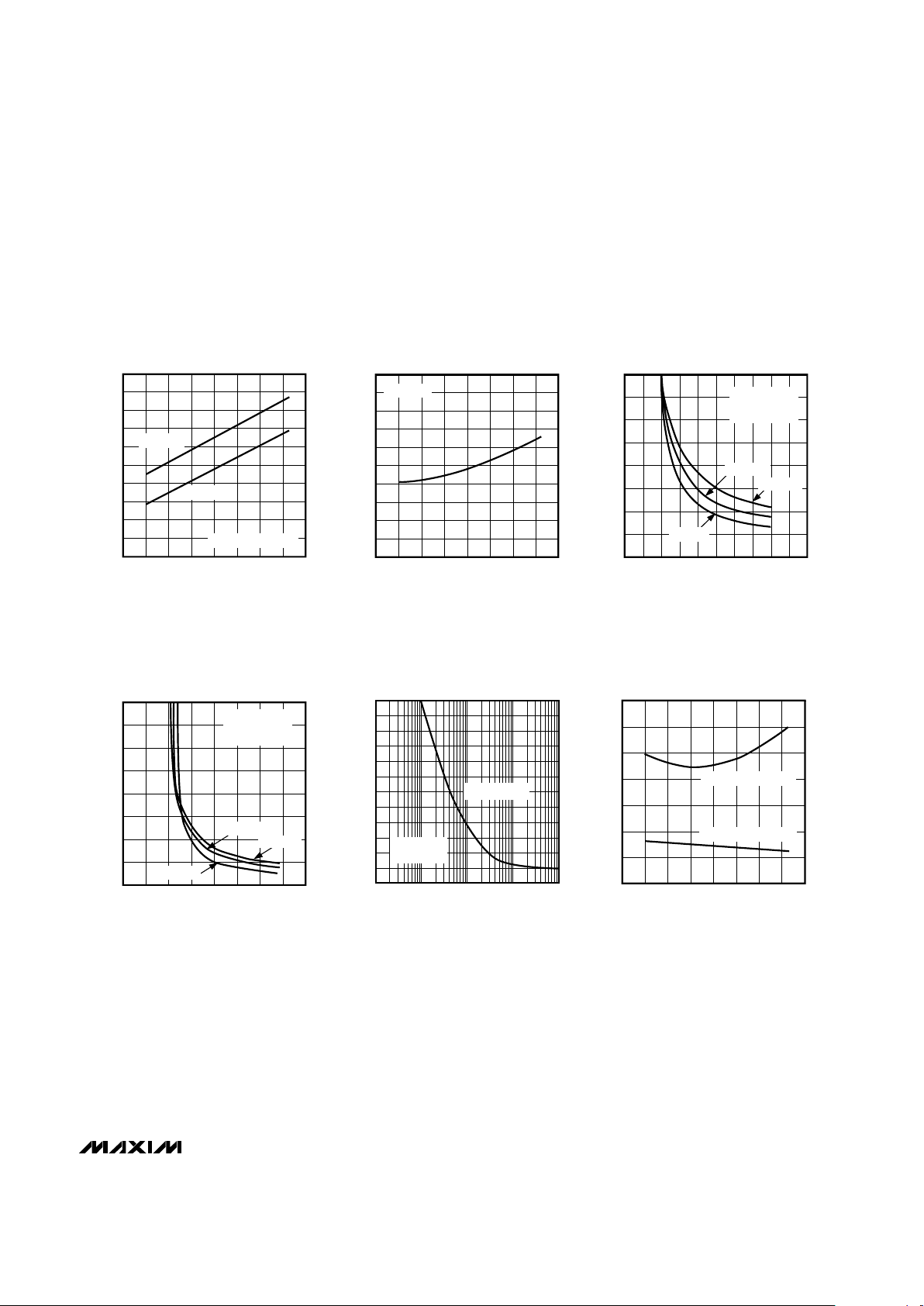
SUPPLY CURRENT vs. TEMPERATURE
MAX6335/36/37 toc-1
TEMPERATURE (°C)
I
CC
(µA)
RESET NOT ASSERTED
VCC = 2.5V
VCC = 1.8V
0.950
0.990
0.970
1.000
1.030
1.040
1.020
1.010
1.050
-60 -40
0.980
-20 0
0.960
20 40 60 80 100
NORMALIZED RESET TIMEOUT PERIOD
vs. TEMPERATURE
MAX6335/36/37-2
TEMPERATURE (°C)
NORMALIZED RESET TIMEOUT PERIOD
V
TH
= 2.2V
0
20
10
30
60
70
50
40
80
0.50 1.00 1.50 2.00 2.50 3.00
OUTPUT VOLTAGE LOW
vs. SUPPLY VOLTAGE
MAX6335/36/37 toc-3
VCC (V)
OUTPUT VOLTAGE LOW (mV)
VTH = 2.5V
I
SINK
= 500µA
RESET ASSERTED
TA = +25°C
TA = +85°C
TA = -40°C
0
40
20
80
60
100
120
140
160
0.5 1.0 1.250.75 1.5 1.75 2.0 2.25 2.5
OUTPUT VOLTAGE HIGH
vs. SUPPLY VOLTAGE
MAX6335/36/37 toc-4
VCC (V)
OUTPUT VOLTAGE HIGH (V
CC
- V
OH
) (mV)
VTH = 2.2V
I
SOURCE = 100µA
RESET ASSERTED
TA = +25°C
TA = +85°C
TA = -40°C
100 1000
0
100
200
400
300
500
600
0.1 1 10
MAXIMUM TRANSIENT DURATION
vs. RESET COMPARATOR OVERDRIVE
MAX6335/36/37 toc-5
RESET COMPARATOR OVERDRIVE (mV)
MAXIMUM TRANSIENT DURATION (µs)
RESET OCCURS
RESET DOES
NOT OCCUR
10
20
-20
40
30
70
60
50
80
-60 0-40 20 40 60 80 100
VCC FALLING PROPAGATION DELAY
vs. TEMPERATURE
MAX6332/33/34 toc-6
TEMPERATURE (°C)
PROPAGATION DELAY (µs)
VCC FALLING AT 10V/ms
VCC FALLING AT 1V/ms
__________________________________________Typical Operating Characteristics
(Reset not asserted, TA= +25°C, unless otherwise noted.)
MAX6335/MAX6336/MAX6337

MAX6335/MAX6336/MAX6337
4-Pin, Ultra-Low-Voltage, Low-Power
µP Reset Circuits with Manual Reset
4 _______________________________________________________________________________________
Pin Description
GND Ground1
—
RESET
Active-Low Reset Output. RESET remains low while VCCis below the reset
threshold, or MR is asserted and for a reset timeout period (t
RP
) after V
CC
rises above the reset threshold, or MR is deasserted. RESET on the
MAX6337 is open-drain.
2 RESET
Active-High Reset Output. RESET remains high while VCCis below the
reset threshold, or MR is asserted and for a reset timeout period (t
RP
) after
V
CC
rises above the reset threshold, or MR is deasserted. RESET also
asserts when MR is low.
NAME FUNCTION
MAX6335
MAX6336
MAX6337
1
2
—
PIN
Applications Information
Manual-Reset Inputs
Many µP-based products require manual-reset capability, allowing the operator, a test technician, or external
logic circuitry to initiate a reset. A logic low on MR
asserts reset. Reset remains asserted while MR is low,
and for the reset active timeout period after MR returns
high. MR has an internal 20kΩ pull-up resistor, so it can
be left unconnected if not used. Connect a normally
open momentary switch from MR to GND to create a
manual-reset function; external debounce circuitry is
not required.
Interfacing to µPs with
Bidirectional Reset Pins
Since the RESET output on the MAX6337 is open-drain,
this device interfaces easily with µPs that have bidirectional reset pins, such as the Motorola 68HC11.
Connecting the µP supervisor’s RESET output directly
to the microcontroller’s (µC’s) RESET pin with a single
pull-up resistor allows either device to assert reset
(Figure 1).
Negative-Going VCCTransients
In addition to issuing a reset to the µP during power-up,
power-down, and brownout conditions, these devices
are relatively immune to short-duration, negative-going
VCCtransients (glitches). The
Typical Operating
Characteristics
show the Maximum Transient Duration
vs. Reset Comparator Overdrive graph. The graph
shows the maximum pulse width that a negative-going
VCCtransient may typically have without issuing a reset
signal. As the amplitude of the transient increases, the
maximum allowable pulse width decreases.
Ensuring a Valid Reset Output
down to V
CC
= 0
When VCCfalls below 1V and approaches the minimum
operating voltage of 0.7V, push/pull-structured reset
sinking (or sourcing) capabilities decrease drastically.
High-impedance CMOS-logic inputs connected to the
RESET pin can drift to indeterminate voltages. This
does not present a problem in most cases, since most
µPs and circuitry do not operate at VCCbelow 1V. For
the MAX6336, where RESET must be valid down to 0,
adding a pull-down resistor between RESET and GND
removes stray leakage currents, holding RESET low
V
CC
V
CC
GND
MAX6337
RESETMR
V
CC
GND
RESET
INPUT
MOTOROLA
68HCXX
µP
Figure 1. Interfacing to µPs with Bidirectional Reset Pins
3
MR
3
Manual-Reset Input. A logic low on MR asserts reset. Reset remains
asserted as long as MR is low, and for the reset timeout period (t
RP
) after
MR goes high. Leave unconnected or connect to V
CC
if not used.
4 V
CC
4 Supply Voltage (0.7V to 5.5V)

4-Pin, Ultra-Low-Voltage, Low-Power
µP Reset Circuits with Manual Reset
_______________________________________________________________________________________ 5
MAX6335/MAX6336/MAX6337
V
CC
GND
MAX6336
RESETMR
100k
(a)
V
CC
GND
MAX6335
RESET
100k*
(b)
*ASSUMES HIGH-Z RESET INPUT TO THE µP
MR
*
Factory-trimmed reset thresholds are available in approximately
100mV increments, with a ±1.8% room-temperature variance.
TA= +25°C TA= -40°C to +85°C
MIN TYP MAX MIN MAX
MAX633_US25D_ 2.46 2.50 2.55 2.43 2.58
MAX633_US24D_ 2.36 2.40 2.44 2.33 2.47
MAX633_US23D_ 2.26 2.30 2.34 2.23 2.37
MAX633_US22D_ 2.16 2.20 2.24 2.13 2.27
MAX633_US21D_ 2.06 2.10 2.14 2.04 2.16
MAX633_US20D_ 1.96 2.00 2.04 1.94 2.06
MAX633_US19D_ 1.87 1.90 1.93 1.84 1.96
MAX633_US18D_ 1.77 1.80 1.83 1.75 1.85
MAX633_US17D_ 1.67 1.70 1.73 1.65 1.75
MAX633_US16D_ 1.57 1.60 1.63 1.55 1.65
RESET
THRESHOLD
SUFFIX
Table 1. Factory-Trimmed Reset
Thresholds*
Figure 2. Ensuring Reset Valid down to VCC= 0
(Figure 2a). The pull-down resistor value is not critical;
100kΩ is large enough not to load RESET, and small
enough to pull it low. For the MAX6335, where RESET
must be valid to VCC= 0, a 100kΩ pull-up resistor
between RESET and VCCwill hold RESET high when
VCCfalls below 0.7V (Figure 2b).
Since the MAX6337 has an open-drain, active-low output, it typically uses a pull-up resistor. With this device,
RESET will most likely not maintain an active condition,
but will drift to a non-active level due to the pull-up
resistor and the reduced sinking capability of the opendrain device. Therefore, this device is not recommended for applications where the RESET pin is required to
be valid down to VCC= 0.

MAX6335/MAX6336/MAX6337
4-Pin, Ultra-Low-Voltage, Low-Power
µP Reset Circuits with Manual Reset
6 _______________________________________________________________________________________
PART OUTPUT STAGE NOMINAL V
TH
(V)
MINIMUM RESET
TIMEOUT (ms)
SOT TOP MARK
MAX6335US23D3-T
Push/Pull RESET 2.30 100 KABQ
MAX6335US22D3-T Push/Pull RESET 2.20 100 KAAR
MAX6335US20D3-T Push/Pull RESET 2.00 100 KABP
MAX6335US18D3-T Push/Pull RESET 1.80 100 KAAQ
MAX6335US16D3-T Push/Pull RESET 1.60 100 KAAP
MAX6336US23D3-T
Push/Pull RESET
2.30 100 KAAW
MAX6336US22D3-T
Push/Pull RESET
2.20 100 KAAV
MAX6336US20D3-T
Push/Pull RESET
2.00 100 KAAU
MAX6336US18D3-T
Push/Pull RESET
1.80 100 KAAT
MAX6336US16D3-T
Push/Pull RESET
1.60 100 KAAS
MAX6337US23D3-T
Open-Drain RESET
2.30 100 KABS
MAX6337US22D3-T
Open-Drain RESET
2.20 100 KAAZ
MAX6337US20D3-T
Open-Drain RESET
2.00 100 KABR
MAX6337US18D3-T
Open-Drain RESET
1.80 100 KAAY
MAX6337US16D3-T
Open-Drain RESET
1.60 100 KAAX
Selector Guide (standard versions*)
1
2
4
3
V
CC
MR(RESET)
GND
MAX6335
MAX6336
MAX6337
SOT143
TOP VIEW
RESET
( ) ARE FOR MAX6335
MAX6335
MAX6336
V
CC
V
CC
RESETMR
RESET
GND
PUSHBUTTON
SWITCH
V
CC
GND
µP
(RESET)
( ) ARE FOR MAX6335
Pin Configuration Typical Operating Circuit
*
Sample stock is generally held on all standard versions.

MAX6335/MAX6336/MAX6337
4-Pin, Ultra-Low-Voltage, Low-Power
µP Reset Circuits with Manual Reset
_______________________________________________________________________________________ 7
TRANSISTOR COUNT: 505
Chip Information
Package Information
SOT1434.EPS

MAX6335/MAX6336/MAX6337
4-Pin, Ultra-Low-Voltage, Low-Power
µP Reset Circuits with Manual Reset
Maxim cannot assume responsibility for use of any circuitry other than circuitry entirely embodied in a Maxim product. No circuit patent licenses are
implied. Maxim reserves the right to change the circuitry and specifications without notice at any time.
8
_____________________Maxim Integrated Products, 120 San Gabriel Drive, Sunnyvale, CA 94086 408-737-7600
© 1998 Maxim Integrated Products Printed USA is a registered trademark of Maxim Integrated Products.
NOTES
 Loading...