Maxim MAX6350MJA, MAX6350CPA, MAX6350CSA, MAX6350EPA, MAX6350ESA Datasheet
...
_______________General Description
The MAX6325/MAX6341/MAX6350 are low-noise, precision voltage references with extremely low, 0.5ppm/°C
typical temperature coefficients and excellent, ±0.02%
initial accuracy. These devices feature buried-zener
technology for lowest noise performance. Load-regulation specifications are guaranteed for source and sink
currents up to 15mA. Excellent line and load regulation
and low output impedance at high frequencies make
them ideal for high-resolution data-conversion systems
up to 16 bits.
The MAX6325 is set for a 2.500V output, the MAX6341
is set for a 4.096V output, and the MAX6350 is set for a
5.000V output. All three provide for the option of external trimming and noise reduction.
________________________Applications
High-Resolution Analog-to-Digital
and Digital-to-Analog Converters
High-Accuracy Reference Standard
High-Accuracy Industrial and Process Control
Digital Voltmeters
ATE Equipment
Precision Current Sources
____________________________Features
♦ Ultra-Low, 1ppm/°C Max Tempco
♦ Very Low, 1.5µVp-p Noise (0.1Hz to 10Hz)
(MAX6325)
♦ ±0.02% Initial Accuracy (MAX6350)
♦ ±15mA Output Source and Sink Current
♦ Low, 18mW Power Consumption (MAX6325)
♦ Industry-Standard Pinout
♦ Optional Noise Reduction and Voltage Trim
♦ Excellent Transient Response
♦ 8-Pin SO Package Available
♦ Low, 30ppm/1000h Long-Term Stability
♦ Stable for All Capacitive Loads
MAX6325/MAX6341/MAX6350
1ppm/°C, Low-Noise, +2.5V/+4.096V/+5V
Voltage References
________________________________________________________________
Maxim Integrated Products
1
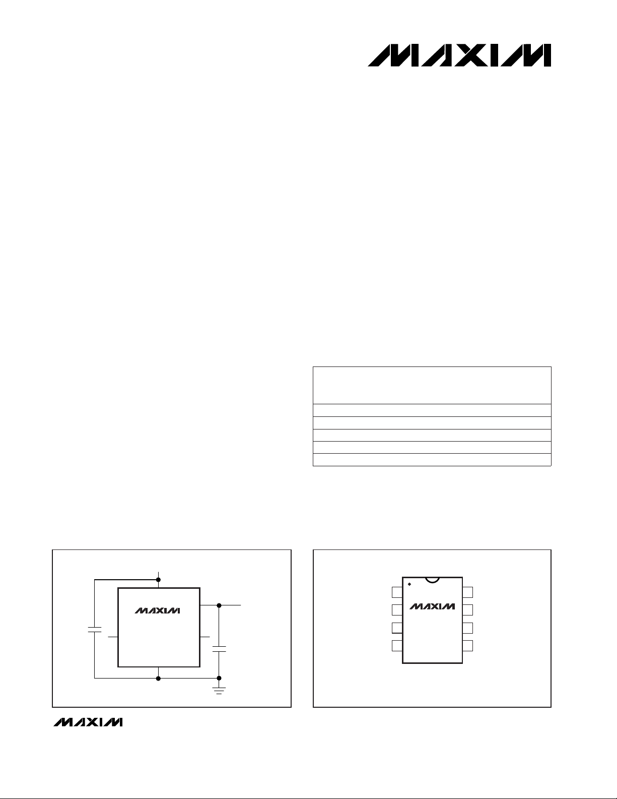
REFERENCE OUT
GND
NR
*OPTIONAL
TRIM
OUT
IN
8V TO 36V INPUT
*
2.2µF
*
2.2µF
MAX6325
MAX6341
MAX6350
__________Typical Operating Circuit
OUT
NR
TRIM
GND
1
2
8
7
I.C.
I.C.
IN
I.C.
MAX6325
MAX6341
MAX6350
DIP/SO
TOP VIEW
I.C. = INTERNALLY CONNECTED; DO NOT USE
3
4
6
5
__________________Pin Configuration
19-1203; Rev 0; 4/97
______________Ordering Information
Ordering Information continued at end of data sheet.
For free samples & the latest literature: http://www.maxim-ic.com, or phone 1-800-998-8800
MAX6325CPA
MAX6325CSA 0°C to +70°C
0°C to +70°C 1.0
1.0
8 Plastic DIP
8 SO
MAX6325EPA -40°C to +85°C 1.58 Plastic DIP
PART TEMP. RANGE
MAX
TEMPCO
(ppm/
°C)
PIN-
PACKAGE
MAX6325ESA -40°C to +85°C 1.58 SO
MAX6325MJA -55°C to +125°C 2.58 CERDIP

MAX6325/MAX6341/MAX6350
1ppm/°C, Low-Noise, +2.5V/+4.096V/+5V
Voltage References
2 _______________________________________________________________________________________
ABSOLUTE MAXIMUM RATINGS
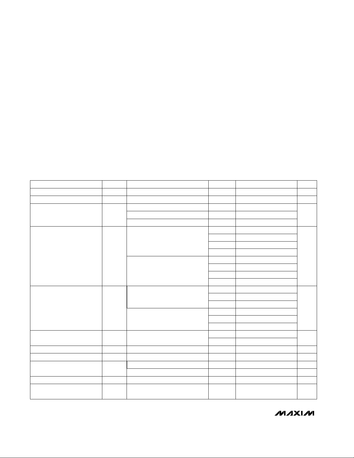
ELECTRICAL CHARACTERISTICS—MAX6325
(VIN= 10V, I
OUT
= 0mA, TA= T
MIN
to T
MAX
, unless otherwise noted. Typical values are at TA= +25°C.)
Stresses beyond those listed under “Absolute Maximum Ratings” may cause permanent damage to the device. These are stress ratings only, and functional
operation of the device at these or any other conditions beyond those indicated in the operational sections of the specifications is not implied. Exposure to
absolute maximum rating conditions for extended periods may affect device reliability.
(Voltages Referenced to GND)
IN................................................................................-0.3V to 40V
OUT, TRIM..................................................................-0.3V to 12V
NR.................................................................................-0.3V to 6V
OUT Short Circuit to GND Duration (V
IN
≤ 12V)..........Continuous
OUT Short Circuit to GND Duration (V
IN
≤ 40V) ....................5sec
OUT Short Circuit to IN Duration (V
IN
≤ 12V) ..............Continuous
Continuous Power Dissipation (T
A
= +70°C)
Plastic DIP (derate 9.09mW/°C above +70°C)................727mW
SO (derate 5.88mW/°C above +70°C)............................471mW
CERDIP (derate 8.00mW/°C above +70°C)....................640mW
Operating Temperature Ranges
MAX63_ _ C_ A.......................................................0°C to +70°C
MAX63_ _ E_ A....................................................-40°C to +85°C
MAX63_ _ MJA..................................................-55°C to +125°C
Storage Temperature Range ..............................-65°C to +150°C
Lead Temperature (soldering, 10sec)...............................+300°C
Load Regulation (Note 2)
∆V
OUT
/
∆I
OUT
ppm/mA
+25°C
+25°C
µs5+25°Ct
ON
Turn-On Settling Time To ±0.01% of final value
µV
RMS
1.3 2.8+25°C
e
n
Output Noise Voltage (Note 3)
µVp-p1.5
mV±15 ±25C, E, M∆V
OUT
Trim-Adjustment Range
mA
3.0C, E, M
I
IN
Supply Current
1.8 2.7+25°C
10 30M
1 7
10Hz ≤ f ≤ 1kHz
E
0.1Hz ≤ f ≤ 10Hz
Figure 1
1 6C
ppm/
1000h
3 15M
30+25°C
1 7
∆V
OUT
/ tLong-Term Stability
E
1 6C
+25°CTemperature Hysteresis ppm20(Note 4)
10M
8E
7C
2 5+25°C
10V ≤ VIN≤ 36V
45M
35E
30C
MAX6325MJA 1.0 2.5M
8V ≤ VIN≤ 10V
CONDITIONS
MAX6325E_A
MAX6325C_A
MAX6325
ppm/V
10 18+25°C
∆V
OUT
/
∆
V
IN
Line Regulation (Note 2)
ppm/°C0.75 1.5ETCV
OUT
Output Voltage Temperature
Coefficient (Note 1)
0.5 1.0C
Output Voltage V
OUT
2.499 2.500 2.501 V
T
A
C, E, M
PARAMETER SYMBOL MIN TYP MAX UNITS
Input Voltage Range V
IN
8 36 V
Sourcing: 0mA ≤ I
OUT
≤ 15mA
Sinking: -15mA ≤ I
OUT
≤ 0mA

MAX6325/MAX6341/MAX6350
1ppm/°C, Low-Noise, +2.5V/+4.096V/+5V
Voltage References
_______________________________________________________________________________________ 3
(Note 4)
V4.095 4.096 4.097V
OUT
Output Voltage +25°C
20 ppmTemperature Hysteresis
C 0.5 1.0
MAX6341
Output Voltage Temperature
Coefficient (Note 1)
TCV
OUT
E 0.75 1.5
ppm/°C
+25°C
+25°C 10 18
MAX6341C_A
MAX6341E_A
CONDITIONS
30
ppm/
1000h
8V ≤ VIN≤ 10V
Long-Term Stability ∆V
OUT
/ t +25°C
Line Regulation (Note 2)
∆V
OUT
/
∆V
IN
ppm/V
Figure 1
0.1Hz ≤ f ≤ 10Hz
10Hz ≤ f ≤ 1kHz
V8 36V
IN
Input Voltage Range
+25°C 1.9 2.9
I
IN
C, E, M 3.2
mA
Trim-Adjustment Range
UNITSMIN TYP MAXSYMBOLPARAMETER
∆V
OUT
C, E, M ±24 ±40 mV
2.4 µVp-p
Output Noise Voltage (Note 3) e
n
+25°C
2.0 4.0 µV
RMS
C, E, M
T
A
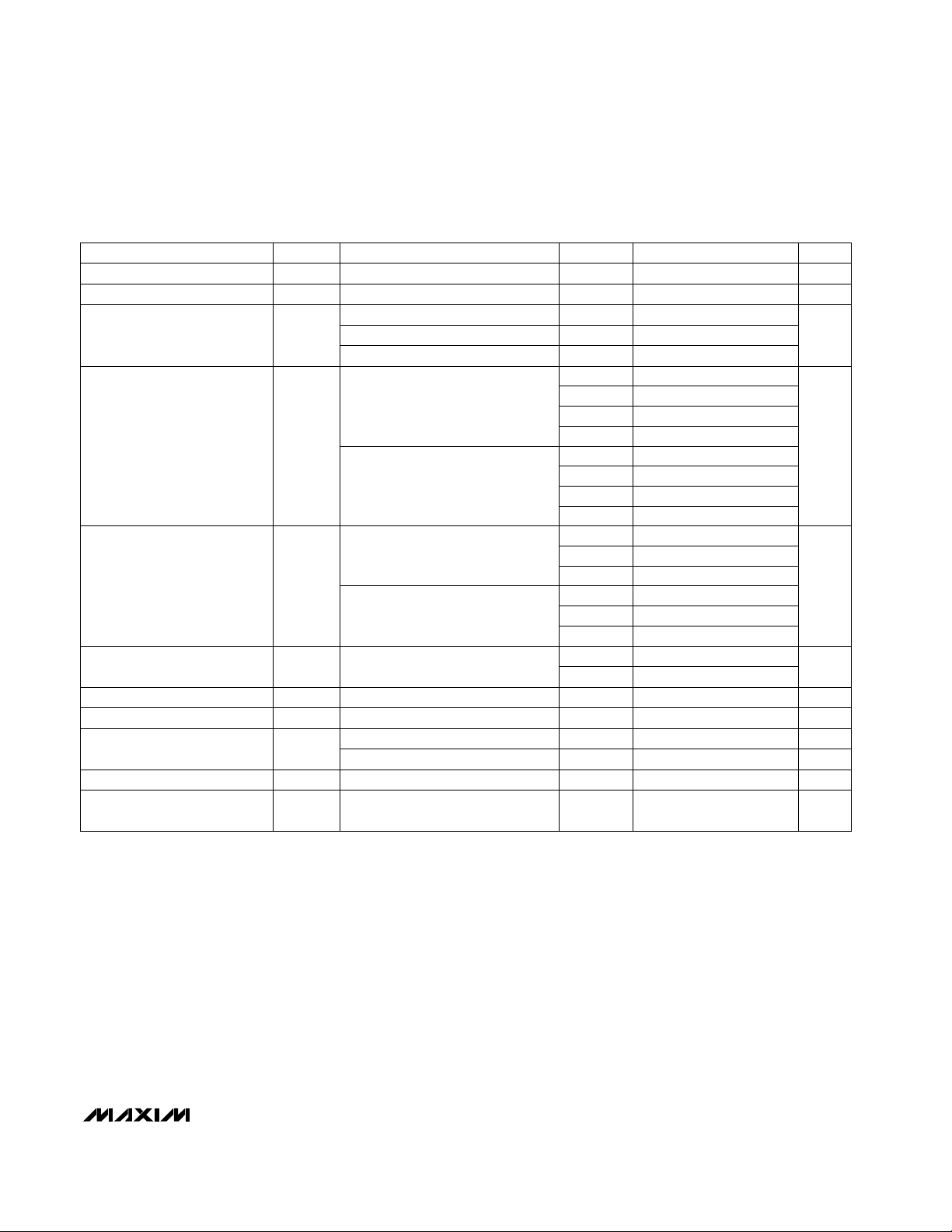
ELECTRICAL CHARACTERISTICS—MAX6341
(VIN= 10V, I
OUT
= 0mA, TA= T
MIN
to T
MAX
, unless otherwise noted. Typical values are at TA= +25°C.)
M 1.0 2.5MAX6341MJA
To ±0.01% of final valueTurn-On Settling Time t
ON
+25°C 8 µs
C 30
E 35
M 45
+25°C 2 5
10V ≤ VIN≤ 36V
C 7
E 8
M 10
Supply Current
C 1 6
E 1 7
M 3 9
C 1 6
E 1 7
M 7 18
+25°C
Sourcing: 0mA ≤ I
OUT
≤ 15mA
Sinking: -15mA ≤ I
OUT
≤ 0mA
∆V
OUT
/
∆I
OUT
Load Regulation (Note 2) ppm/mA

MAX6325/MAX6341/MAX6350
1ppm/°C, Low-Noise, +2.5V/+4.096V/+5V
Voltage References
4 _______________________________________________________________________________________
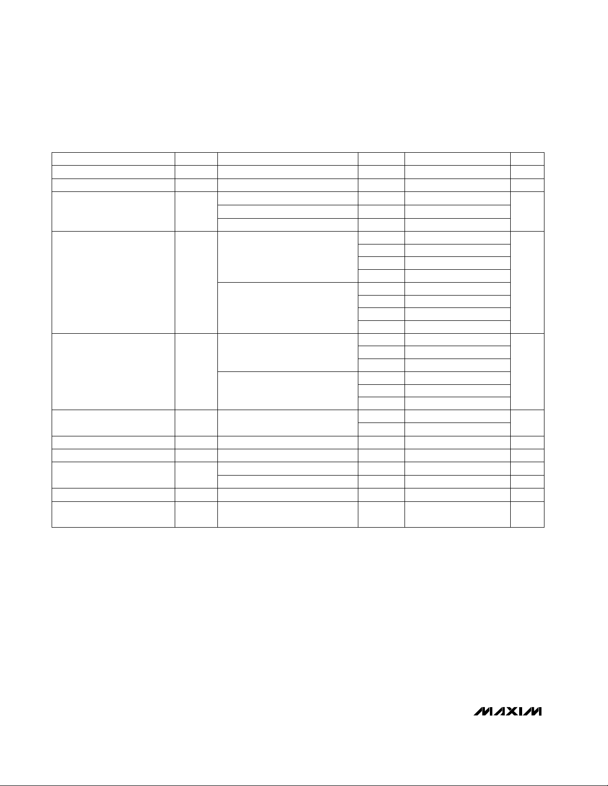
ELECTRICAL CHARACTERISTICS—MAX6350
(VIN= 10V, I
OUT
= 0mA, TA= T
MIN
to T
MAX
, unless otherwise noted. Typical values are at TA= +25°C.)
(Note 4)
V4.999 5.000 5.001V
OUT
Output Voltage +25°C
20 ppmTemperature Hysteresis
C 0.5 1.0
MAX6350
E 0.75 1.5
+25°C
+25°C 10 18
MAX6350C_A
MAX6350E_A
CONDITIONS
30
ppm/
1000h
8V ≤ VIN≤ 10V
Long-Term Stability ∆V
OUT
/ t +25°C
Line Regulation (Note 2)
∆V
OUT
/
∆V
IN
ppm/V
Figure 1
To ±0.01% of final value
V8 36V
IN
Input Voltage Range
+25°C 2.0 3.0
Supply Current I
IN
C, E, M 3.3
mA
Trim-Adjustment Range
UNITSMIN TYP MAXSYMBOLPARAMETER
∆V
OUT
C, E, M ±30 ±50 mV
10 µsTurn-On Settling Time t
on
+25°C
C, E, M
T
A
C 30
E 35
M 45
C 7
+25°C 2 5
E 8
10V ≤ VIN≤ 36V
M 10
C 1 6
C 1 6
E 1 7
E 1 7
M
M 2 9
6 15
0.1Hz ≤ f ≤ 10Hz
10Hz ≤ f ≤ 1kHz
3.0 µVp-p
Output Noise Voltage (Note 3) e
n
+25°C
2.5 5.0 µV
RMS
Output Voltage Temperature
Coefficient (Note 1)
TCV
OUT
ppm/°C
M 1.0 2.5MAX6350MJA
Note 1: Temperature coefficient is measured by the box method; i.e., the maximum ∆V
OUT
is divided by ∆T x V
OUT
.
Note 2: Line regulation (∆V
OUT
/ (V
OUT
x ∆
VIN
)) and load regulation (∆V
OUT
/ (V
OUT
x ∆I
OUT
)) are measured with pulses and do not
include output voltage changes due to die-temperature changes.
Note 3: Noise specifications are 100% tested for the 10Hz to 1kHz bandwidth. Production testing in the 0.1Hz to 10Hz bandwidth is
available upon request.
Note 4: Temperature hysteresis is specified at T
A
= +25°C by measuring V
OUT
before and after changing temperature by +25°C
using the plastic DIP package.
+25°C
Sourcing: 0mA ≤ I
OUT
≤ 15mA
Sinking: -15mA ≤ I
OUT
≤ 0mA
ppm/mA
∆V
OUT
/
∆I
OUT
Load Regulation (Note 2)
 Loading...