RESET
RESET
19-1078; Rev 0; 6/96
+5V, Low-Power µP Supervisory Circuits
with Adjustable Reset/Watchdog
_______________General Description
The MAX6301/MAX6302/MAX6303/MAX6304* lowpower microprocessor (µP) supervisory circuits provide
maximum adjustability for reset and watchdog functions.
The reset threshold can be adjusted to any voltage
above 1.22V, using external resistors. In addition, the
reset and watchdog timeout periods are adjustable
using external capacitors. A watchdog select pin
extends the watchdog timeout period to 500x. The reset
function features immunity to power-supply transients.
These four devices differ only in the structure of their reset
outputs (see
Selector Guide
). The MAX6301–MAX6304
are available in the space-saving 8-pin µMAX package,
as well as 8-pin DIP/SO.
________________________Applications
Medical Equipment Embedded Controllers
Intelligent Instruments Critical µP Monitoring
Portable Equipment Set-Top Boxes
Battery-Powered Computers
Computers/Controllers
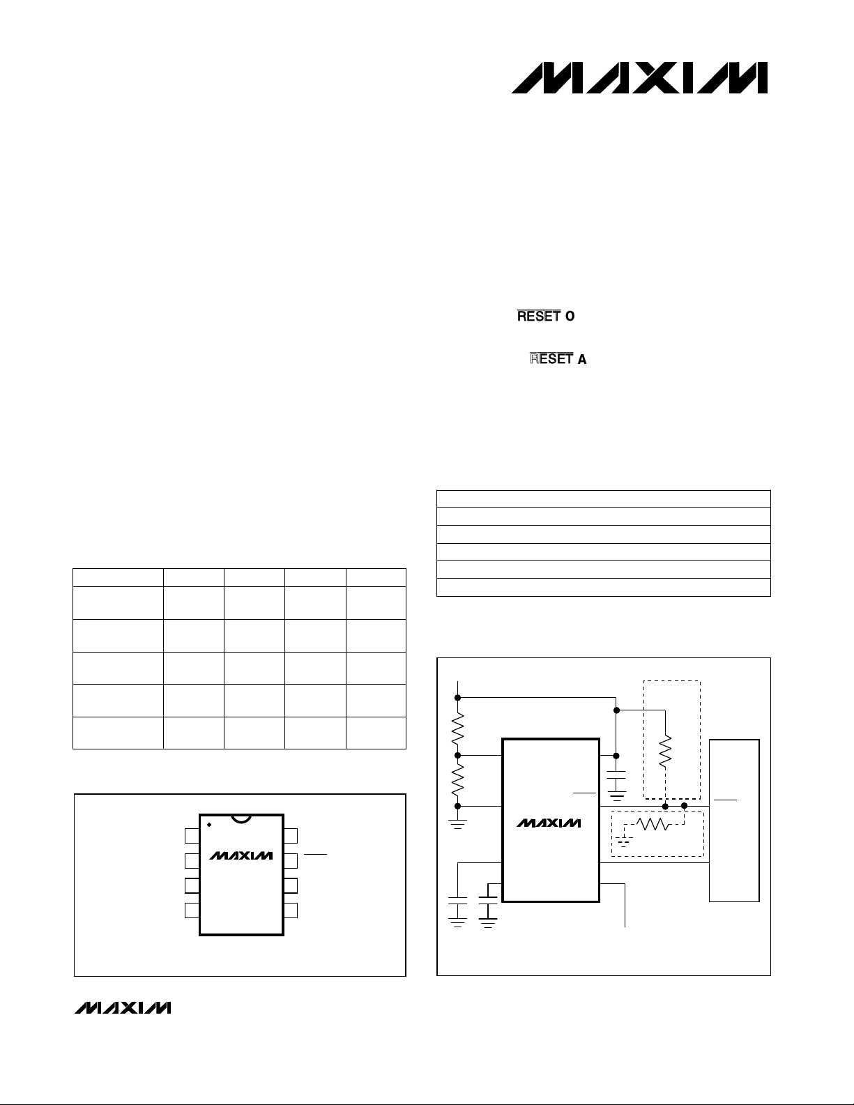
_____________________Selector Guide
FEATURE MAX6301 MAX6302 MAX6303 MAX6304
Active-Low
Reset
Active-High
Reset
Open-Drain
Reset Output
Push/Pull
Reset Output
Pins-Package
✓
—
✓ ✓
— —
8-DIP/SO/
µMAX
—
✓
8-DIP/SO/
µMAX
✓
—
— —
✓ ✓
8-DIP/SO/
µMAX
—
✓
8-DIP/SO/
µMAX
__________________Pin Configuration
TOP VIEW
RESET IN
( ) ARE FOR MAX6302/MAX6304.
* Patents pending
1
GND
2
MAX6301
SRT
SWT
MAX6302
3
MAX6303
MAX6304
4
DIP/SO/µMAX
________________________________________________________________
V
8
CC
RESET (RESET)
7
WDI
6
WDS
5
____________________________Features
♦ Adjustable Reset Threshold
♦ Adjustable Reset Timeout
♦ Adjustable Watchdog Timeout
♦ 500x Watchdog Timeout Multiplier
♦ 4µA Supply Current
♦ RESET or
♦ Push/Pull or Open-Drain Output Options
♦ Guaranteed
= 1V (MAX6301/MAX6303)
V
CC
Output Options
Asserted At or Above
♦ Power-Supply Transient Immunity
♦ Watchdog Function Can Be Disabled
♦ DIP/SO/µMAX Packages Available
______________Ordering Information
PART
MAX6301CPA
MAX6301CSA
MAX6301CUA 0°C to +70°C
MAX6301EPA
MAX6301ESA -40°C to +85°C
Ordering Information continued at end of data sheet.
TEMP. RANGE PIN-PACKAGE
0°C to +70°C
0°C to +70°C
-40°C to +85°C 8 Plastic DIP
8 Plastic DIP
8 SO
8 µMAX
8 SO
__________Typical Operating Circuit
V
IN
MAX6301
ONLY
R1
1
RESET IN
R2
2
GND
3
SRT
4
SWT
C
C
SWT
SRT
( ) ARE FOR MAX6302/MAX6304.
MAX6301
MAX6302
MAX6303
MAX6304
8
V
CC
0.1µF
RESET
7
(RESET)
6
WDI
5
WDS
Maxim Integrated Products
R
R
MAX6302
L
ONLY
WDS = 0 FOR NORMAL MODE
WDI = 1 FOR EXTENDED MODE
L
RESET
µP
I/O
MAX6301–MAX6304
1
For free samples & the latest literature: http://www.maxim-ic.com, or phone 1-800-998-8800

+5V, Low-Power µP Supervisory Circuits
with Adjustable Reset/Watchdog
ABSOLUTE MAXIMUM RATINGS
VCC.......................................................................-0.3V to +7.0V
RESET IN, SWT, SRT..................................-0.3V to (V
WDI, WDS..............................................................-0.3V to +7.0V
RESET, RESET
MAX6301...........................................................-0.3V to +7.0V
MAX6302/6303/6304..............................-0.3V to (V
Input Current
...............................................................................±20mA
V
CC
GND..............................................................................±20mA
Output Current
RESET, RESET..............................................................±20mA
Stresses beyond those listed under “Absolute Maximum Ratings” may cause permanent damage to the device. These are stress ratings only, and functional
operation of the device at these or any other conditions beyond those indicated in the operational sections of the specifications is not implied. Exposure to
absolute maximum rating conditions for extended periods may affect device reliability.
CC
CC
+ 0.3V)
+ 0.3V)
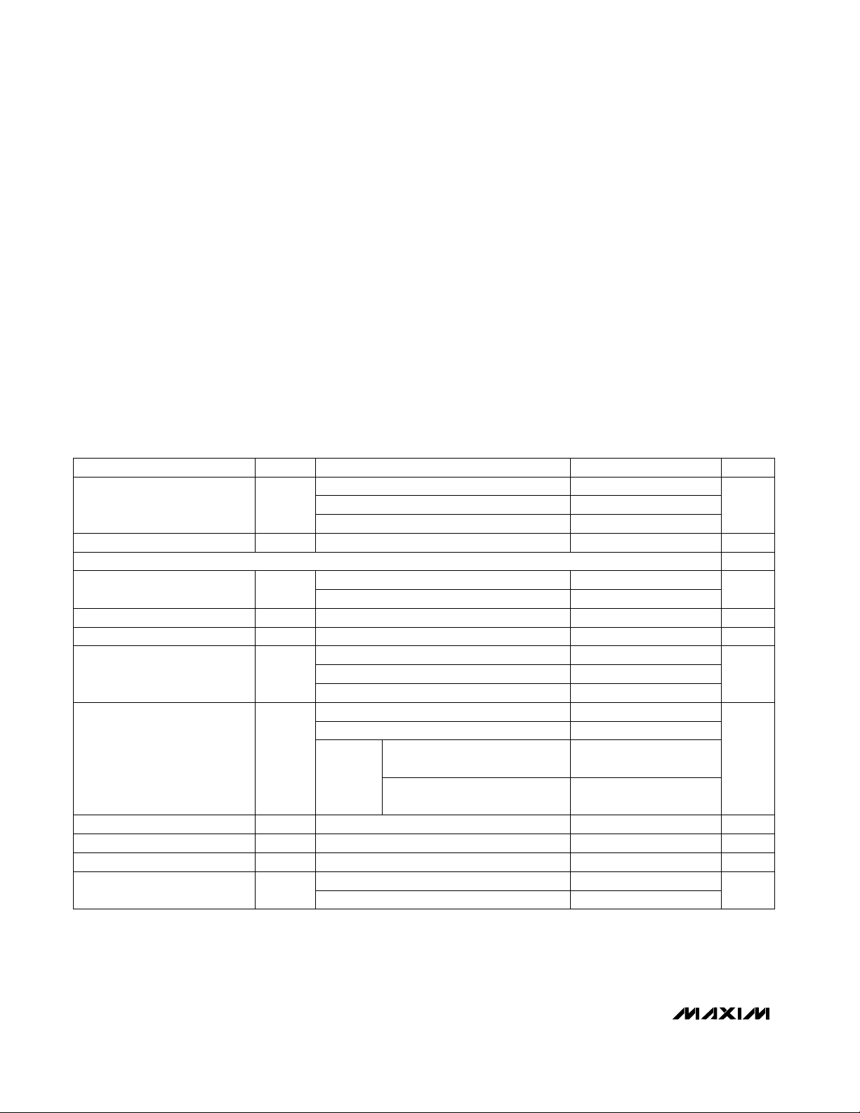
ELECTRICAL CHARACTERISTICS
(VCC= +2V to +5.5V, TA= T
MIN
to T
, unless otherwise noted. Typical values are at VCC= +5V and TA= +25°C.)
MAX
MAX6301–MAX6304
Operating Voltage Range
(Note 1)
Supply Current (Note 2)
RESET TIMER
Reset Input Threshold Voltage
Reset Input Hysteresis
Reset Input Leakage Current
Reset Output Voltage High
(MAX6302/MAX6303/MAX6304)
Reset Output Voltage Low
(MAX6301/MAX6303/MAX6304)
VCCto Reset Delay
Reset Input Pulse Width
Reset Timeout Period (Note 3)
Reset Output Leakage Current
V
V
HYST
RESET IN
V
V
MAX6301C/MAX6303C
MAX6301E/MAX6303E
CC
MAX6302/MAX6304
No load
CC
V
TH
OH
OL
RD
RI
RP
RESET IN
V
RESET IN
VCC≥ 4.5V, I
VCC= 2V, I
MAX6302/MAX6304, VCC= 1.31V, RL= 10kΩ
VCC≥ 4.5V, I
VCC= 2V, I
MAX6301/
MAX6303
VCCfalling at 1mV/µs
Comparator overdrive = 50mV
C
SRT
MAX6301, V
MAX6302, V
falling, VCC= 5.0V
rising, VCC= 5.0V
SOURCE
SOURCE
SINK
SINK
VCC= 1V, I
TA= 0°C to +70°C
VCC= 1.2V, I
TA= -40°C to +85°C
= 1500pF
RESET
RESET
Continuous Power Dissipation (TA= +70°C)
Plastic DIP (derate 9.09mW/°C above +70°C) ............727mW
SO (derate 5.88mW/°C above +70°C).........................471mW
µMAX (derate 4.10mW/°C above +70°C) ....................330mW
Operating Temperature Ranges
MAX630_C_A......................................................0°C to +70°C
MAX630_E_A...................................................-40°C to +85°C
Storage Temperature Range.............................-65°C to +160°C
Lead Temperature (soldering, 10sec).............................+300°C
CONDITIONS
1.00 5.50
1.20 5.50
1.31 5.50
1.195 1.220 1.245
1.240 1.265
= 0.8mA
= 0.4mA
= 3.2mA
= 1.6mA
= V
CC
= GND
SINK
SINK
= 50µA,
= 100µA,
VCC- 0.4
VCC - 0.4
VCC- 0.3
0.4
0.4
0.3
0.3
±1
±1
UNITSMIN TYP MAXSYMBOLPARAMETER
V
µA4.0 7.0I
V
mV20V
nA±0.01 ±1I
V
V
µs63t
µs26t
ms2.8 4.0 5.2t
µA
2 _______________________________________________________________________________________

+5V, Low-Power µP Supervisory Circuits
with Adjustable Reset/Watchdog
ELECTRICAL CHARACTERISTICS (continued)
(VCC= +2V to +5.5V, TA= T
WATCHDOG TIMER
WDI, WDS Input Threshold
WDI Pulse Width
WDI, WDS Leakage Current Extended mode disabled ±1 µA
WDI Sink/Source Current
(Note 4)
Watchdog Timeout Period
(Note 3)
Note 1: Reset is guaranteed valid from the selected reset threshold voltage down to the minimum VCC.
Note 2: VDS = V
, WDI unconnected.
CC
Note 3: Precision timing currents of 500nA are present at both the SRT and SWT pins. Timing capacitors connected to these nodes
must have low leakage consistent with these currents to prevent timing errors.
Note 4: The sink/source is supplied through a resistor, and is proportional to V
MIN
to T
, unless otherwise noted. Typical values are at VCC= +5V and TA= +25°C.)
MAX
CONDITIONS
V
t
V
IH
IL
VCC= 4.5V to 5.5V
WP
VCC= 2V to 4.5V 60
0.7V
Extended mode enabled ±70 µA
t
WD
WDS = GND, C
WDS = VCC, C
= 1500pF 2.8 4.0 5.2
SWT
= 1500pF 1.4 2.0 2.6 sec
SWT
(Figure 8). At VCC= 2V, it is typically ±24µA.
CC
30
CC
0.3V
CC
UNITSMIN TYP MAXSYMBOLPARAMETER
V
ns
ms
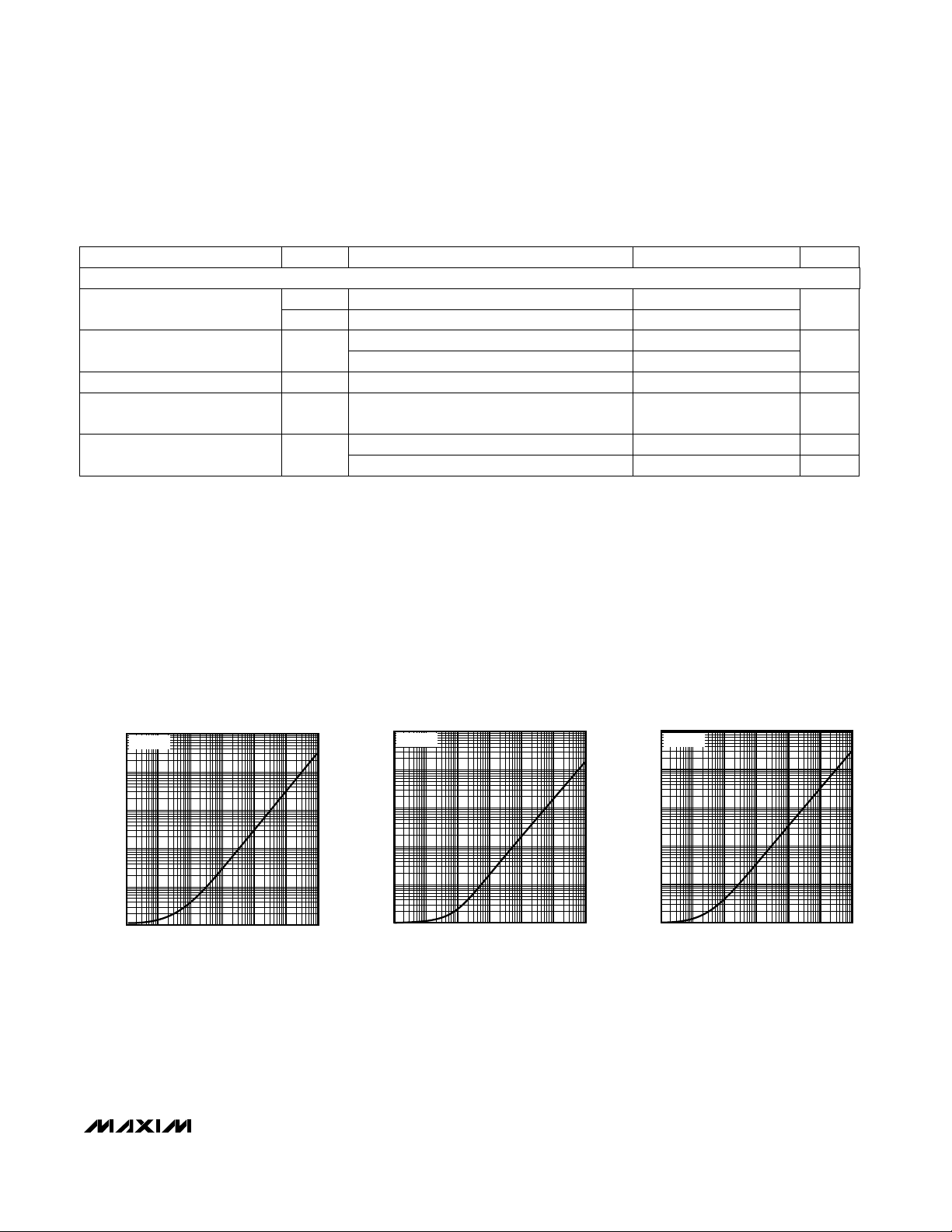
__________________________________________Typical Operating Characteristics
(C
SWT
= C
= 1500pF, TA= +25°C, unless otherwise noted.)
SRT
MAX6301–MAX6304
RESET TIMEOUT PERIOD
vs. C
10,000
VCC = 5V
1000
100
10
1
RESET TIMEOUT PERIOD (ms)
0
0.001 0.01 0.1 1 10 100 1000
SRT
C
(nF)
SRT
_______________________________________________________________________________________
WATCHDOG TIMEOUT PERIOD vs. C
10,000
6301-4 TOC-01
VCC = 5V
1000
100
10
1
WATCHDOG TIMEOUT PERIOD (sec)
0
0.001 0.01 0.1 1 10 100 1000
EXTENDED-MODE
(WDS = V
C
SWT
(nF)
)
CC
SWT
6301-4 TOC-02
WATCHDOG TIMEOUT PERIOD vs. C
10,000
VCC = 5V
1000
100
10
1
WATCHDOG TIMEOUT PERIOD (ms)
0.1
0.001 0.01 0.1 1 10 100 1000
NORMAL-MODE
(WDS = GND)
C
(nF)
SWT
SWT
6301-4 TOC-03
3

+5V, Low-Power µP Supervisory Circuits
with Adjustable Reset/Watchdog
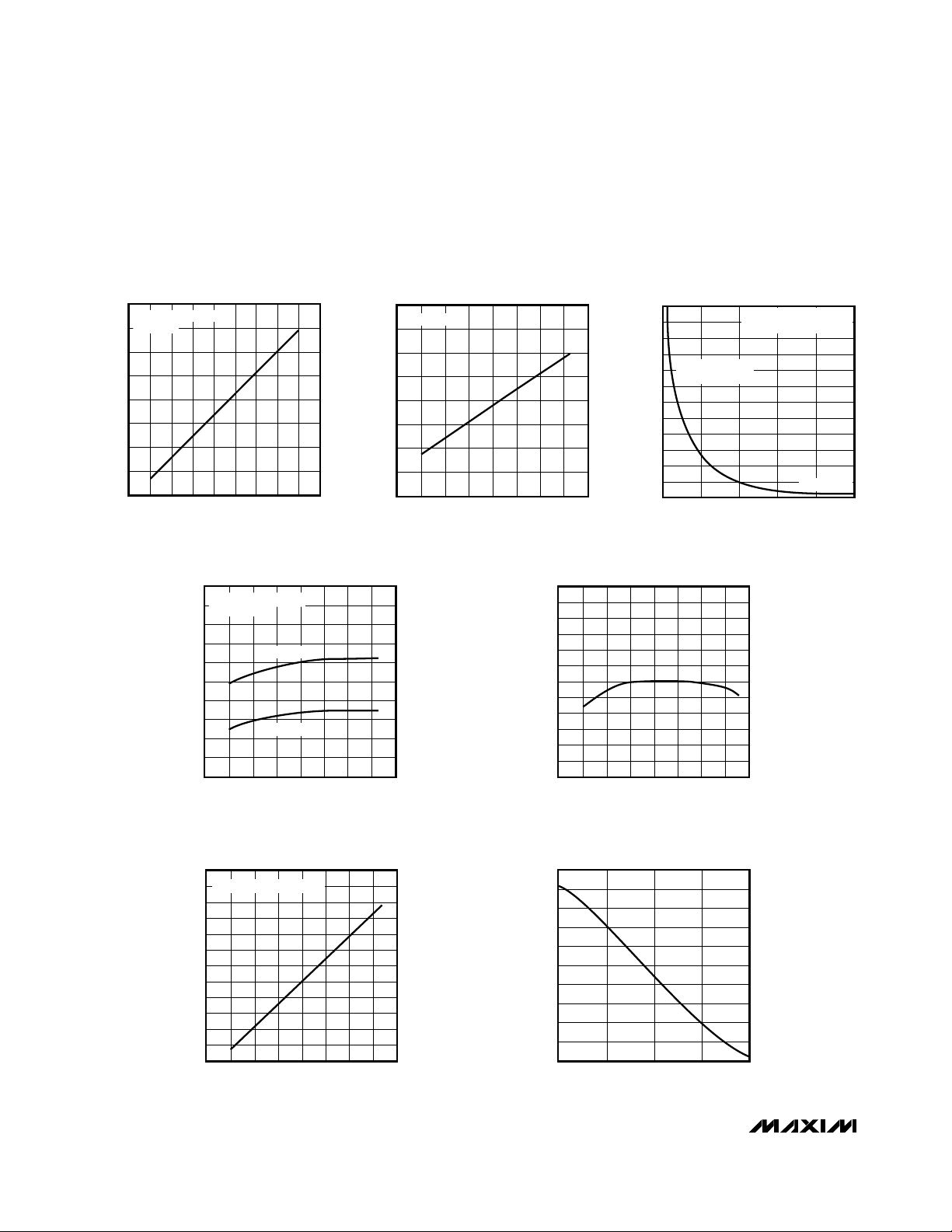
____________________________Typical Operating Characteristics (continued)
(C
= C
SWT
4.2
4.0
3.8
3.6
3.4
3.2
SUPPLY CURRENT (µA)
3.0
2.8
2.6
MAX6301–MAX6304
= 1500pF, TA= +25°C, unless otherwise noted.)
SRT
SUPPLY CURRENT vs.
SUPPLY VOLTAGE
RESET DEASSERTED
NO LOAD
3.0 5.01.5 2.5 4.53.5 5.5
SUPPLY VOLTAGE (V)
6.02.0 4.0
6301-4 TOC-04
(ms)
WD
/t
RP
t
WATCHDOG TIMEOUT PERIOD
4.20
VCC = 5.0V
4.15
4.10
4.05
4.00
3.95
3.90
3.85
3.80
-40 40
RESET AND NORMAL-MODE
vs. TEMPERATURE
080-60 -20 6020 100
TEMPERATURE (°C)
6301-4 TOC-05
MAXIMUM TRANSIENT DURATION vs.
RESET THRESHOLD OVERDRIVE (V
120
110
100
90
RESET OCCURS
80
ABOVE THE CURVE
70
60
50
40
30
TRANSIENT DURATION (µs)
20
10
0
0 200 400 600 1000800
RESET THRESHOLD OVERDRIVE (mV)
SEE
NEGATIVE-GOING VCC
TRANSIENTS
SECTION
V
RST
RST
= 4.60V
)
6301-4 TOC-06
5.00
4.75
4.50
4.25
4.00
3.75
3.50
3.25
SUPPLY CURRENT (µA)
3.00
2.75
2.50
76
72
68
64
60
PROPAGATION DELAY (µs)
56
SUPPLY CURRENT
vs. TEMPERATURE
RESET DEASSERTED
NO LOAD
VCC = 5.0V
VCC = 2.0V
-40 40
080-60 -20 6020 100
TEMPERATURE (°C)
VCC TO RESET DELAY
vs. TEMPERATURE (V
VCC FALLING AT 1mV/µs
FALLING)
CC
6301-4 TOC-07
6301-4 TOC-09
RESET IN THRESHOLD VOLTAGE
vs. TEMPERATURE
1.226
1.224
1.222
1.220
1.218
1.216
RESET REFERENCE VOLTAGE (V)
1.214
-40 40
080-60 -20 6020 100
TEMPERATURE (°C)
RESET AND WATCHDOG
TIMEOUT vs. V
4.16
4.12
4.08
(ms)
WP
/t
RP
4.04
t
4.00
6301-4 TOC-08
CC
6301-4 TOC-10
52
-40 40
080-60 -20 6020 100
TEMPERATURE (°C)
3.96
23 546
SUPPLY VOLTAGE (V)
4 _______________________________________________________________________________________
 Loading...