

Page 1
General Description
Maxim’s MAX630 and MAX4193 CMOS DC-DC regulators are designed for simple, efficient, minimum-size
DC-DC converter circuits in the 5mW to 5W range. The
MAX630 and MAX4193 provide all control and power
handling functions in a compact 8-pin package: a
1.31V bandgap reference, an oscillator, a voltage comparator, and a 375mA N-channel output MOSFET. A
comparator is also provided for low-battery detection.
Operating current is only 70µA and is nearly independent of output switch current or duty cycle. A logic-level
input shuts down the regulator to less than 1µA quiescent current. Low-current operation ensures high efficiency even in low-power battery-operated systems.
The MAX630 and MAX4193 are compatible with most
battery voltages, operating from 2.0V to 16.5V.
The devices are pin compatible with the Raytheon bipolar circuits, RC4191/2/3, while providing significantly
improved efficiency and low-voltage operation. Maxim
also manufactures the MAX631, MAX632, and MAX633
DC-DC converters, which reduce the external component count in fixed-output 5V, 12V, and 15V circuits.
See Table 2 at the end of this data sheet for a summary
of other Maxim DC-DC converters.
Applications
+5V to +15V DC-DC Converters
High-Efficiency Battery-Powered DC-DC
Converters
+3V to +5V DC-DC Converters
9V Battery Life Extension
Uninterruptible 5V Power Supplies
5mW to 5W Switch-Mode Power Supplies
Features
♦ High Efficiency—85% (typ)
♦ 70µA Typical Operating Current
♦ 1µA Maximum Quiescent Current
♦ 2.0V to 16.5V Operation
♦ 525mA (Peak) Onboard Drive Capability
♦ ±1.5% Output Voltage Accuracy (MAX630)
♦ Low-Battery Detector
♦ Compact 8-Pin Mini-DIP and SO Packages
♦ Pin Compatible with RC4191/2/3
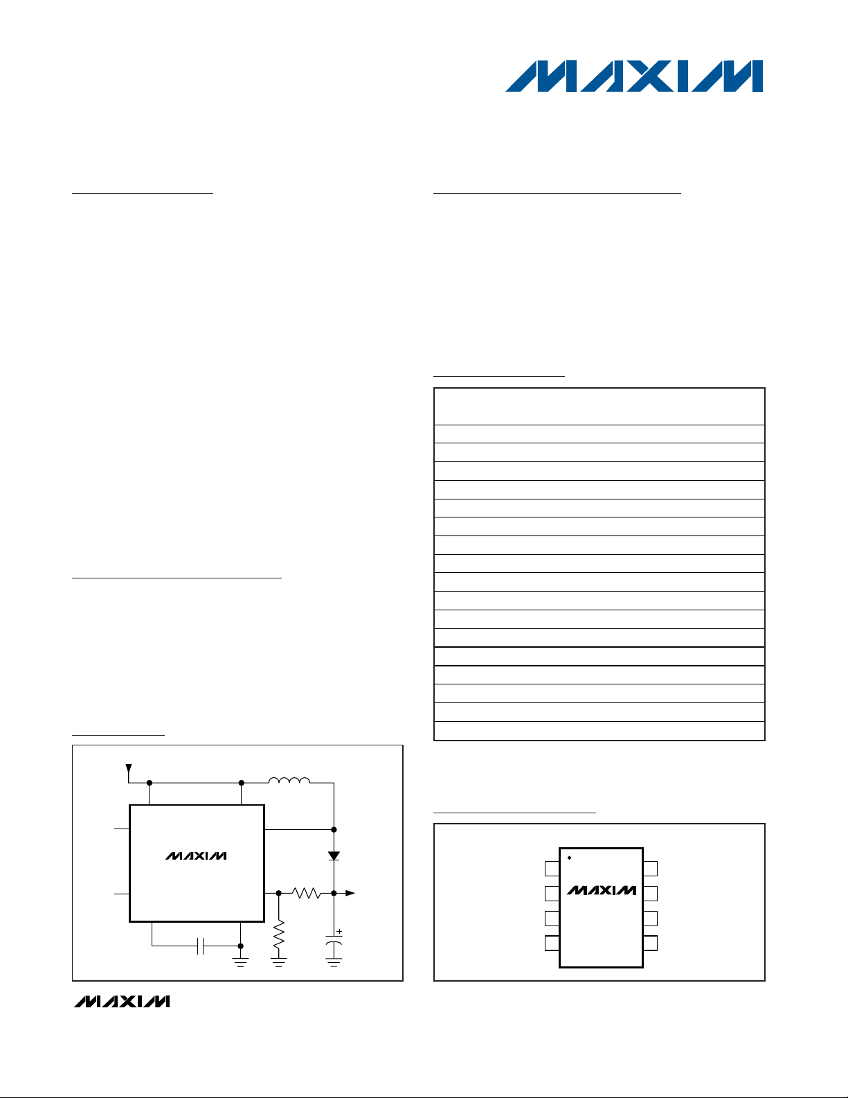
MAX630/MAX4193
CMOS Micropower Step-Up
Switching Regulator
________________________________________________________________ Maxim Integrated Products 1
I
C
+V
S
GND
1
2
87LBD
V
FB
C
X
L
X
LBR
TOP VIEW
3
4
6
5
MAX630
MAX4193
Pin Configuration
Ordering Information
MAX630
+5V IN
470μH
+15V
OUT
47pF
8
LBD
1
LBR
2
C
X
4
GND
7
V
FB
3
L
X
6
I
C
5
+V
S
+5 TO +15V CONVERTER
Typical Operating Circuit
19-0915; Rev 2; 9/08
For pricing, delivery, and ordering information, please contact Maxim/Dallas Direct! at
1-888-629-4642, or visit Maxim’s website at www.maxim-ic.com.
*Dice are specified at TA= +25°C. Contact factory for dice
specifications.
**Contact factory for availability and processing to MIL-STD-883.
†Contact factory for availibility.
PART TEMP RANGE
MAX630CPA 0°C to +70°C 8 PDIP
MAX630CSA 0°C to +70°C 8 SO
MAX630CJA 0°C to +70°C 8 CERDIP
MAX630EPA -40°C to +85°C 8 PDIP
MAX630ESA -40°C to +85°C 8 SO
MAX630EJA -40°C to +85°C 8 CERDIP
MAX630MJA -55°C to +125°C 8 CERDIP**
MAX630MSA/PR -55°C to +125°C 8 SO†
M AX 630M S A/P R- T -55°C to +125°C 8 SO†
MAX4193C/D 0°C to +70°C Dice*
MAX4193CPA 0°C to +70°C 8 PDIP
MAX4193CSA 0°C to +70°C 8 SO
MAX4193CJA 0°C to +70°C 8 CERDIP
MAX4193EPA -40°C to +85°C 8 PDIP
MAX4193ESA -40°C to +85°C 8 SO
MAX4193EJA -40°C to +85°C 8 CERDIP
MAX4193MJA -55°C to +125°C 8 CERDIP**
PINPACKAGE
Page 2
MAX630/MAX4193
CMOS Micropower Step-Up
Switching Regulator
2 _______________________________________________________________________________________
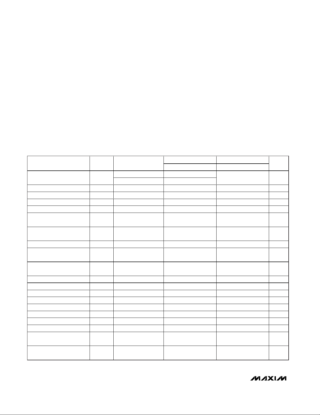
ABSOLUTE MAXIMUM RATINGS
ELECTRICAL CHARACTERISTICS
(+VS= +6.0V, TA= +25°C, IC= 5.0µA, unless otherwise noted.)
Stresses beyond those listed under “Absolute Maximum Ratings” may cause permanent damage to the device. These are stress ratings only, and functional
operation of the device at these or any other conditions beyond those indicated in the operational sections of the specifications is not implied. Exposure to
absolute maximum rating conditions for extended periods may affect device reliability.
Supply Voltage .......................................................................18V
Storage Temperature Range ............................-65°C to +160°C
Lead Temperature (soldering, 10s) .................................+300°C
Operating Temperature Range
MAX630C, MAX4193C........................................0°C to +70°C
MAX630E, MAX4193E .....................................-40°C to +85°C
MAX630M, MAX4193M..................................-55°C to +125°C
Power Dissipation
8-Pin PDIP (derate 6.25mW/°C above +50°C).............468mW
8-Pin SO (derate 5.88mW/°C above +50°C)................441mW
8-Pin CERDIP (derate 8.33mW/°C above +50°C)........833mW
Input Voltage (Pins 1, 2, 6, 7) .....................-0.3V to (+V
S
+ 0.3V)
Output Voltage, L
X
and LBD ..................................................18V
L
X
Output Current ..................................................525mA (Peak)
LBD Output Current ............................................................50mA
MAX630 MAX4193
PARAMETER
CONDITIONS
UNITS
Operating 2.0
Supply Voltage +V
S
Startup 1.9
2.4
V
Internal Reference Voltage V
REF
V
Switch Current I
SW
V3 = 400mV 75
75
mA
Supply Current (at Pin 5) I
S
I3 = 0mA 70
90 µA
Efficiency 85 85 %
Line Regulation
0.5V
0
< VS < V
0
(Note 1)
0.2
0.5
% V
OUT
Load Regulation
V
S
= +5V, P
LOAD
= 0 to
150mW (Note 1)
0.5 0.2 0.5
% V
OUT
Operating Frequency Range
F
O
(Note 2) 0.1 40 75 0.1 25 75 kHz
Reference Set Internal
Pulldown Resistance
R
IC
V6 = V
S
0.5
10 0.5 1.5 10 MΩ
Reference Set Input Voltage
Threshold
V
IC
0.2
1.3 0.2 0.8 1.3 V
Switch Current I
SW
V3 = 1.0V
mA
Switch Leakage Current I
CO
V3 = 16.5V
1.0
5.0 µA
Supply Current (Shutdown) I
SO
IC < 0.01µA
1.0
5.0 µA
Low-Battery Bias Current I
LBR
10
10 nA
Capacitor Charging Current I
CX
30 30 µA
CX+ Threshold Voltage +VS - 0.1 +VS - 0.1 V
CX- Threshold Voltage
0.1 V
VFB Input Bias Current I
FB
10
10 nA
Low-Battery Detector Output
Current
I
LBD
V8 = 0.4V, V1 = 1.1V
µA
Low-Battery Detector Output
Leakage
I
LBDO
V8 = 16.5V, V1 = 1.4V
5.0
5.0 µA
SYMBOL
MIN TYP MAX MIN TYP MAX
1.29 1.31 1.33 1.24 1.31 1.38
150
16.5
150
125
16.5
100 100
250 600 250 600
0.08
0.2
1.5
0.8
0.01
0.01
0.01
0.1
0.01
0.01
0.06
0.01
0.01
0.01
0.01
0.01
Page 3
MAX630/MAX4193
CMOS Micropower Step-Up
Switching Regulator
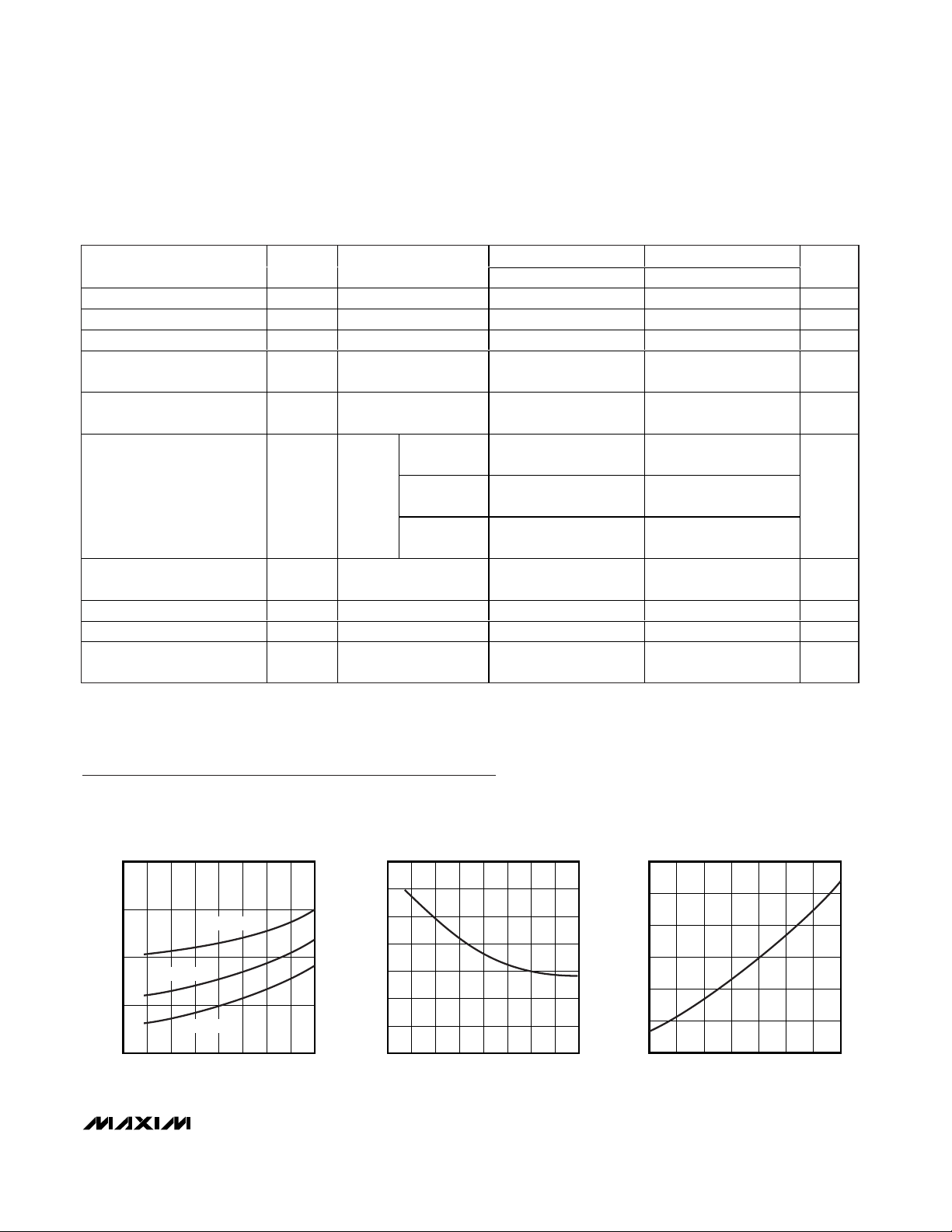
_______________________________________________________________________________________ 3
LX ON-RESISTANCE vs.
TEMPERATURE
MAX630/4193 toc01
TEMPERATURE (°C)
L
X
R
ON
(Ω)
1007550250-25-50
2
4
6
8
0
125
+VS = 2.5V
+VS = 6V
+VS = 16V
SUPPLY CURRENT vs.
TEMPERATURE
MAX630/4193 toc02
TEMPERATURE (°C)
I
S
(μA)
1007550250-25-50
40
20
80
60
120
100
140
0
125
SUPPLY CURRENT vs.
SUPPLY VOLTAGE
MAX630/4193 toc03
+VS (V)
I
S
(μA)
1412108642
50
150
100
250
200
300
16
Typical Operating Characteristics
(TA = +25°C, unless otherwise noted.)
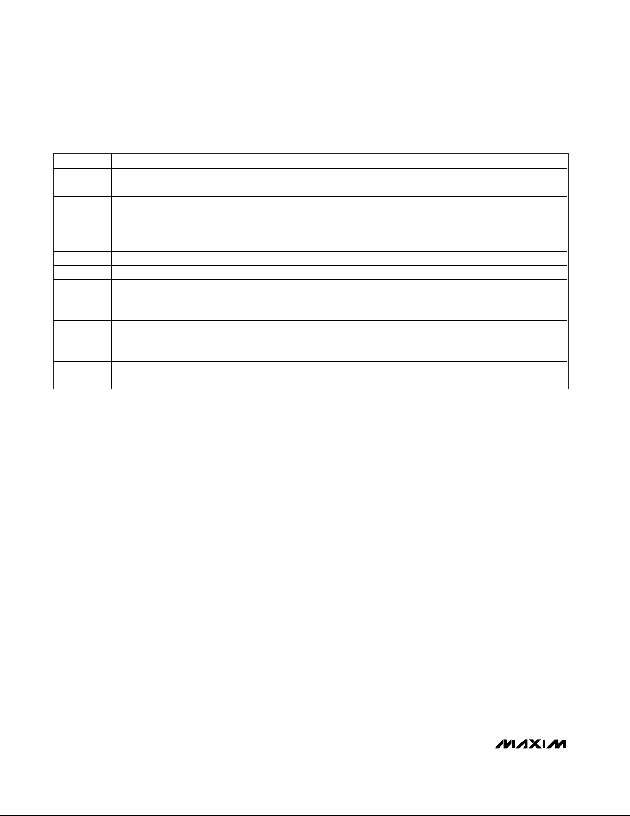
ELECTRICAL CHARACTERISTICS
(+VS= +6.0V, TA= Full Operating Temperature Range, IC= 5.0µA, unless otherwise noted.)
MAX630 MAX4193
PARAMETER
CONDITIONS
UNITS
Supply Voltage +V
S
V
Internal Reference Voltage V
REF
V
Supply Current (Pin 5) I
S
I3 = 0mA 70
90
µA
Line Regulation
0.5V
0UT
< VS < V
0UT
(Note 1)
0.5
1.0
% V
OUT
Load Regulation
V
S
= 0.5V0, PL = 0 to
150mW (Note 1)
1.0
1.0
% V
OUT
0°C ≤ TA ≤
+70°C
10
10
-40°C ≤ TA ≤
+85°C
10
10
Reference Set Internal
Pulldown Resistance
R
IC
-55°C ≤ TA ≤
+125°C
10
10
MΩ
Reference Set Input Voltage
Threshold
V
IC
1.3
1.3 V
Switch Leakage Current I
CO
V3 = 16.5V
30
30 µA
Supply Current (Shutdown) I
SO
IC < 0.01µA
10
30 µA
Low-Battery Detector Output
Current
I
LBD
V8 = 0.4V, V1 = 1.1V
µA
Note 1: Guaranteed by correlation with DC pulse measurements.
Note 2: The operating frequency range is guaranteed by design and verified with sample testing.
SYMBOL
V6 = V
S
MIN TYP MAX MIN TYP MAX
2.2 16.5 3.5 16.5
1.25 1.31 1.37 1.20 1.31 1.42
0.2
0.5
0.45 1.5
0.4 1.5
0.3 1.5
0.2 0.8
0.1
0.01
250 600 250 600
200
300
0.5
0.5
0.45 1.5
0.4 1.5
0.3 1.5
0.2 0.8
0.1
0.01
Page 4
Detailed Description
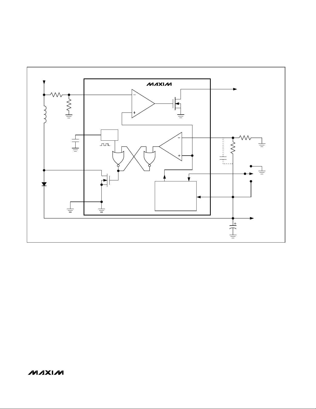
The operation of the MAX630 can best be understood
by examining the voltage regulating loop of Figure 1.
R1 and R2 divide the output voltage, which is compared with the 1.3V internal reference by comparator
COMP1. When the output voltage is lower than desired,
the comparator output goes high and the oscillator output pulses are passed through the NOR gate latch,
turning on the output N-channel MOSFET at pin 3, LX.
As long as the output voltage is less than the desired
voltage, pin 3 drives the inductor with a series of pulses
at the oscillator frequency.
Each time the output N-channel MOSFET is turned on,
the current through the external coil, L1, increases,
storing energy in the coil. Each time the output turns off,
the voltage across the coil reverses sign and the voltage at LXrises until the catch diode, D1, is forward
biased, delivering power to the output.
When the output voltage reaches the desired level,
1.31V x (1 + R1 / R2), the comparator output goes low
and the inductor is no longer pulsed. Current is then
supplied by the filter capacitor, C1, until the output voltage drops below the threshold, and once again LXis
switched on, repeating the cycle. The average duty
cycle at LXis directly proportional to the output current.
Output Driver (LX Pin)
The MAX630/MAX4193 output device is a large
N-channel MOSFET with an on-resistance of 4Ω and a
peak current rating of 525mA. One well-known advantage that MOSFETs have over bipolar transistors in
switching applications is higher speed, which reduces
switching losses and allows the use of smaller, lighter,
less costly magnetic components. Also important is that
MOSFETs, unlike bipolar transistors, do not require
base current that, in low-power DC-DC converters,
often accounts for a major portion of input power.
The operating current of the MAX630 and MAX4193
increases by approximately 1µA/kHz at maximum
power output due to the charging current required by
the gate capacitance of the LXoutput driver (e.g., 40µA
increase at a 40kHz operating frequency). In comparison, equivalent bipolar circuits typically drive their NPN
LXoutput device with 2mA of base drive, causing the
bipolar circuit’s operating current to increase by a factor of 10 between no load and full load.
Oscillator
The oscillator frequency is set by a single external, lowcost ceramic capacitor connected to pin 2, CX. 47pF
sets the oscillator to 40kHz, a reasonable compromise
between lower switching losses at low frequencies and
reduced inductor size at higher frequencies.
MAX630/MAX4193
CMOS Micropower Step-Up
Switching Regulator
4 _______________________________________________________________________________________
Pin Description
PIN NAME FUNCTION
1 LBR
Low-Battery Detection Comparator Input. The LBD output, pin 8, sinks current whenever this pin is
below the low-battery detector threshold, typically 1.31V.
2C
X
An external capacitor connected between this terminal and ground sets the oscillator frequency.
47pF = 40 kHz.
3L
X
This pin drives the external inductor. The internal N-channel MOSFET that drives LX has an output
resistance of 4Ω and a peak current rating of 525mA.
4 GND Ground
5+VSThe positive supply voltage, from 2.0V to 16.5V (MAX630).
6I
C
The MAX630/MAX4193 shut down when this pin is left floating or is driven below 0.2V. For normal
operation, connect I
C
directly to +VS or drive it high with either a CMOS gate or pullup resistor
connected to +V
S
. The supply current is typically 10nA in the shutdown mode
7V
FB
The output voltage is set by an external resistive divider connected from the converter output to V
FB
and ground. The MAX630/MAX4193 pulse the LX output whenever the voltage at this terminal is less
than 1.31V.
8 LBD
The Low-Battery Detector output is an open-drain N-channel MOSFET that sinks up to 600μA (typ)
whenever the LBR input, pin 1, is below 1.31V.
Page 5
Low-Battery Detector
The low-battery detector compares the voltage on LBR
with the internal 1.31V reference. The output, LBD, is an
open-drain N-channel MOSFET. In addition to detecting
and warning of a low battery voltage, the comparator
can also perform other voltage-monitoring operations
such as power-failure detection.
Another use of the low-battery detector is to lower the
oscillator frequency when the input voltage goes below
a specified level. Lowering the oscillator frequency
increases the available output power, compensating for
the decrease in available power caused by reduced
input voltage (see Figure 5).
Logic-Level Shutdown Input
The shutdown mode is entered whenever IC(pin 6) is
driven below 0.2V or left floating. When shut down, the
MAX630’s analog circuitry, oscillator, LX, and LBD outputs are turned off. The device’s quiescent current during shutdown is typically 10nA (1µA max).
Bootstrapped Operation
In most circuits, the preferred source of +VSvoltage for
the MAX630 and MAX4193 is the boosted output voltage. This is often referred to as a “bootstrapped” operation since the circuit figuratively “lifts” itself up.
The on-resistance of the N-channel LX output decreases with an increase in +VS; however, the device operating current goes up with +VS(see the Typical
Operating Characteristics, ISvs. +VSgraph). In circuits
with very low output current and input voltages greater
than 3V, it may be more efficient to connect +VSdirectly to the input voltage rather than bootstrap.
MAX630/MAX4193
CMOS Micropower Step-Up
Switching Regulator
_______________________________________________________________________________________ 5
COMP 2
+5V INPUT
R3
169kΩ
R4
100kΩ
L1
470
LOW BATTERY INPUT
1.31V
OSC
RON ≅ 3Ω
40kHz
COMP 1
1.31V
BANDGAP
REFERENCE
AND
BIAS GENERATOR
1 LBR
2C
X
3L
X
4 GND
D1
1N4148
+VS5
I
C
6
V
FB
7
LBD 8
LOW-BATTERY OUTPUT
(LOW IF INPUT < 3V)
C
C
R1
499kΩ
R2
47.5kΩ
SHUTDOWN
OPERATE
+15V OUTPUT
20mA
C1
470μF
25V
MAX630
COMP 2
Figure 1. +5V to +15V Converter and Block Diagram
Page 6

MAX630/MAX4193
External Components
Resistors
Since the LBR and VFBinput bias currents are specified
as 10nA (max), the current in the dividers R1/R2 and
R3/R4 (Figure 1) may be as low as 1µA without significantly affecting accuracy. Normally R2 and R4 are
between 10kΩ and 1MΩ, which sets the current in the
voltage-dividers in the 1.3µA to 130µA range. R1 and
R3 can then be calculated as follows:
where V
OUT
is the desired output voltage and VLBis
the desired low-battery warning threshold.
If the IC(shutdown) input is pulled up through a resistor
rather than connected directly to +VS, the current
through the pullup resistor should be a minimum of 4µA
with ICat the input-high threshold of 1.3V:
Inductor Value
The available output current from a DC-DC voltage
boost converter is a function of the input voltage, external inductor value, output voltage, and the operating
frequency.
The inductor must 1) have the correct inductance, 2) be
able to handle the required peak currents, and 3) have
acceptable series resistance and core losses. If the
inductance is too high, the MAX630 will not be able to
deliver the desired output power, even with the LXoutput on for every oscillator cycle. The available output
power can be increased by either decreasing the
inductance or the frequency. Reducing the frequency
increases the on-period of the LXoutput, thereby
increasing the peak inductor current. The available output power is increased since it is proportional to the
square of the peak inductor current (IPK).
where P
OUT
includes the power dissipated in the catch
diode (D1) as well as that in the load. If the inductance
is too low, the current at LXmay exceed the maximum
rating. The minimum allowed inductor value is
expressed by:
where I
MAX
≈ 525mA (peak LXcurrent) and tONis the
on-time of the LXoutput.
The most common MAX630 circuit is a boost-mode
converter (Figure 1). When the N-channel output device
is on, the current linearly rises since:
At the end of the on-time (14µs for 40kHz, 55% dutycycle oscillator) the current is:
The energy in the coil is:
At maximum load, this cycle is repeated 40,000 times
per second, and the power transferred through the coil
is 40,000 x 5.25 = 210mW. Since the coil only supplies
the voltage above the input voltage, at 15V, the DC-DC
converter can supply 210mW / (15V - 5V) = 21mA. The
coil provides 210mW and the battery directly supplies
another 105mW, for a total of 315mW of output power. If
the load draws less than 21mA, the MAX630 turns on its
output only often enough to keep the output voltage at
a constant 15V.
Reducing the inductor value increases the available
output current: lower L increases the peak current,
thereby increasing the available power. The external
inductor required by the MAX630 is readily obtained
from a variety of suppliers (Table 1). Standard coils are
suitable for most applications.
Types of Inductors
Molded Inductors
These are cylindrically wound coils that look similar to
1W resistors. They have the advantages of low cost and
ease of handling, but have higher resistance, higher
losses, and lower power handling capability than other
types.
ImA
pk
VT
L
Vx s
H
ON
==
μ
μ
=
514
470
150
didtV
L
=
L
MIN
VT
I
IN ON
MAX
=
L
VT f
P
ce P
LI f
and I
IN ON
OUT
OUT
pk
pk
VT
L
IN ON
=
=
=
()
sin :
:
2
2
2
2
R
VV
A
IC
S
≤
+−μ134.
10 2 1 1 2
131
131
10 4 1 3 4
131
131
ΩΩ
ΩΩ
≤≤ =
−
≤≤ =
−
.
.
.
.
RMRRx
VV
RMRRx
VV
OUT
LB
CMOS Micropower Step-Up
Switching Regulator
6 _______________________________________________________________________________________
EJ
LI
pk
=
=μ
2
2
525.
Page 7

Potted Toroidal Inductors
A typical 1mH, 0.82Ω potted toroidal inductor (Dale TE3Q4TA) is 0.685in in diameter by 0.385in high and
mounts directly onto a PC board by its leads. Such
devices offer high efficiency and mounting ease, but at
a somewhat higher cost than molded inductors.
Ferrite Cores (Pot Cores)
Pot cores are very popular as switch-mode inductors
since they offer high performance and ease of design.
The coils are generally wound on a plastic bobbin,
which is then placed between two pot core sections. A
simple clip to hold the core sections together completes the inductor. Smaller pot cores mount directly
onto PC boards through the bobbin terminals. Cores
come in a wide variety of sizes, often with the center
posts ground down to provide an air gap. The gap prevents saturation while accurately defining the inductance per turn squared.
Pot cores are suitable for all DC-DC converters, but are
usually used in the higher power applications. They are
also useful for experimentation since it is easy to wind
coils onto the plastic bobbins.
Toroidal Cores
In volume production, the toroidal core offers high performance, low size and weight, and low cost. They are,
however, slightly more difficult for prototyping, in that
manually winding turns onto a toroid is more tedious
than on the plastic bobbins used with pot cores.
Toroids are more efficient for a given size since the flux
is more evenly distributed than in a pot core, where the
effective core area differs between the post, side, top,
and bottom.
Since it is difficult to gap a toroid, manufacturers produce
toroids using a mixture of ferromagnetic powder (typically
iron or Mo-Permalloy powder) and a binder. The permeability is controlled by varying the amount of binder,
which changes the effective gap between the ferromagnetic particles. Mo-Permalloy powder (MPP) cores have
lower losses and are recommended for the highest efficiency, while iron powder cores are lower cost.
Diodes
In most MAX630 circuits, the inductor current returns to
zero before LXturns on for the next output pulse. This
allows the use of slow turn-off diodes. On the other
hand, the diode current abruptly goes from zero to full
peak current each time L
X
switches off (Figure 1, D1).
To avoid excessive losses, the diode must therefore
have a fast turn-on time.
For low-power circuits with peak currents less than
100mA, signal diodes such as 1N4148s perform well.
For higher-current circuits, or for maximum efficiency at
low power, the 1N5817 series of Schottky diodes are
recommended. Although 1N4001s and other generalpurpose rectifiers are rated for high currents, they are
unacceptable because their slow turn-on time results in
excessive losses.
MAX630/MAX4193
CMOS Micropower Step-Up
Switching Regulator
_______________________________________________________________________________________ 7
MANUFACTURER TYPICAL PART NUMBER DESCRIPTION
MOLDED INDUCTORS
Dale IHA-104 500µH, 0.5Ω
Nytronics WEE-470 470µH, 10Ω
TRW LL-500 500µH, 0.75Ω
POTTED TOROIDAL INDUCTORS
Dale TE-3Q4TA 1mH, 0.82Ω
TRW MH-1 600µH, 1.9Ω
Torotel Prod. PT 53-18 500µH, 5Ω
FERRITE CORES AND TOROIDS
Allen Bradley T0451S100A Tor. core, 500nH/T
2
Siemens B64290-K38-X38 Tor. core, 4µH/T
2
Magnetics 555130 Tor. core, 53nH/T
2
Stackpole 57-3215 Pot core, 14mm x 18mm
Magnetics G-41408-25 Pot core, 14 x 8, 250nH/T
2
Table 1. Coil and Core Manufacturers
Note: This list does not constitute an endorsement by Maxim Integrated Products and is not intended to be a comprehensive list of
all manufacturers of these components.
Page 8

MAX630/MAX4193
Filter Capacitor
The output-voltage ripple has two components, with
approximately 90 degrees phase difference between
them. One component is created by the change in the
capacitor’s stored charge with each output pulse. The
other ripple component is the product of the capacitor’s
charge/discharge current and its effective series resistance (ESR). With low-cost aluminum electrolytic
capacitors, the ESR-produced ripple is generally larger
than that caused by the change in charge.
where VINis the coil input voltage, L is its inductance, f
is the oscillator frequency, and ESR is the equivalent
series resistance of the filter capacitor.
The output ripple resulting from the change in charge
on the filter capacitor is:
where t
CHG
and t
DIS
are the charge and discharge
times for the inductor (1/2f can be used for nominal calculations).
Oscillator Capacitor, C
X
The oscillator capacitor, CX, is a noncritical ceramic or
silver mica capacitor. CXcan also be calculated by:
where f is the desired operating frequency in Hertz, and
C
INT
is the sum of the stray capacitance on the CXpin
and the internal capacitance of the package. The internal
capacitance is typically 1pF for the plastic package and
3pF for the CERDIP package. Typical stray capacitances
are about 3pF for normal PC board layouts, but will be
significantly higher if a socket is used.
Bypassing and Compensation
Since the inductor-charging current can be relatively
large, high currents can flow through the ground connection of the MAX630/MAX4193. To prevent unwanted
feedback, the impedance of the ground path must be
as low as possible, and supply bypassing should be
used for the device.
When large values (>50kΩ) are used for the voltagesetting resistors, R1 and R2 of Figure 1, stray capacitance at the VFBinput can add a lag to the feedback
response, destabilizing the regulator, increasing lowfrequency ripple, and lowering efficiency. This can
often be avoided by minimizing the stray capacitance
at the VFBnode. It can also be remedied by adding a
lead compensation capacitor of 100pF to 10nF in parallel with R1 in Figure 1.
DC-DC Converter Configurations
DC-DC converters come in three basic topologies:
buck, boost, and buck-boost (Figure 2). The MAX630 is
usually operated in the positive-voltage boost circuit,
where the output voltage is greater than the input.
The boost circuit is used where the input voltage is
always less than the desired output and the buck circuit
is used where the input is greater than the output. The
buck-boost circuit inverts, and can be used with, input
C
X
f
C C pF see text
X INT INT
=−
−
≅
214 10
5
6
.
(,)
V
Q
C
where Q t x
I
and I t x
V
L
V
Vt t
LC
dQ DIS
PEAK
PEAK CHG
IN
dQ
IN CHG DIS
==
=
=
,
,
()()
2
2
V I x ESR
V
Lf
xESR Voltsp p
ESR PK
IN
==
⎛
⎝
⎜
⎞
⎠
⎟
−
2
()
CMOS Micropower Step-Up
Switching Regulator
8 _______________________________________________________________________________________
CONTROL
SECTION
V
BATT
S
1
V
OUT
> V
BATT
+
-
BOOST CONVERTER
CONTROL
SECTION
V
BATT
S
1
V
OUT
< V
BATT
+
-
BUCK CONVERTER
CONTROL
SECTION
V
BATT
S
1
|V
OUT
| < OR > V
BATT
+
-
BUCK-BOOST CONVERTER
Figure 2. DC-DC Converter Configurations
Page 9

voltages that are either greater or less than the output.
DC-DC converters can also be classified by the control
method. The two most common are pulse-width modulation (PWM) and pulse-frequency modulation (PFM).
PWM switch-mode power-supply ICs (of which currentmode control is one variant) are well-established in
high-power off-line switchers. Both PWM and PFM circuits control the output voltage by varying duty cycle.
In the PWM circuit, the frequency is held constant and
the width of each pulse is varied. In the PFM circuit, the
pulse width is held constant and duty cycle is controlled by changing the pulse repetition rate.
The MAX630 refines the basic PFM by employing a constant-frequency oscillator. Its output MOSFET is switched
on when the oscillator is high and the output voltages is
lower than desired. If the output voltage is higher than
desired, the MOSFET output is disabled for that oscillator
cycle. This pulse skipping varies the average duty cycle,
and thereby controls the output voltage.
Note that, unlike the PWM ICs, which use an op amp as
the control element, the MAX630 uses a comparator to
compare the output voltage to an onboard reference.
This reduces the number of external components and
operating current.
Typical Applications
+5V to +15V DC-DC Converter
Figure 1 shows a simple circuit that generates +15V at
approximately 20mA from a +5V input. The MAX630
has a ±1.5% reference accuracy, so the output voltage
has an untrimmed accuracy of ±3.5% if R1 and R2 are
1% resistors. Other output voltages can also be selected by changing the feedback resistors. Capacitor C
X
sets the oscillator frequency (47pF = 40kHz), while C1
limits output ripple to about 50mV.
With a low-cost molded inductor, the circuit’s efficiency
is about 75%, but an inductor with lower series resistance such as the Dale TE3Q4TA increases efficiency
to around 85%. A key to high efficiency is that the
MAX630 itself is powered from the +15V output. This
provides the onboard N-channel output device with 15V
gate drive, lowering its on-resistance to about 4Ω.
When +5V power is first applied, current flows through
L1 and D1, supplying the MAX630 with 4.4V for startup.
+5V to ±15V DC-DC Converter
The circuit in Figure 3 is similar to that of Figure 1
except that two more windings are added to the inductor. The 1408 (14mm x 8mm) pot core specified is an
IEC standard size available from many manufacturers
(see Table 1). The -15V output is semiregulated, typi-
cally varying from -13.6V to -14.4V as the +15V load
current changes from no load to 20mA.
2.5W, 3V to 5V DC-DC Converter
Some systems, although battery powered, need high
currents for short periods, and then shut down to a lowpower state. The extra circuitry of Figure 4 is designed to
meet these high-current needs. Operating in the buckboost or flyback mode, the circuit converts -3V to +5V.
The left side of Figure 4 is similar to Figure 1 and supplies 15V for the gate drive of the external power MOSFET. This 15V gate drive ensures that the external device
is completely turned on and has low on-resistance.
The right side of Figure 4 is a -3V to +5V buck-boost
converter. This circuit has the advantage that when the
MAX630 is turned off, the output voltage falls to 0V,
unlike the standard boost circuit, where the output voltage is V
BATT
- 0.6V when the converter is shut down.
When shut down, this circuit uses less than 10µA, with
most of the current being the leakage current of the
power MOSFET.
The inductor and output-filter capacitor values have
been selected to accommodate the increased power
levels. With the values indicated, this circuit can supply
up to 500mA at 5V, with 85% efficiency. Since the left
side of the circuit powers only the right-hand MAX630,
the circuit starts up with battery voltages as low as
1.5V, independent of the loading on the +5V output.
MAX630/MAX4193
CMOS Micropower Step-Up
Switching Regulator
_______________________________________________________________________________________ 9
MAX630
1MΩ
95.3kΩ
47pF
7
V
FB
2
C
X
GND LBD
N.C.
GND
1
L
X
3
65
48
I
C
+V
S
+5V
330μF
25V
330μF
25V
1:3:3
220μH PRIMARY
14 x 8mm POT CORE
ALL DIODES IN4148
Figure 3. +5V to ±15V Converter
Page 10

MAX630/MAX4193
+3V Battery to +5V DC-DC Converter
A common power-supply requirement involves conversion of a 2.4V or 3V battery voltage to a 5V logic supply. The circuit in Figure 5 converts 3V to 5V at 40mA
with 85% efficiency. When IC(pin 6) is driven low, the
output voltage will be the battery voltage minus the
drop across diode D1.
The optional circuitry using C1, R3, and R4 lowers the
oscillator frequency when the battery voltage falls to
2.0V. This lower frequency maintains the output-power
capability of the circuit by increasing the peak inductor
current, compensating for the reduced battery voltage.
Uninterruptable +5V Supply
In Figure 6, the MAX630 provides a continuous supply
of regulated +5V, with automatic switchover between
line power and battery backup. When the line-powered
input voltage is at +5V, it provides 4.4V to the MAX630
and trickle charges the battery. If the line-powered
input falls below the battery voltage, the 3.6V battery
supplies power to the MAX630, which boosts the battery voltage up to +5V, thus maintaining a continuous
supply to the uninterruptable +5V bus. Since the +5V
output is always supplied through the MAX630, there
are no power spikes or glitches during power transfer.
The MAX630’s low-battery detector monitors the linepowered +5V, and the LBD output can be used to shut
down unnecessary sections of the system during power
failures. Alternatively, the low-battery detector could
monitor the NiCad battery voltage and provide warning
of power loss when the battery is nearly discharged.
Unlike battery backup systems that use 9V batteries,
this circuit does not need +12V or +15V to recharge the
battery. Consequently, it can be used to provide +5V
backup on modules or circuit cards that only have 5V
available.
9V Battery Life Extender
Figure 7’s circuit provides a minimum of 7V until the 9V
battery voltage falls to less than 2V. When the battery
voltage is above 7V, the MAX630’s ICpin is low, putting
it into the shutdown mode that draws only 10nA. When
the battery voltage falls to 7V, the MAX8212 voltage
detector’s output goes high, enabling the MAX630. The
MAX630 then maintains the output voltage at 7V, even
as the battery voltage falls below 7V. The LBD is used
to decrease the oscillator frequency when the battery
voltage falls to 3V, thereby increasing the output current capability of the circuit.
CMOS Micropower Step-Up
Switching Regulator
10 ______________________________________________________________________________________
MAX630
47μF
25V
2mH
3
L
X
2
C
X
57
+V
S
47pF
1N4148
SHUTDOWN
6
4
I
C
GND
3V
LITHIUM
CELL
OPERATE
V
FB
499kΩ
47.6kΩ
SECTION 1 SECTION 2
+12V
MAX630
3
L
X
2
C
X
7
5
4
+V
S
6
I
C
GND
V
FB
47pF
10kΩ
280kΩ
100kΩ
1/6 4069
33μH
IRF543
1N5817
470μF
+5V AT 0.5A
Figure 4. High-Power 3V to 5V Converter with Shutdown
Page 11

Note that this circuit (with or without the MAX8212) can be
used to provide 5V from four alkaline cells. The initial voltage is approximately 6V, and the output is maintained at
5V even when the battery voltage falls to less than 2V.
Dual-Tracking Regulator
A MAX634 inverting regulator is combined with a
MAX630 in Figure 8 to provide a dual-tracking ±15V
output from a 9V battery. The reference for the -15V
output is derived from the positive output through R3
and R4. Both regulators are set to maximize output
power at low-battery voltage by reducing the oscillator
frequency, through LBR, when V
BATT
falls to 7.2V.
MAX630/MAX4193
CMOS Micropower Step-Up
Switching Regulator
______________________________________________________________________________________ 11
MAX630
3V
R3
249kΩ
R4
499kΩ
R
1
540kΩ
R
2
200kΩ
C1
100pF
C
X
47pF
LBD8C
X
GND
2
L
X
4
1
LBR
LX 470μH
1N4148
+5V OUT
470μF
15V
3
5
+V
S
7
V
FB
6
I
C
Figure 5. 3V to 5V Converter with Low-Battery Frequency Shift
MAX8212
MAX630
10MΩ
HYST
OUT
2
THRESHOLD
3
GND
5
82.4MΩ
390kΩ
9V
BATTERY
1.3MΩ
1MΩ
1
LBR
2MΩ
560kΩ
7
6
I
C
V
FB
47pF
100pF
LBD
8
C
X
L
X
2
3
GND
4
1MΩ
+V
S
5
1.0mH
470μF
25V
Figure 7. Battery Life Extension Down to 3V In
MAX630
LINE-POWERED
+5V INPUT
1N4001
200kΩ
100kΩ
680Ω
1N5817
3.6V
NICAD
BATTERY
470μH
1
LBR
8
LBD
GND
4
C
X
L
X
2
3
280kΩ
100kΩ
1N5817
UNINTERRUPTABLE
+5V OUTPUT
470μF
15V
5
+V
S
7
V
FB
6
I
C
POWER FAIL
47pF
Figure 6. Uninterruptable +5V Supply
Page 12

MAX630/MAX4193
CMOS Micropower Step-Up
Switching Regulator
12 ______________________________________________________________________________________
Table 2. Maxim DC-DC Converters
MAX634 MAX630
150μF
NEG OUT
-12V, 15mA
250μH
1N914
R3
100kΩ
R4
100kΩ
5
L
X
8
V
FB
7
V
REF
6
+V
S
N.C.
GND
4
C
X
3
LBD
2
150pF
68pF
C
X
+V
S
2
LBD8LBR
1
100pF
47pF
4
GND
6
I
C
R6
18kΩ
R5
100kΩ
5
L
X
3
500μH
7
V
FB
IN914
R1
82kΩ
R2
10kΩ
330μF
INPUT, 9V BATTERY
POS OUT
+12V, 45mA
Figure 8. ±12V Dual-Tracking Regulator
DEVICE DESCRIPTION INPUT VOLTAGE OUTPUT VOLTAGE COMMENTS
ICL7660 Charge-Pump Voltage Inverter 1.5V to 10V -V
MAX4193 DC-DC Boost Converter 2.4V to 16.5V V
MAX630 DC-DC Boost Converter 2.0V to 16.5V V
OUT
OUT
IN
> V
> V
IN
IN
MAX631 DC-DC Boost Converter 1.5V to 5.6V +5V Only 2 external components
MAX632 DC-DC Boost Converter 1.5V to 12.6V +12V Only 2 external components
MAX633 DC-DC Boost Converter 1.5V to 15.6V +15V Only 2 external components
MAX4391 DC-DC Voltage Inverter 4V to 16.5V Up to -20V RC4391 2nd source
MAX634 DC-DC Voltage Inverter 2.3V to 16.5V Up to -20V Improved RC4391 2nd source
MAX635 DC-DC Voltage Inverter 2.3V to 16.5V -5V Only 3 external components
MAX636 DC-DC Voltage Inverter 2.3V to 16.5V -12V Only 3 external components
MAX637 DC-DC Voltage Inverter 2.3V to 16.5V -15V Only 3 external components
MAX638 DC-DC Voltage Step-Down 3V to 16.5V V
MAX641 High-Power Boost Converter 1.5V to 5.6V +5V Drives external MOSFET
MAX642 High-Power Boost Converter 1.5V to 12.6V +12V Drives external MOSFET
MAX643 High-Power Boost Converter 1.5V to 15.6V +15V Drives external MOSFET
OUT
< V
IN
Not regulated
RC4193 2nd source
Improved RC4191 2nd source
Only 3 external components
Page 13

MAX630/MAX4193
CMOS Micropower Step-Up
Switching Regulator
______________________________________________________________________________________ 13
Package Information
For the latest package outline information, go to
www.maxim-ic.com/packages
.
Chip Topography
LBR
1
7
I
C
V
FB
6
2
GND
3
4
GND
4
+V
S
5
0.070"
(1.78mm)
0.089"
(2.26mm)
C
X
L
X
PACKAGE TYPE PACKAGE CODE DOCUMENT NO.
8 PDIP P8-T 21-0043
8 SO S8-4 21-0041
8 CERDIP J8-2 21-0045
Page 14

MAX630/MAX4193
CMOS Micropower Step-Up
Switching Regulator
Maxim cannot assume responsibility for use of any circuitry other than circuitry entirely embodied in a Maxim product. No circuit patent licenses are
implied. Maxim reserves the right to change the circuitry and specifications without notice at any time.
14 ____________________Maxim Integrated Products, 120 San Gabriel Drive, Sunnyvale, CA 94086 408-737-7600
© 2008 Maxim Integrated Products is a registered trademark of Maxim Integrated Products, Inc.
Revision History
REVISION
NUMBER
REVISION
DATE
DESCRIPTION
PAGES
CHANGED
2 9/08 Added information for rugged plastic product 1
 Loading...