_______________General Description
The MAX629 low-power DC-DC converter features an
internal N-channel MOSFET switch and programmable
current limiting. It is designed to supply positive or negative bias voltages up to ±28V from input voltages in
the 0.8V to V
OUT
range, and can be configured for
boost, flyback, and SEPIC topologies.
The MAX629’s current-limited pulse-frequency-modula-
tion (PFM) control scheme provides high efficiency over
a wide range of load conditions. An internal, 0.5A Nchannel MOSFET switch reduces the total part count,
and a high switching frequency (up to 300kHz) allows
for tiny surface-mount magnetics.
The MAX629’s combination of low supply current, logiccontrolled shutdown, small package, and tiny external
components makes it an extremely compact and efficient high-voltage biasing solution that’s ideal for battery-powered applications. The MAX629 is available in
an 8-pin SO package.
________________________Applications
Positive or Negative LCD Bias Generators
High-Efficiency DC-DC Boost Converters
Varactor Tuning Diode Bias
Palmtop Computers
2-Cell and 3-Cell Battery-Powered Applications
____________________________Features
♦ Internal, 500mA, 28V N-Channel Switch
(No External FET Required)
♦ Generates Positive or Negative Output Voltages
♦ 80µA Supply Current
♦ 1µA Max Shutdown Current
♦ Up to 300kHz Switching Frequency
♦ Adjustable Current Limit Allows Use of Small,
Inexpensive Inductors
♦ 8-Pin SO Package
MAX629
28V, Low-Power, High-Voltage,
Boost or Inverting DC-DC Converter
________________________________________________________________
Maxim Integrated Products
1
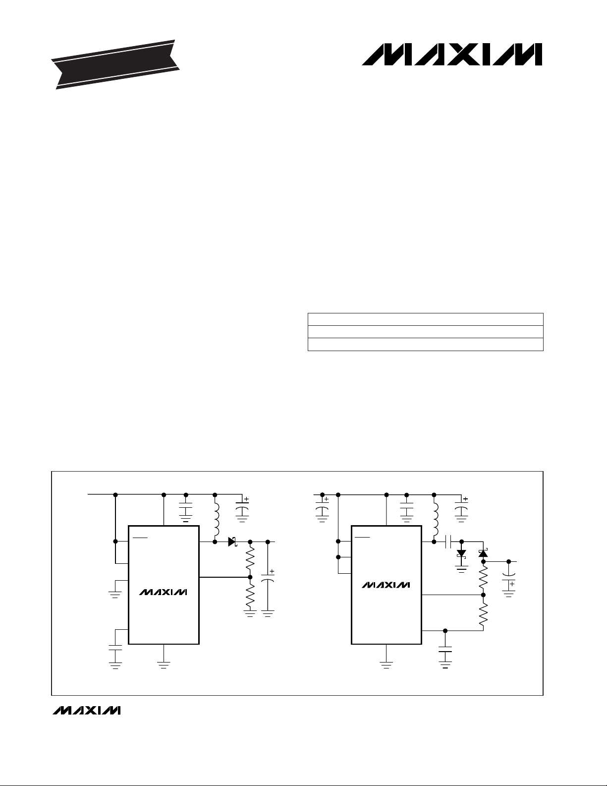
MAX629
SHDN
V
IN
+2.7V
TO +5.5V
LX
V
CC
GND
FB
ISET
POL
REF
POSITIVE OUTPUT VOLTAGE
MAX629
SHDN
-V
OUT
-28V
V
OUT
28V
V
IN
+2.7V
TO +5.5V
LX
V
CC
GND
FB
REF
POL
NEGATIVE OUTPUT VOLTAGE
ISET
___________________________________________________Typical Operating Circuit
19-1219; Rev 1; 6/97
PART TEMP. RANGE PIN-PACKAGE
______________Ordering Information
For free samples & the latest literature: http://www.maxim-ic.com, or phone 1-800-998-8800
Note: To order tape-and-reel shipping, add “-T” to the end of
the part number.
*
Dice are tested at TA= +25°C, DC parameters only.
Pin Configuration appears at end of data sheet.
MAX629C/D 0°C to +70°C Dice*
MAX629ESA -40°C to +85°C 8 SO
EVALUATION KIT MANUAL
AVAILABLE

MAX629
28V, Low-Power, High-Voltage,
Boost or Inverting DC-DC Converter
2 _______________________________________________________________________________________
ABSOLUTE MAXIMUM RATINGS
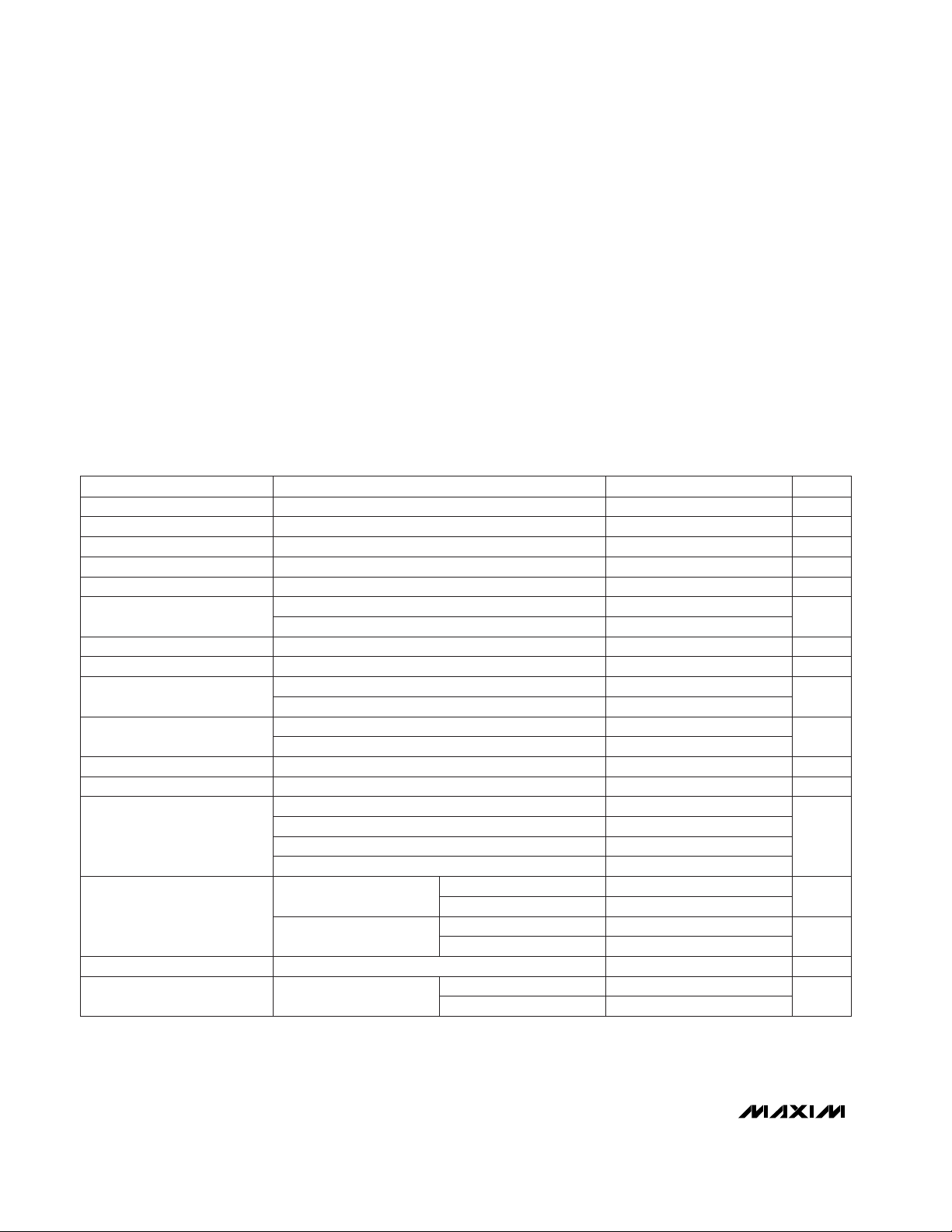
ELECTRICAL CHARACTERISTICS
(VCC= +5V, C
REF
= 0.1µF, TA= -40°C to +85°C, unless otherwise noted. Typical values are at TA= +25°C.) (Note1)
Stresses beyond those listed under “Absolute Maximum Ratings” may cause permanent damage to the device. These are stress ratings only, and functional
operation of the device at these or any other conditions beyond those indicated in the operational sections of the specifications is not implied. Exposure to
absolute maximum rating conditions for extended periods may affect device reliability.
Supply Voltage (VCCto GND)..................................-0.3V to +6V
SHDN to GND...........................................................-0.3V to +6V
ISET, REF, FB, POL to GND.......................-0.3V to (V
CC
+ 0.3V)
LX to GND ..............................................................-0.3V to +30V
Continuous Power Dissipation (T
A
= +70°C)
SO (derate 5.88mW/°C above +70°C)..........................471mW
Operating Temperature Range ...........................-40°C to +85°C
Junction Temperature......................................................+150°C
Storage Temperature Range.............................-65°C to +165°C
Lead Temperature (soldering, 10sec).............................+300°C
CONDITIONS
V2.7 5.5VCCInput Voltage (Note 2)
UNITSMIN TYP MAXPARAMETER
VFB= 1.3V µA80 120VCCSupply Current
100mV hysteresis V2.3 2.5 2.65VCCUndervoltage Lockout
SHDN = GND
µA0.04 1VCCShutdown Current
A
0.39 0.45 0.51
Circuit of Figure 2
VLX= 28V, TA= +85°C µA0.05 2.5LX Leakage Current
POL = GND
µs
0.7 1.0 1.3
Minimum LX Off-Time
µs6.5 8.5 10.0Maximum LX On-Time
0.20 0.25 0.33
LX Switch-Current Limit
V28Positive Output Voltage
POL = GND, VFB< 1V 3.0 4.5 6.0
POL = V
CC
2.0 3.2 3.8
POL = GND
(positive output)
V
1.218 1.282
1.225 1.250 1.275
nA5 50FB Input Bias Current
1.225 1.250 1.275
VCC= 5V
Ω
0.6 1.2
VCC= 3.3V 0.7 1.4
LX On-Resistance
TA= 0°C to +85°C
TA= -40°C to +85°C
TA= 0°C to +85°C
TA= -40°C to +85°C
POL = V
CC
(negative output)
mV
-25 25
FB Set Point
-15 0 15
VCC= 2.7V to 5.5V,
no load on REF
V
1.218 1.282
REF Output Voltage
TA= 0°C to +85°C
TA= -40°C to +85°C
V
IH
V
2.4
SHDN, POL, ISET Logic Levels
V
IL
0.4
Voltage applied to L1 (VIN) V
0.8
V
OUT
Input Supply Voltage (Note 2)
Circuit of Figure 3 V
-V
IN
-28
Negative Output Voltage
ISET = V
CC
ISET = GND
POL = V
CC, VFB
> 0.25V 3.0 4.5 6.0

MAX629
28V, Low-Power, High-Voltage,
Boost or Inverting DC-DC Converter
_______________________________________________________________________________________ 3
ELECTRICAL CHARACTERISTICS (continued)
(VCC= +5V, C
REF
= 0.1µF, TA= -40°C to +85°C, unless otherwise noted. Typical values are at TA= +25°C.) (Note 1)
Note 1: Specifications to -40°C are guaranteed by design and not production tested.
Note 2: The IC itself requires a supply voltage between +2.7V and +5.5V; however, the voltage that supplies power to the inductor
can vary from 0.8V to 28V, depending on circuit operating conditions.
Note 3: For reference currents less than 10µA, a 0.1µF reference-bypass capacitor is adequate.
Circuit of Figure 2, V
OUT
= 24V, VCC= 3V to 5.5V,
I
LOAD
= 5mA
%/V0.2Line Regulation
Die temperature °C150
I
REF
= 0µA to 100µA, C
REF
= 0.47µF (Note 3)
Thermal Shutdown Threshold
Circuit of Figure 2, V
OUT
= 24V, VCC= 5V,
I
LOAD
= 0mA to 5mA
%0.15Load Regulation
CONDITIONS
mV10 25REF Load Regulation
UNITSMIN TYP MAXPARAMETER
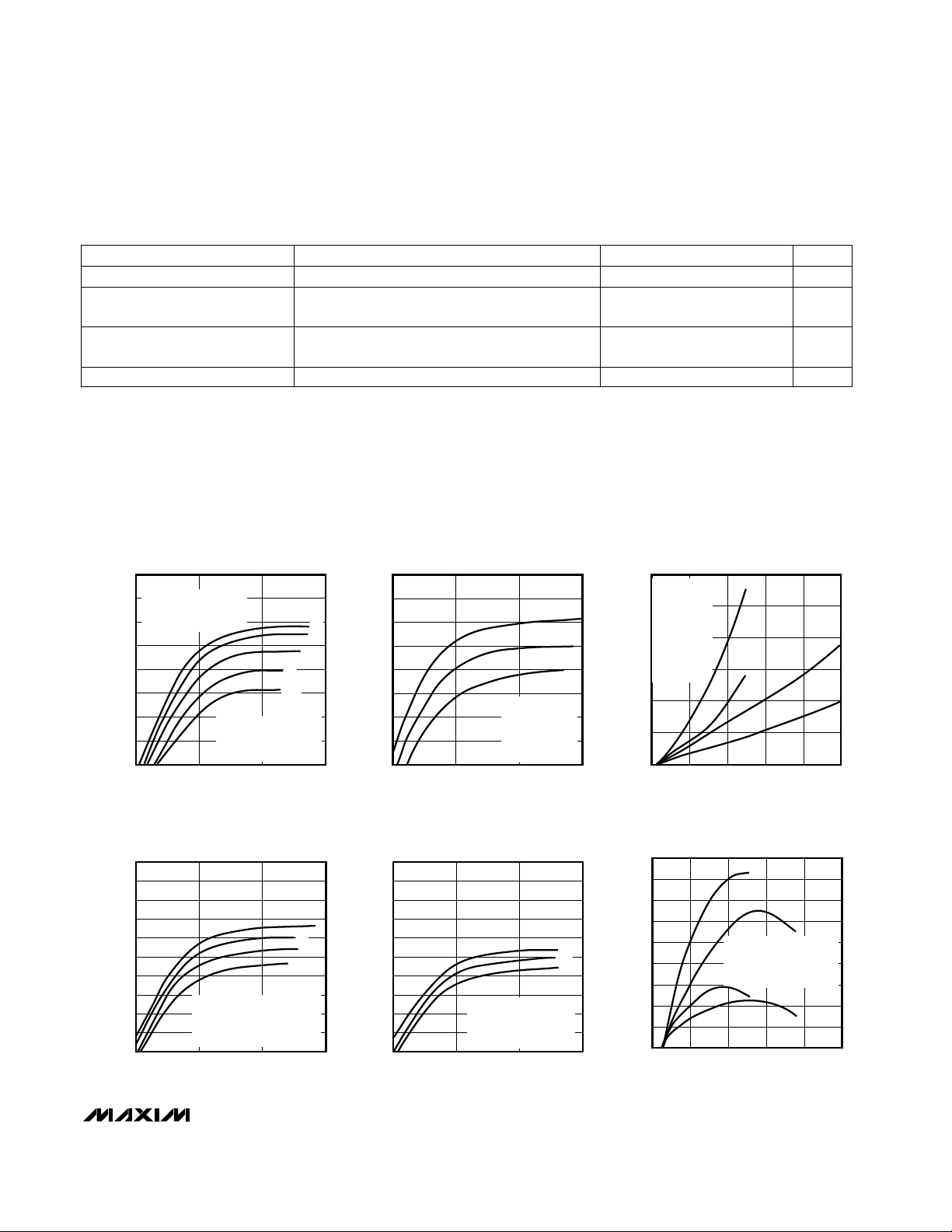
__________________________________________Typical Operating Characteristics
(SHDN = VCC, C
REF
= 0.1µF, TA= +25°C, unless otherwise noted.)
100
60
0.1 100
EFFICIENCY vs. LOAD CURRENT
(V
OUT
= +24V)
65
70
95
90
85
MAX629-01
LOAD CURRENT (mA)
EFFICIENCY (%)
1 10
80
75
D
D: VIN = 5V, ISET = GND
E: V
IN
= 3V, ISET = V
CC
F: VIN = 3V, ISET = GND
V
OUT
= 24V
A: V
IN
= 12V, ISET = V
CC
B: VIN = 12V, ISET = GND
C: V
IN
= 5V, ISET = V
CC
E, F
C
B
A
100
60
0.1 100
EFFICIENCY vs. LOAD CURRENT
(V
OUT
= +12V)
70
65
95
85
90
MAX629-02
LOAD CURRENT (mA)
EFFICIENCY (%)
1 10
80
75
C
B
A
V
OUT
= 12V,
ISET = V
CC
or GND
A: V
IN
= 9V
B: V
IN
= 5V
C: V
IN
= 3V
300
0
0 20
MAXIMUM LOAD CURRENT vs.
INPUT VOLTAGE (V
OUT
= +24V, +12V)
50
250
200
MAX629-03
INPUT VOLTAGE (V)
MAXIMUM LOAD CURRENT (mA)
8 124 16
150
100
A
B
C
D
A: V
OUT
= 12V,
ISET = V
CC
B: V
OUT
= 12V,
ISET = GND
C: V
OUT
=24V,
ISET = V
CC
D: V
OUT
= 24V,
ISET = GND
100
50
0.1 100
EFFICIENCY vs. LOAD CURRENT
(V
OUT
= -18V)
65
60
55
95
80
85
90
MAX629-04
LOAD CURRENT (mA)
EFFICIENCY (%)
1 10
75
70
C
A
A: VIN = 12V, ISET = V
CC
B: VIN = 12V, ISET = GND
C: V
IN
= 5V, ISET = VCC or GND
D: V
IN
= 3V, ISET = VCC or GND
B
D
100
50
0.1 100
EFFICIENCY vs. LOAD CURRENT
(V
OUT
= -12V)
65
60
55
95
80
85
90
MAX629-05
LOAD CURRENT (mA)
EFFICIENCY (%)
1 10
75
70
A
A = VIN = 5V, ISET = V
CC
B = VIN = 5V, ISET = GND
C = V
IN
= 3V, ISET = VCC
D = V
IN
= 3V, ISET = GND
D
B, C
90
0
0 20
MAXIMUM LOAD CURRENT vs. INPUT VOLTAGE
(V
OUT
= -18V, -12V)
30
20
10
80
60
70
MAX629-06
INPUT VOLTAGE (V)
MAXIMUM LOAD CURRENT (mA)
4 8 12 16
50
40
C
A
A: V
OUT
= -12V, ISET = V
CC
B: V
OUT
= -18V, ISET = V
CC
C: V
OUT
= -12V, ISET = GND
D: V
OUT
= -18V, ISET = GND
D
B

MAX629
28V, Low-Power, High-Voltage,
Boost or Inverting DC-DC Converter
4 _______________________________________________________________________________________
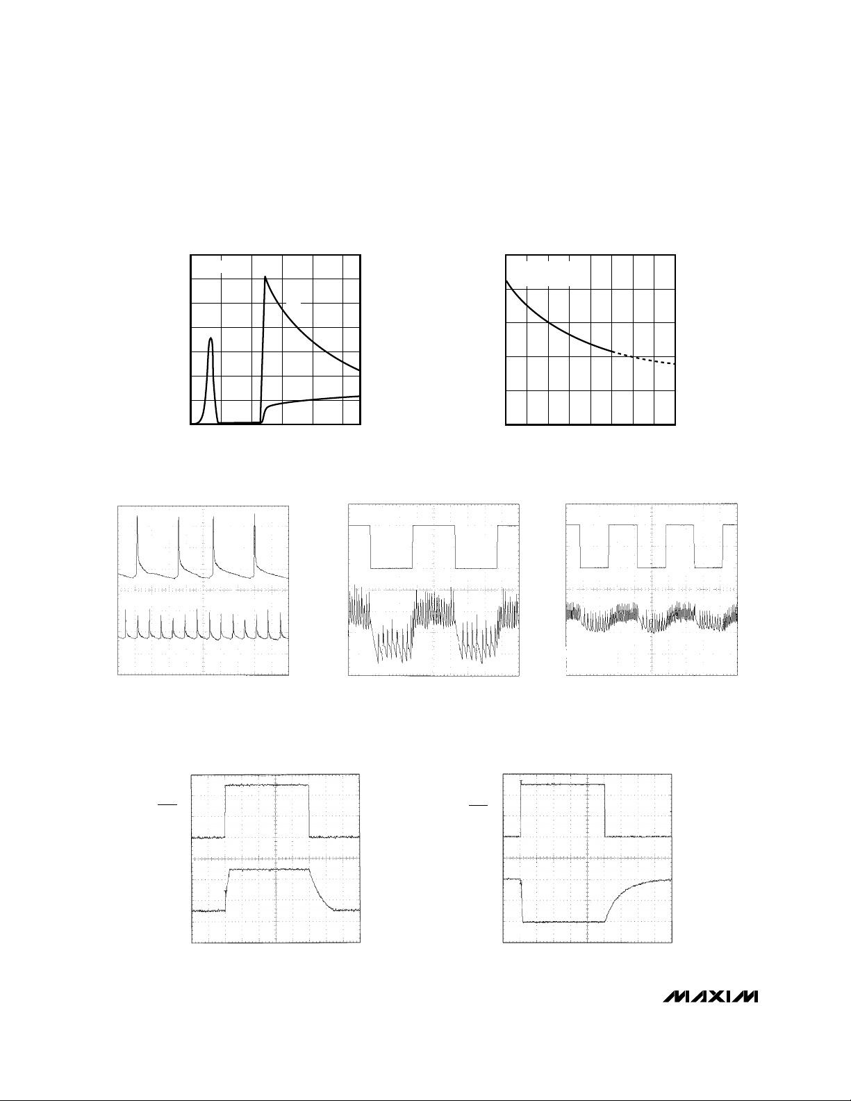
700
600
0
0 1
SUPPLY CURRENT
vs. INPUT VOLTAGE
500
400
300
100
MAX629-07
INPUT VOLTAGE (V)
SUPPLY CURRENT (µA)
2 3 4 5
200
VIN = V
CC
I
CC
I
IN
I
IN
1.255
1.250
1.230
0 20 40
REFERENCE VOLTAGE
vs. REFERENCE LOAD CURRENT
1.245
1.240
MAX629-08
REFERENCE LOAD CURRENT (µA)
REFERENCE VOLTAGE (V)
60 80 100 120 140 160
1.235
VIN = V
CC
= 5V
C4 = 0.47µF
OUTPUT VOLTAGE RIPPLE
MAX629-09
V
OUT
= +24V, I
LOAD
= 5mA
A: ISET = V
CC
, 20mV/div
B: ISET = GND, 20mV/div
A
B
10µs/div
SHUTDOWN TRANSIENT
(POSITIVE CONFIGURATION)
MAX629-12
VCC = VIN = 5V, RL = 4kΩ
50ms/div
5V
SHDN
0V
24V
V
OUT
0V
LOAD-TRANSIENT RESPONSE
(I
SET
= VCC, I
LIM
= 500mA)
MAX629-10
V
OUT
= +24V, ISET = V
CC
A: LOAD CURRENT, 0mA TO 5mA, 2.5mA/div
B: V
OUT,
AC-COUPLED, 10mV/div
A
5mA
0mA
B
200µs/div
LOAD-TRANSIENT RESPONSE
(I
SET
= GND, I
LIM
= 250mA)
MAX629-11
V
OUT
= +24V, ISET = GND
A: LOAD CURRENT, 0mA TO 5mA, 2.5mA/div
B: V
OUT,
AC-COUPLED, 10mV/div
A
0mA
5mA
B
100µs/div
SHUTDOWN TRANSIENT
(NEGATIVE CONFIGURATION)
MAX629-13
START-UP DELAY, VCC = VIN = 5V, I
LOAD
= 5mA
20ms/div
VCC = VIN = 5V, RL = 4kΩ
50ms/div
5V
0V
0V
V
OUT
-20V
SHDN
____________________________Typical Operating Characteristics (continued)
(SHDN = VCC, C
REF
= 0.1µF, TA= +25°C, unless otherwise noted.)
 Loading...