

General Description
The MAX6220 is a low-noise, precision voltage reference with extremely low 20ppm/°C temperature coefficient over the automotive temperature range (-40°C to
+125°C) and excellent ±0.1% initial accuracy. This
device features buried-zener technology for low noise
performance. The load-regulation specification is guaranteed for source and sink currents up to 15mA.
Excellent line and load regulation and low output
impedance at high frequency make the MAX6220 ideal
for high-resolution data-conversion systems up to
16 bits. The MAX6220 is set for 2.5V, 4.096V, and
5.0V outputs.
Applications
High-Accuracy Industrial and Process Control
ATE Equipment
Precision Current Sources
Features
♦ Low 20ppm/°C Temperature Coefficient over
-40°C to +125°C Range
♦ Very Low 1.5µVp-p Noise (0.1Hz to 10Hz)
♦ ±0.1% Initial Accuracy
♦ ±15mA Output Source and Sink Current
♦ 8V to 40V Input Voltage Range
♦ Optional Noise Reduction and Voltage Trim
♦ Excellent Transient Response
♦ Low 20ppm/1000hr Long-Term Stability
♦ Stable for All Capacitive Loads
MAX6220
Low-Noise, Precision, +2.5V/+4.096V/+5V
Voltage Reference
________________________________________________________________ Maxim Integrated Products 1
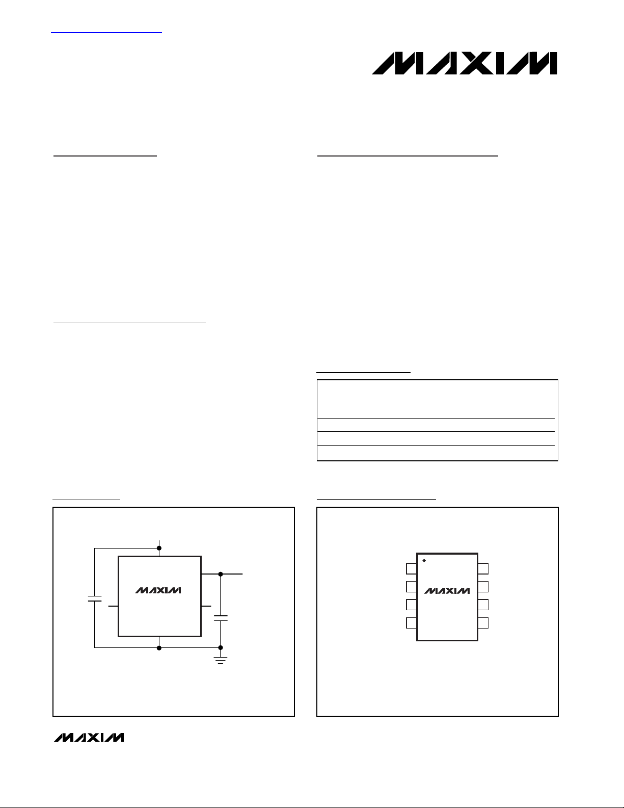
Typical Operating Circuit
OUT
NR
TRIM
GND
I.C.
I.C.
IN
I.C.
SOIC
TOP VIEW
1
2
8
7
3
4
6
5
MAX6220
Pin Configuration
19-1930; Rev 0; 4/01
PART
TEMP. RANGE
PIN-
OUPUT
(V)
MAX6220ASA25
8 SO 2.5
MAX6220ASA41
8 SO 4.096
MAX6220ASA50
8 SO 5.0
For pricing, delivery, and ordering information, please contact Maxim/Dallas Direct! at
1-888-629-4642, or visit Maxim’s website at www.maxim-ic.com.
Ordering Information
查询MAX6220供应商
PACKAGE
VOLTAGE
8V TO 40V INPUT
IN
OUT
*
2.2µF
*OPTIONAL (STABLE WITH ALL CAPACITIVE LOADS)
NR
MAX6220
GND
TRIM
REFERENCE OUT
*
2.2µF
-40°C to +125°C
-40°C to +125°C
-40°C to +125°C
MAX6220
Low-Noise, Precision, +2.5V/+4.096V/+5V
Voltage Reference
2 _______________________________________________________________________________________
ABSOLUTE MAXIMUM RATINGS
ELECTRICAL CHARACTERISTICS—(+2.5V)
(VIN= +10V, I
OUT
= 0mA, TA= T
MIN
to T
MAX
, unless otherwise noted. Typical values are at TA= +25°C.)
Stresses beyond those listed under “Absolute Maximum Ratings” may cause permanent damage to the device. These are stress ratings only, and functional
operation of the device at these or any other conditions beyond those indicated in the operational sections of the specifications is not implied. Exposure to
absolute maximum rating conditions for extended periods may affect device reliability.
(Voltages Referenced to GND)
IN..............................................................................-0.3V to +42V
OUT, TRIM ...............................................................-0.3V to +12V
NR ..............................................................................-0.3V to +6V
OUT Short-Circuit to GND Duration (V
IN
≤ 12V)..........Continuous
OUT Short-Circuit to GND Duration (V
IN
≤ 42V) ........................5s
OUT Short-Circuit to IN Duration (V
IN
≤ 12V) ..............Continuous
Continuous Power Dissipation (T
A
= +70°C)
8-Pin SO (derate 5.9mW/°C above +70°C) ....................471mW
Operating Temperature Range...........................-40°C to +125°C
Storage Temperature Range ..............................-65°C to +150°C
Lead Temperature (soldering, 10s)...................................+300°C
PARAMETER
SYMBOL
CONDITIONS T
A
MIN
TYP
MAX
UNITS
Input Voltage Range V
IN
840V
Output Voltage V
OUT
V
Output Voltage Temperature
Coefficient (Note 1)
220
ppm/˚C
27
Line Regulation (Note 2)
∆V
IN
8V ≤ VIN ≥ 40V
45
ppm/V
16
Sourcing: 0mA ≤ I
OUT
≤ 15mA
15
16
Load Regulation (Note 2)
∆V
OUT
/
Sinking: -15mA ≤ I
OUT
≤ 0mA
30
ppm/mA
2.9
Supply Current I
IN
3.3
mA
Trim-Adjustment Range
(Figure 1) ±15
mV
Turn-On Settling Time t
ON
To ±0.01% of final value 5 µs
0.1Hz ≤ f ≥ 10Hz
µVp-p
Output Noise Voltage
(Note 3)
e
N
10Hz ≤ f ≥ 1kHz
2.8
µV
RMS
Temperature Hysteresis (Note 4) 20 ppm
Long-Term Stability
∆t = 1000hr 20 ppm
TCV
+25°C 2.497 2.500 2.503
OUT
∆V
/
OUT
∆I
OUT
∆V
OUT
∆V
OUT
+25°C
+25°C
+25°C
+25°C 1.8
±25
1.5
1.3
MAX6220
Low-Noise, Precision, +2.5V/+4.096V/+5V
Voltage Reference
_______________________________________________________________________________________ 3
ELECTRICAL CHARACTERISTICS—(+4.096V)
(VIN= +10V, I
OUT
= 0mA, TA= T
MIN
to T
MAX
, unless otherwise noted. Typical values are at TA= +25°C.)
PARAMETER
SYMBOL
CONDITIONS T
A
MIN
TYP
MAX
UNITS
Input Voltage Range V
IN
840V
Output Voltage V
OUT
V
Output VoltageTemperature
Coefficient (Note 1)
220
ppm/°C
27
Line Regulation (Note 2)
∆V
IN
8V ≤ VIN ≥ 40V
45
ppm/V
16
Sourcing: 0mA ≤ I
OUT
≤ 15mA
15
16
Load Regulation (Note 2)
∆V
OUT
/
Sinking: -15mA ≤ I
OUT
≤ 0mA
30
ppm/mA
1.9 3.1
Supply Current I
IN
3.5
mA
Trim-Adjustment Range
(Figure 1) ±24
mV
Turn-On Settling Time t
ON
To ±0.01% of final value 5 µs
0.1Hz ≤ f ≥ 10Hz 2.4 µVp-p
Output Noise Voltage
(Note 3)
e
N
10Hz ≤ f ≥ 1kHz 2.0 4.0 µV
RMS
Temperature Hysteresis (Note 4) 20 ppm
Long-Term Stability
∆t = 1000hr 20 ppm
TCV
∆V
∆I
∆V
∆V
OUT
/
OUT
OUT
OUT
OUT
+25°C 4.092 4.096 4.100
+25°C
+25°C
+25°C
+25°C
±40

MAX6220
Low-Noise, Precision, +2.5V/+4.096V/+5V
Voltage Reference
4 _______________________________________________________________________________________
ELECTRICAL CHARACTERISTICS—(+5.0V)
(VIN= +10V, I
OUT
= 0mA, TA= T
MIN
to T
MAX
, unless otherwise noted. Typical values are at TA= +25°C.)
Note 1: Temperature coefficient is measured by the box method; i.e., the maximum ∆V
OUT
is divided by ∆T x V
OUT
.
Note 2: Line regulation (∆V
OUT
/ (V
OUT
x ∆VIN)) and load regulation (∆V
OUT
/ (V
OUT
x ∆I
OUT
)) are measured with pulses and do
not include output voltage changes due to die-temperature changes.
Note 3: Noise specifications are guaranteed by design.
Note 4: Temperature hysteresis is specified at T
A
= +25°C by measuring V
OUT
before and after changing temperature by +25°C.
PARAMETER
SYMBOL
CONDITIONS T
A
MIN
TYP
MAX
UNITS
Input Voltage Range V
IN
840V
Output Voltage V
OUT
V
Output Voltage Temperature
Coefficient (Note 1)
220
27
Line Regulation (Note 2)
∆V
IN
8V ≤ VIN ≥ 40V
45
ppm/V
16
Sourcing: 0mA ≤ I
OUT
≤ 15mA
15
16
Load Regulation (Note 2)
∆V
OUT
/
Sinking: -15mA ≤ I
OUT
≤ 0mA
30
2.0 3.3
Supply Current I
IN
3.7
mA
Trim-Adjustment Range
(Figure 1) ±30
mV
Turn-On Settling Time t
ON
To ±0.01% of final value 5 µs
0.1Hz ≤ f ≥ 10Hz 3.0 µVp-p
Output Noise Voltage
(Note 3)
e
N
10Hz ≤ f ≥ 1kHz 2.5 5.0 µV
RMS
Temperature Hysteresis (Note 4) 20 ppm
Long-Term Stability
∆t = 1000hr 20 ppm
+25°C 4.995 5.000 5.005
TCV
OUT
∆V
/
∆I
∆V
∆V
OUT
OUT
OUT
OUT
+25°C
+25°C
+25°C
+25°C
±50
ppm/°C
ppm/mA

Low-Noise, Precision, +2.5V/+4.096V/+5V
Voltage Reference
MAX6220
_______________________________________________________________________________________ 5
Typical Operating Characteristics
(VIN= +10V, I
OUT
= 0mA, TA = +25°C, unless otherwise noted.)
2.0
-1.5
-55 -15 65
MAX6220_50
NORMALIZED OUTPUT VOLTAGE
vs. TEMPERATURE
-1.0
1.0
MAX6220
toc01
TEMPERATURE (°C)
∆V
OUT
(mV)
∆V
OUT
(ppm)
25 105-35 5 8545 125
0.5
0
-0.5
1.5
400
-300
-200
200
100
0
-100
300
-20
-10
0
10
20
30
40
50
60
0 5 10 15 20 25 30 35 40
CHANGE IN OUTPUT VOLTAGE
vs. INPUT VOLTAGE
V
IN
(V)
∆V
OUT
(ppm)
MAX6220
toc07
-55 -15 65
MAX6220_41
NORMALIZED OUTPUT VOLTAGE
vs. TEMPERATURE
-1.0
1.0
MAX6220
toc02
TEMPERATURE (°C)
∆V
OUT
(mV)
∆V
OUT
(ppm)
25 105-35 5 8545 125
0.5
0
-0.5
1.5
-250
-125
0
125
250
375
-0.4
-0.3
-0.2
-0.1
00
0.1
0.2
0.3
0.4
0.5
0.6
0.7
-160
-120
-80
-40
40
80
120
160
200
240
280
-55 -15 65
MAX6220_25
NORMALIZED OUTPUT VOLTAGE
vs. TEMPERATURE
MAX6220
toc03
TEMPERATURE (°C)
∆V
OUT
(mV)
∆V
OUT
(ppm)
25 105-35 5 8545 125
-250
-200
-150
-100
-50
0
50
100
150
200
-40 -30 -20 -10 0 10 20 30 40
MAX6220_25
CHANGE IN OUTPUT VOLTAGE
vs. OUTPUT CURRENT
MAX6220
toc06
I
OUT
(mA)
∆V
OUT
(µV)
TA = +85°C
TA = -40°C
TA = +25°C
-300
-200
-100
0
100
200
300
-40 -30 -20 -10 0 10 20 30 40
MAX6220_41
CHANGE IN OUTPUT VOLTAGE
vs. OUTPUT CURRENT
MAX6220
toc05
I
OUT
(mA)
∆V
OUT
(µV)
TA = +25°C
T
A
= -40°C
T
A
= +85°C
-400
-300
-200
-100
0
100
200
300
-40 -30 -20 -10 0 10 20 30 40
MAX6220_50
CHANGE IN OUTPUT VOLTAGE
vs. OUTPUT CURRENT
MAX6220
toc04
I
OUT
(mA)
∆V
OUT
(µV)
TA = +25°C
TA = -40°C
TA = +85°C
1.0
1.2
1.4
1.6
1.8
2.0
2.2
2.4
2.6
2.8
3.0
0 5 10 15 20 25 30 35 40
SUPPLY CURRENT vs. SUPPLY VOLTAGE
MAX6220
toc08
SUPPLY VOLTAGE (V)
SUPPLY CURRENT (mA)
MAX6220_25
MAX6220_41
MAX6220_50
1.0
1.5
2.0
2.5
3.0
3.5
-55 -35 -15 5 25 45 65 85 105 125
SUPPLY CURRENT vs. TEMPERATURE
MAX6220
toc09
TEMPERATURE (°C)
SUPPLY CURRENT (mA)
MAX6220_41
MAX6220_50
MAX6220_25

MAX6220
Low-Noise, Precision, +2.5V/+4.096V/+5V
Voltage Reference
6 _______________________________________________________________________________________
Typical Operating Characteristics (continued)
(VIN= +10V, I
OUT
= 0mA, TA = +25°C, unless otherwise noted.)
MAX6220_41
0.1Hz TO 10Hz NOISE
V
OUT
, 1µV/div
MAX6220
toc14
1s/div
C
OUT
= CNR = 0µF
0
5
10
15
20
25
30
35
40
45
50
10 100 1k 10k
MAX6220_25
OUTPUT NOISE-VOLTAGE
DENSITY vs. FREQUENCY
MAX6220
toc10
FREQUENCY (Hz)
CNR = 0µF
CNR = 1µF
OUTPUT NOISE DENSITY (nV/√ Hz)
MAX6220_25
0.1Hz TO 10Hz NOISE
V
OUT
, 0.5µV/div
MAX6220
toc13
1s/div
C
OUT
= CNR = 0µF
0
10
20
30
40
50
60
70
80
90
10 100 1k 10k
MAX6220_41
OUTPUT NOISE-VOLTAGE
DENSITY vs. FREQUENCY
MAX6220
toc11
FREQUENCY (Hz)
CNR = 0µF
CNR = 1µF
OUTPUT NOISE DENSITY (nV/√ Hz)
0
10
20
30
40
50
60
70
80
100
90
10 100 1k 10k
MAX6220_50
OUTPUT NOISE-VOLTAGE
DENSITY vs. FREQUENCY
MAX6220
toc12
FREQUENCY (Hz)
CNR = 0µF
CNR = 1µF
OUTPUT NOISE DENSITY (nV√ Hz)
MAX6220_50
0.1Hz TO 10Hz NOISE
V
OUT
, 1µV/div
1s/div
C
OUT
= CNR = 0µF
MAX6220
toc15
10 1M10k
FREQUENCY (Hz)
100 1k 100k
100
0.01
OUTPUT IMPEDANCE vs. FREQUENCY
0.1
MAX6220
toc16
OUTPUT IMPEDANCE (Ω)
1
10
I
SINK
= 5mA
I
SOURCE
= 5mA
60
70
80
90
100
110
120
10 100 1k 10k
RIPPLE REJECTION
vs. FREQUENCY (C
NR
= 1µF)
MAX6220
toc17
FREQUENCY (Hz)
RIPPLE REJECTION (dB)
MAX6220_41
MAX6220_25
MAX6220_50
60
65
70
75
80
85
90
95
10 100 1k 10k
RIPPLE REJECTION
vs. FREQUENCY (C
NR
= 0µF)
MAX6220
toc18
FREQUENCY (Hz)
RIPPLE REJECTION (dB)
MAX6220_25
MAX6220_41
MAX6220_50

MAX6220
Low-Noise, Precision, +2.5V/+4.096V/+5V
Voltage Reference
_______________________________________________________________________________________ 7
Typical Operating Characteristics (continued)
(VIN= +10V, I
OUT
= 0mA, TA = +25°C, unless otherwise noted.)
2µs/div
MAX6220_50
LOAD-TRANSIENT RESPONSE (SOURCING)
B
A
A: I
OUT
, 10mA/div (SOURCING)
B: V
OUT
, 500µV/div
MAX6220
toc19
0mA
-10mA
2µs/div
MAX6220_50
LOAD-TRANSIENT RESPONSE (SINKING)
B
A
0mA
10mA
A: I
OUT
, 10mA/div (SINKING)
B: V
OUT
, 500µV/div
MAX6220
toc20
1µs/div
MAX6220_50
LOAD-TRANSIENT RESPONSE
B
A
A: I
OUT
(±10mA SOURCE AND SINK), 20mA/div, AC COUPLED
B: V
OUT
, 20mV/div, AC COUPLED
MAX6220
toc21
-10mA
+10mA
VIN = 10V
C
OUT
= CNR = 0µF
1µs/div
MAX6220_25
TURN-ON AND TURN-OFF TRANSIENT RESPONSE
B
A
A: VIN, 10V/div
B: V
OUT
, 1V/div
MAX6220
toc22
+10V
0
CIN = C
OUT
= CNR = 0µF
1µs/div
MAX6220_41
TURN-ON AND TURN-OFF TRANSIENT RESPONSE
B
A
A: VIN, 10V/div
B: V
OUT
, 1V/div
MAX6220
toc22
+10V
0
CIN = C
OUT
= CNR = 0µF
1µs/div
MAX6220_50
TURN-ON AND TURN-OFF TRANSIENT RESPONSE
B
A
A: VIN, 10V/div
B: V
OUT
, 1V/div
MAX6220
toc24
+10V
0
CIN = C
OUT
= CNR = 0µF

MAX6220
Low-Noise, Precision, +2.5V/+4.096V/+5V
Voltage Reference
8 _______________________________________________________________________________________
Detailed Description
Temperature Stability
The MAX6220 is a highly stable, low-noise voltage reference that uses a low-power temperature-compensation scheme to achieve laboratory-standard temperature stability. This produces a nearly flat temperature
curve, yet does not require the power associated with
heated references.
The output voltage can be trimmed 0.6% (min) by connecting a 10kΩ potentiometer between OUT and GND,
and connecting its tap to the TRIM pin (Figure 1). The
external trimming does not affect temperature stability.
Noise Reduction
To augment wideband noise reduction, add a 1µF
capacitor to the NR pin (Figure 2). Larger values do not
improve noise appreciably (see Typical Operating
Characteristics).
Noise in the power-supply input can affect output
noise, but can be reduced by adding an optional
bypass capacitor to the IN pin and GND.
Bypassing
The MAX6220 is stable with capacitive load values from
0µF to 100µF, for all values of load current. Adding an
output bypass capacitor can help reduce noise and
output glitching caused by load transients.
Applications Information
Negative Regulator
Figure 3 shows how both a +5V and -5V precision reference can be obtained from a single unregulated +5V
supply. The MAX865 generates approximately ±9V to
operate both the MAX6220 reference and the MAX480
inverting amplifier. The +5V is inverted by the MAX480.
Resistor R1 is optional, and may be used to trim the
±5V references. R2 and R4 should be matched, both in
absolute resistance and temperature coefficient. R3 is
optional, and is adjusted to set the -5V reference.
_____________________Pin Description
NAME FUNCTION
1, 7, 8 I.C.
Internally Connected. Do not use.
2 IN Positive Power-Supply Input
PIN
4 GND Ground
3 NR
Noise Reduction. Optional capacitor
connection for wideband noise
reduction. Leave open if not used
(Figure 2).
6 OUT Voltage Reference Output
5 TRIM
External Trim Input. Allows ±1%
output adjustment (Figure 1).
Leave open if not used.
MAX6220
IN
8V TO 40V INPUT
REFERENCE OUT
OUT
TRIM
10kΩ
NR
GND
MAX6220
IN
8V TO 40V INPUT
REFERENCE OUT
OUT
TRIM
NR
*OPTIONAL
1µF
GND
2.2µF*
Figure 1. Output Voltage Adjustment Figure 2. Noise-Reduction Capacitor

MAX6220
Low-Noise, Precision, +2.5V/+4.096V/+5V
Voltage Reference
_______________________________________________________________________________________ 9
Figure 3. +5V and -5V References from a Single +5V Supply
Chip Information
TRANSISTOR COUNT: 435
+5V INPUT
VCCV+
3.3µF
C1+
C1-
IN
MAX865
3.3µF
C2+
C2-
2.2µF
GND
C1
2.2µF
V-
C2
1µF
NR
MAX6220
GND
OUT
TRIM
R1
10kΩ
C3
2.2µF
+REFERENCE OUT
R2
100kΩ
R3
1kΩ
MAX480
R4
100kΩ
-REFERENCE OUT
MAX6220
Maxim cannot assume responsibility for use of any circuitry other than circuitry entirely embodied in a Maxim product. No circuit patent licenses are
implied. Maxim reserves the right to change the circuitry and specifications without notice at any time.
10 __________________Maxim Integrated Products, 120 San Gabriel Drive, Sunnyvale, CA 94086 (408) 737-7600
© 2001 Maxim Integrated Products Printed USA is a registered trademark of Maxim Integrated Products.
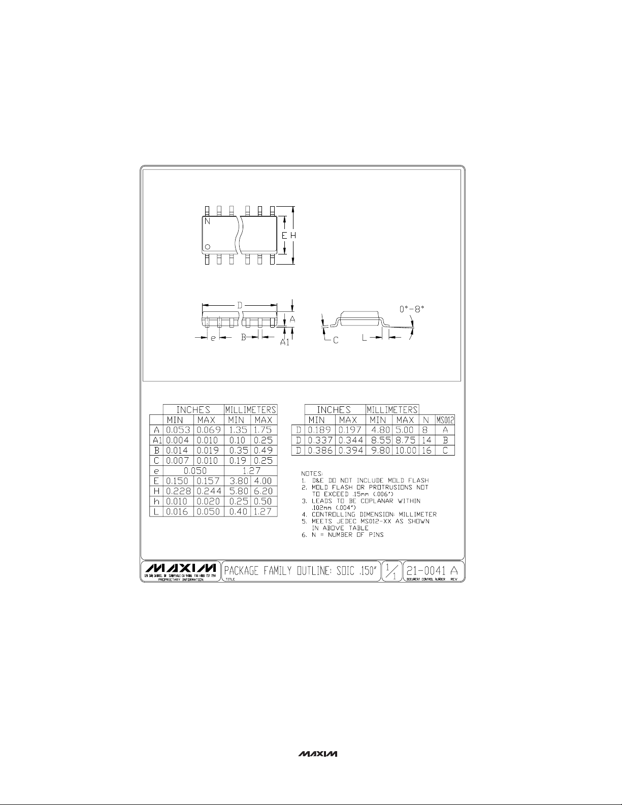
________________________________________________________Package Information
Low-Noise, Precision, +2.5V/+4.096V/+5V
Voltage Reference
SOICN.EPS
 Loading...