

General Description
The MAX6190–MAX6195/MAX6198 precision, micropower, low-dropout voltage references offer high initial
accuracy and very low temperature coefficient through
a proprietary curvature-correction circuit and lasertrimmed precision thin-film resistors.
These series-mode bandgap references draw a maximum of only 35µA quiescent supply current, making
them ideal for battery-powered instruments. They offer
a supply current that is virtually immune to input voltage variations. Load-regulation specifications are
guaranteed for source and sink currents up to 500µA.
These devices are internally compensated, making
them ideal for applications that require fast settling,
and are stable with capacitive loads up to 2.2nF.
Features
o ±2mV (max) Initial Accuracy
o 5ppm/°C (max) Temperature Coefficient
o 35µA (max) Supply Current
o 100mV Dropout at 500µA Load Current
o 0.12µV/µA Load Regulation
o 8µV/V Line Regulation
Applications
Hand-Held Instruments
Analog-to-Digital and Digital-to-Analog Converters
Industrial Process Control
Precision 3V/5V Systems
Hard-Disk Drives
MAX6190–MAX6195/MAX6198
Precision, Micropower,
Low-Dropout Voltage References
________________________________________________________________
Maxim Integrated Products
1
19-1408; Rev 3; 4/10
Ordering Information
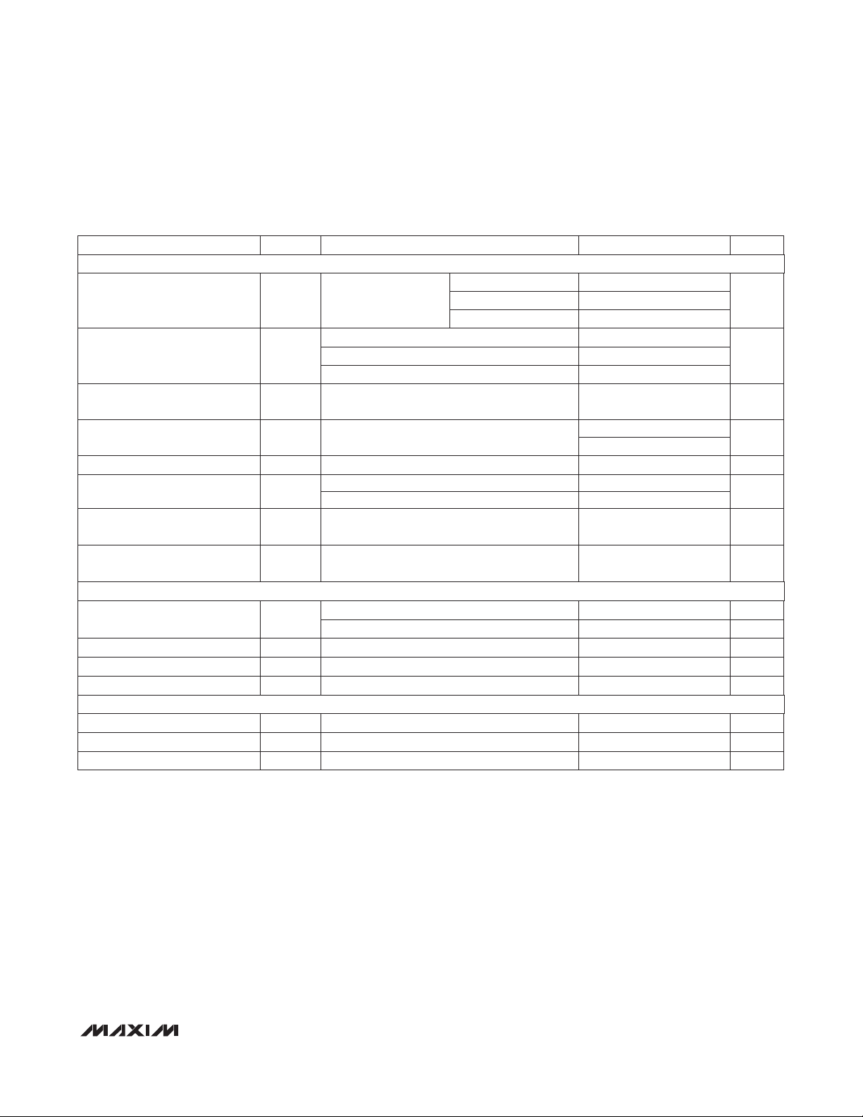
Selector Guide
Typical Operating Circuit appears at end of data sheet.
<25±105.000MAX6195C
<10±55.000MAX6195B
<5±25.000
MAX6195A
<25±104.500MAX6194C
<10±54.500MAX6194B
<5±24.500
MAX6194A
<25±103.000MAX6193C
<10±53.000MAX6193B
<5±23.000
MAX6193A
<25±102.500MAX6192C
<10±52.500MAX6192B
<5±22.500
MAX6192A
TEMPERATURE
COEFFICIENT
(ppm/°C)
<5
<10
<25
<5
<10
<25
PART
OUTPUT
VOLTAGE
(V)
INITIAL
ACCURACY
(mV)
MAX6190B
MAX6190A
1.250 ±2
1.250 ±4
MAX6190C 1.250 ±6
MAX6191B
MAX6191A
2.048 ±2
2.048 ±5
MAX6191C 2.048 ±10
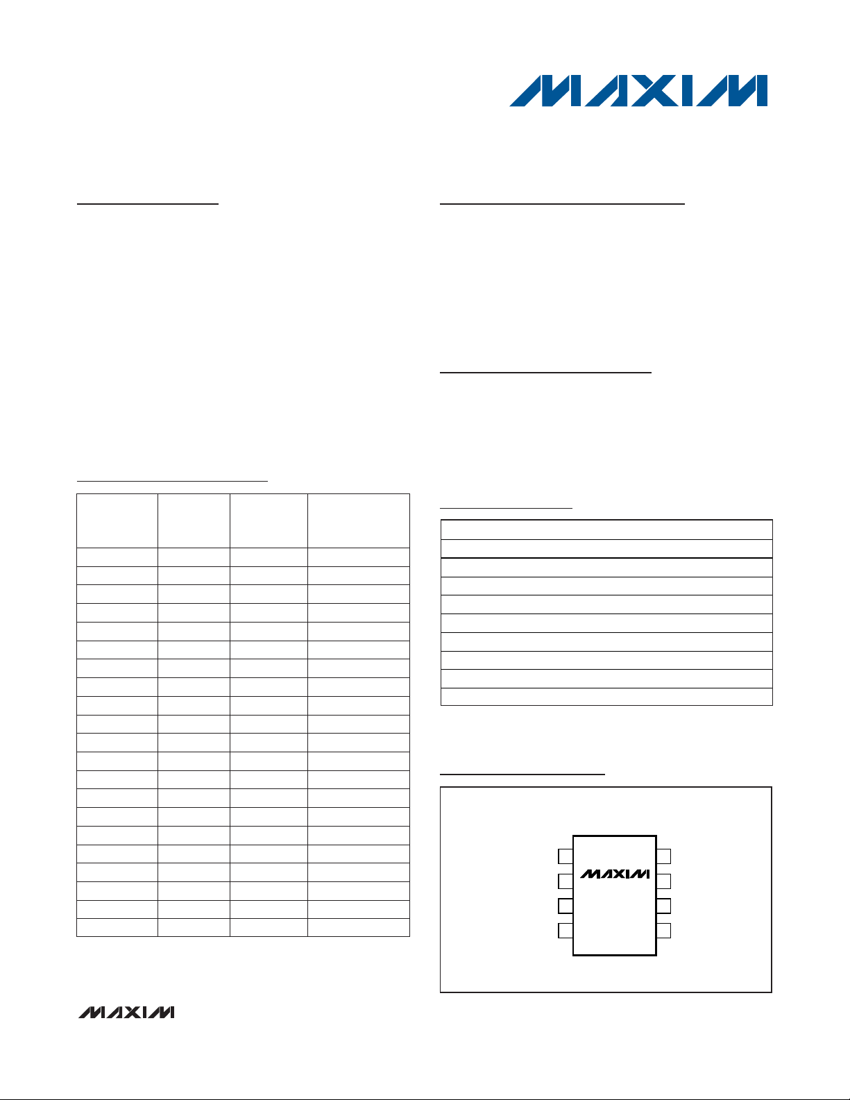
Pin Configuration
For pricing, delivery, and ordering information, please contact Maxim/Dallas Direct! at
1-888-629-4642, or visit Maxim’s website at www.maxim-ic.com.
<25±104.096MAX6198C
<10±54.096MAX6198B
<5±24.096
MAX6198A
Ordering Information continued at end of data sheet.
+
Denotes a lead(Pb)-free /RoHS-compliant package.
PART TEMP RANGE PIN-PACKAGE
MAX6190AESA+ -40°C to +85°C 8 SO
MAX6190BESA+ -40°C to +85°C 8 SO
MAX6190CESA+ -40°C to +85°C 8 SO
MAX6191AESA+ -40°C to +85°C 8 SO
MAX6191BESA+ -40°C to +85°C 8 SO
MAX6191CESA+ -40°C to +85°C 8 SO
MAX6192AESA+ -40°C to +85°C 8 SO
MAX6192BESA+ -40°C to +85°C 8 SO
MAX6192CESA+ -40°C to +85°C 8 SO
TOP VIEW
+
N.C.
N.C.
1
2
3
4
MAX6190–
MAX6195
MAX6198
87N.C.
N.C.IN
OUT
6
N.C.GND
5
SO
MAX6190–MAX6195/MAX6198
Precision, Micropower,
Low-Dropout Voltage References
2 _______________________________________________________________________________________
ABSOLUTE MAXIMUM RATINGS
ELECTRICAL CHARACTERISTICS—MAX6190
(VIN= 5V, I
OUT
= 0nA, TA= T
MIN
to T
MAX
, unless otherwise noted. Typical values are at TA= +25°C.)
Stresses beyond those listed under “Absolute Maximum Ratings” may cause permanent damage to the device. These are stress ratings only, and functional
operation of the device at these or any other conditions beyond those indicated in the operational sections of the specifications is not implied. Exposure to
absolute maximum rating conditions for extended periods may affect device reliability.
Voltages Referenced to GND
IN ......................................................................-0.3V to +13.5V
OUT ..........................................................-0.3V to (V
IN
+ 0.3V)
Output Short Circuit to GND or IN (VIN< 6V) ............Continuous
Output Short Circuit to GND or IN (VIN≥ 6V) .........................60s
Continuous Power Dissipation (TA= +70°C)
8-Pin SO (derate 5.88mW/°C above +70°C)................471mW
Operating Temperature Range ...........................-40°C to +85°C
Junction Temperature......................................................+150°C
Storage Temperature Range .............................-65°C to +150°C
Lead Temperature (soldering, 10s) .................................+300°C
Soldering Temperature (reflow) .......................................+260°C
(Note 3)
TA= +25°C
To 0.1%, C
OUT
= 50pF
VIN= 5V ±100mV, f = 120Hz
10Hz to 10kHz
0.1Hz to 10Hz
1000hrs at +25°C
Sourcing: 0 ≤ I
OUT
≤ 500µA
Short to IN
2.5V ≤ VIN≤ 12.6V
MAX6190A
MAX6190B
Short to GND
MAX6190C
Sinking: -500µA ≤ I
OUT
≤ 0
CONDITIONS
INPUT
nF0 2.2C
OUT
Capacitive-Load Stability Range
µs30t
R
Turn-On Settling Time
dB86V
OUT/VIN
Ripple Rejection
µV
RMS
65
µV
P-P
25
e
OUT
Noise Voltage
DYNAMIC
ppm/
1000hrs
50
∆V
OUT
/
time
Long-Term Stability
ppm75
∆V
OUT
/
cycle
Temperature Hysteresis
(Note 2)
4
mA
4
I
SC
Short-Circuit Current
0.15 0.6
1.246 1.250 1.254
1.248 1.250 1.252
OUTPUT
µV/µA
0.12 0.5
∆V
OUT
/
∆I
OUT
Load Regulation
µV/V880
∆V
OUT
/
∆V
IN
Line Regulation
1.244 1.250 1.256
25
Output-Voltage Temperature
Coefficient (Note 1)
ppm/°C
410
TCV
OUT
UNITSMIN TYP MAXSYMBOLPARAMETER
Supply Voltage Range V
IN
Guaranteed by line-regulation test 2.5 12.6 V
Quiescent Supply Current I
IN
27 35 µA
Change in Supply Current IIN/V
IN
2.5V ≤ VIN≤ 12.6V 0.8 2 µA/V
MAX6190B
MAX6190A
MAX6190C
V
OUT
Output Voltage V
INPUT
DYNAMIC
OUTPUT
825
MAX6190–MAX6195/MAX6198
Precision, Micropower,
Low-Dropout Voltage References
_______________________________________________________________________________________ 3
ELECTRICAL CHARACTERISTICS—MAX6191
(VIN= 5V, I
OUT
= 0nA, TA= T
MIN
to T
MAX
, unless otherwise noted. Typical values are at TA= +25°C.)
V
OUT
(Note 3)
TA= +25°C
To 0.1%, C
OUT
= 50pF
VIN= 5V ±100mV, f = 120Hz
10Hz to 10kHz
0.1Hz to 10Hz
1000hrs at +25°C
Output Voltage
Sourcing: 0 ≤ I
OUT
≤ 500µA
Short to IN
V
2.5V ≤ VIN≤ 12.6V
MAX6191A
MAX6191B
Short to GND
MAX6191C
Sinking: -500µA ≤ I
OUT
≤ 0
CONDITIONS
INPUT
nF0 2.2C
OUT
Capacitive-Load Stability Range
µs30t
R
Turn-On Settling Time
dB84V
OUT/VIN
Ripple Rejection
µV
RMS
105
µV
P-P
40
e
OUT
Noise Voltage
DYNAMIC
ppm/
1000hrs
50
∆V
OUT
/
time
Long-Term Stability
ppm75
∆V
OUT
/
cycle
Temperature Hysteresis
(Note 2)
mA
4
I
SC
Short-Circuit Current
2.043 2.048 2.053
2.046 2.048 2.050
MAX6191B
OUTPUT
MAX6191A
µV/µA
0.12 0.55
∆V
OUT
/
∆I
OUT
Load Regulation
µV/V10 100
∆V
OUT
/
∆V
IN
Line Regulation
2.038 2.048 2.058MAX6191C
Output-Voltage Temperature
Coefficient (Note 1)
ppm/°C
410
TCV
OUT
UNITSMIN TYP MAXSYMBOLPARAMETER
Supply Voltage Range V
IN
Guaranteed by line-regulation test 2.5 12.6 V
Quiescent Supply Current I
IN
27 35 µA
Change in Supply Current IIN/V
IN
2.5V ≤ VIN≤ 12.6V 0.8 2 µA/V
INPUT
DYNAMIC
OUTPUT
825
0.18 0.70
4
25
MAX6190–MAX6195/MAX6198
Precision, Micropower,
Low-Dropout Voltage References
4 _______________________________________________________________________________________
ELECTRICAL CHARACTERISTICS—MAX6192
(VIN= 5V, I
OUT
= 0nA, TA= T
MIN
to T
MAX
, unless otherwise noted. Typical values are at TA= +25°C.)
V
OUT
(Note 3)
TA= +25°C
To 0.1%, C
OUT
= 50pF
VIN= 5V ±100mV, f = 120Hz
10Hz to 10kHz
0.1Hz to 10Hz
1000hrs at +25°C
Output Voltage
Sourcing: 0 ≤ I
OUT
≤ 500µA
Short to IN
V
(V
OUT
+ 0.2V) ≤ VIN≤ 12.6V
MAX6192A
MAX6192B
Short to GND
MAX6192C
Sinking: -500µA ≤ I
OUT
≤ 0
CONDITIONS
INPUT
nF0 2.2C
OUT
Capacitive-Load Stability Range
µs85t
R
Turn-On Settling Time
dB82V
OUT/VIN
Ripple Rejection
µV
RMS
125
µV
P-P
60
e
OUT
Noise Voltage
DYNAMIC
ppm/
1000hrs
50
∆V
OUT
/
time
Long-Term Stability
ppm75
∆V
OUT
/
cycle
Temperature Hysteresis
(Note 2)
4
mA
4
I
SC
Short-Circuit Current
0.18 0.80
2.495 2.500 2.505
2.498 2.500 2.502
MAX6192B
MAX6192A
µV/µA
0.14 0.60
∆V
OUT
/
∆I
OUT
Load Regulation
µV/V15 140
∆V
OUT
/
∆V
IN
Line Regulation
2.490 2.500 2.510MAX6192C
Output-Voltage Temperature
Coefficient (Note 1)
ppm/°C
410
TCV
OUT
UNITSMIN TYP MAXSYMBOLPARAMETER
Supply Voltage Range V
IN
Guaranteed by line-regulation test V
OUT
+ 0.2 12.6 V
Quiescent Supply Current I
IN
27 35 µA
Change in Supply Current IIN/V
IN
(V
OUT
+ 0.2V) ≤ VIN≤ 12.6V 0.8 2 µA/V
∆V
OUT
≤ 0.2%, I
OUT
= 500µA 100 200V
IN - VOUT
Dropout Voltage (Note 4) mV
825
25
INPUT
DYNAMIC
OUTPUT
MAX6190–MAX6195/MAX6198
Precision, Micropower,
Low-Dropout Voltage References
_______________________________________________________________________________________ 5
ELECTRICAL CHARACTERISTICS—MAX6193
(VIN= 5V, I
OUT
= 0nA, TA= T
MIN
to T
MAX
, unless otherwise noted. Typical values are at TA= +25°C.)
V
OUT
(Note 3)
TA= +25°C
To 0.1%, C
OUT
= 50pF
VIN= 5V ±100mV, f = 120Hz
825
10Hz to 10kHz
0.1Hz to 10Hz
1000hrs at +25°C
Output Voltage
Short to IN
V
2.5V ≤ VIN≤ 12.6V
MAX6193A
MAX6193B
Short to GND
MAX6193C
I
OUT
= 500µA
CONDITIONS
INPUT
nF0 2.2C
OUT
Capacitive-Load Stability Range
µs100t
R
Turn-On Settling Time
dB80V
OUT/VIN
Ripple Rejection
µV
RMS
150
µV
P-P
75
e
OUT
Noise Voltage
DYNAMIC
ppm/
1000hrs
50
∆V
OUT
/
time
Long-Term Stability
ppm75
∆V
OUT
/
cycle
Temperature Hysteresis
(Note 2)
4
mA
4
I
SC
Short-Circuit Current
100 200
2.995 3.000 3.005
2.998 3.000 3.002
MAX6193B
OUTPUT
MAX6193A
mVV
IN
- V
OUT
Dropout Voltage (Note 4)
µV/V20 150
∆V
OUT
/
∆V
IN
Line Regulation
2.990 3.000 3.010MAX6193C
25
Output-Voltage Temperature
Coefficient (Note 1)
ppm/°C
410
TCV
OUT
UNITSMIN TYP MAXSYMBOLPARAMETER
Supply Voltage Range V
IN
Guaranteed by line-regulation test V
OUT
+ 0.2 12.6 V
Quiescent Supply Current I
IN
27 35 µA
Change in Supply Current IIN/V
IN
(V
OUT
+ 0.2V) ≤ VIN≤ 12.6V 0.8 2 µA/V
2.5V ≤ VIN≤ 12.6V µV/V
0.14 0.60
∆V
OUT
/
∆V
IN
Load Regulation
INPUT
DYNAMIC
OUTPUT
0.18 0.80

MAX6190–MAX6195/MAX6198
Precision, Micropower,
Low-Dropout Voltage References
6 _______________________________________________________________________________________
Noise Voltage
V
OUT
(Note 3)
TA= +25°C
To 0.1%, C
OUT
= 50pF
VIN= 5V ±100mV, f = 120Hz
10Hz to 10kHz
0.1Hz to 10Hz
1000hrs at +25°C
Output Voltage
Sourcing: 0 ≤ I
OUT
≤ 500µA
Short to IN
V
(V
OUT
+ 0.2V) ≤ VIN≤ 12.6V
∆V
OUT
≤ 0.2%, I
OUT
= 500µA
MAX6194B
Short to GND
MAX6194C
Sinking: -500µA ≤ I
OUT
≤ 0
CONDITIONS
V
IN - VOUT
nF0 2.2C
OUT
Capacitive-Load Stability Range
µs180t
R
Turn-On Settling Time
dB76V
OUT/VIN
Ripple Rejection
µV
RMS
215
µV
P-P
110
e
OUT
ppm/
1000hrs
50
∆V
OUT
/
time
Long-Term Stability
ppm75
∆V
OUT
/
cycle
Temperature Hysteresis
(Note 2)
Dropout Voltage (Note 4)
mA
4
I
SC
Short-Circuit Current
mV
MAX6194B
MAX6194A
µV/µA
0.16 0.80
∆V
OUT
/
∆I
OUT
Load Regulation
µV/V25 160
∆V
OUT
/
∆V
IN
Line Regulation
MAX6194C
ppm/°C
410
TCV
OUT
UNITSMIN TYP MAXSYMBOLPARAMETER
Supply Voltage Range V
IN
Guaranteed by line-regulation test V
OUT
+ 0.2 12.6 V
Quiescent Supply Current I
IN
27 35 µA
Change in Supply Current IIN/V
IN
(V
OUT
+ 0.2V) ≤ VIN≤ 12.6V 0.8 2 µA/V
825
4
MAX6194A
4.490 4.500 4.510
4.495 4.500 4.505
4.498 4.500 4.502
100 200
0.22 1.00
25
Output-Voltage Temperature
Coefficient (Note 1)
INPUT
DYNAMIC
OUTPUT
ELECTRICAL CHARACTERISTICS—MAX6194
(VIN= 5V, I
OUT
= 0nA, TA= T
MIN
to T
MAX
, unless otherwise noted. Typical values are at TA= +25°C.)

MAX6190–MAX6195/MAX6198
Precision, Micropower,
Low-Dropout Voltage References
_______________________________________________________________________________________ 7
ELECTRICAL CHARACTERISTICS—MAX6195
(VIN= 5.5V, I
OUT
= 0nA, TA= T
MIN
to T
MAX
, unless otherwise noted. Typical values are at TA= +25°C.)
V
OUT
(Note 3)
TA= +25°C
To 0.1%, C
OUT
= 50pF
VIN= 5.5V ±100mV, f = 120Hz
825
10Hz to 10kHz
0.1Hz to 10Hz
1000hrs at +25°C
Output Voltage
Sourcing: 0 ≤ I
OUT
≤ 500µA
Short to IN
V
(V
OUT
+ 0.2V) ≤ VIN≤ 12.6V
MAX6195A
MAX6195B
Short to GND
MAX6195C
Sinking: -500µA ≤ I
OUT
≤ 0
CONDITIONS
INPUT
nF0 2.2C
OUT
Capacitive-Load Stability Range
µs220t
R
Turn-On Settling Time
dB72V
OUT/VIN
Ripple Rejection
µV
RMS
240
µV
P-P
120
e
OUT
Noise Voltage
DYNAMIC
ppm/
1000hrs
50
∆V
OUT
/
time
Long-Term Stability
ppm75
∆V
OUT
/
cycle
Temperature Hysteresis
(Note 2)
4
mA
4
I
SC
Short-Circuit Current
0.24 1.10
4.995 5.000 5.005
4.998 5.000 5.002
MAX6195B
OUTPUT
MAX6195A
µV/µA
0.17 0.85
∆V
OUT
/
∆I
OUT
Load Regulation
µV/V25 160
∆V
OUT
/
∆V
IN
Line Regulation
4.990 5.000 5.010MAX6195C
25
Output-Voltage Temperature
Coefficient (Note 1)
ppm/°C
410
TCV
OUT
UNITSMIN TYP MAXSYMBOLPARAMETER
Supply Voltage Range V
IN
Guaranteed by line-regulation test V
OUT
+ 0.2 12.6 V
Quiescent Supply Current I
IN
27 35 µA
Change in Supply Current IIN/V
IN
(V
OUT
+ 0.2V) ≤ VIN≤ 12.6V 0.8 2 µA/V
∆V
OUT
≤ 0.2%, I
OUT
= 500µA mA100 200V
IN - VOUT
Dropout Voltage (Note 4)
OUTPUT
DYNAMIC
INPUT

MAX6190–MAX6195/MAX6198
Precision, Micropower,
Low-Dropout Voltage References
8 _______________________________________________________________________________________
ELECTRICAL CHARACTERISTICS—MAX6198
(VIN= 5V, I
OUT
= 0nA, TA= T
MIN
to T
MAX
, unless otherwise noted. Typical values are at TA= +25°C.)
Note 1: Temperature Coefficient is measured by the “box” method; i.e., the maximum ∆V
OUT
is divided by the maximum ∆t.
Note 2: Thermal Hysteresis is defined as the change in +25°C output voltage before and after cycling the device from T
MIN
to T
MAX
.
Note 3: Not production tested. Guaranteed by design.
Note 4: Dropout voltage is the minimum input voltage at which V
OUT
changes ≤ 0.2% from V
OUT
at VIN= 5.0V (VIN= 5.5V for MAX6195).
OUTPUT
DYNAMIC
INPUT
µA/V0.8 2(V
OUT
+ 0.2V) ≤ VIN≤ 12.6VIIN/V
IN
Change in Supply Current
µA27 35I
IN
Quiescent Supply Current
VV
OUT
+ 0.2 12.6Guaranteed by line-regulation testV
IN
Supply Voltage Range
PARAMETER
SYMBOL MIN TYP MAX UNITS
TCV
OUT
410
ppm/°C
Output-Voltage Temperature
Coefficient (Note 1)
25
MAX6198C 4.086 4.096 4.106
Line Regulation
∆V
OUT
/
∆V
IN
25 160 µV/V
Load Regulation
∆V
OUT
/
∆I
OUT
0.15 0.70
µV/µA
MAX6198A
MAX6198B
4.094 4.096 4.098
4.091 4.096 4.101
0.20 0.90
mV
Short-Circuit Current I
SC
4
mA
4
Dropout Voltage (Note 4)
Temperature Hysteresis
(Note 2)
∆V
OUT
/
cycle
75 ppm
Long-Term Stability
∆V
OUT
/
time
50
ppm/
1000hrs
DYNAMIC
Noise Voltage e
OUT
100 µV
P-P
200 µV
RMS
Ripple Rejection V
OUT/VIN
77 dB
Turn-On Settling Time t
R
160 µs
Capacitive-Load Stability Range C
OUT
0 2.2 nF
INPUT
V
IN - VOUT
100 200
CONDITIONS
Sinking: -500µA ≤ I
OUT
≤ 0
MAX6198C
Short to GND
MAX6198B
MAX6198A
∆V
OUT
≤ 0.2%, I
OUT
= 500µA
(V
OUT
+ 0.2V) ≤ VIN≤ 12.6V
V
Short to IN
Sourcing: 0 ≤ I
OUT
≤ 500µA
Output Voltage
1000hrs at +25°C
0.1Hz to 10Hz
10Hz to 10kHz
825
VIN= 5V ±100mV, f = 120Hz
To 0.1%, C
OUT
= 50pF
TA= +25°C
(Note 3)
V
OUT
DYNAMIC
INPUT
OUTPUT

MAX6190–MAX6195/MAX6198
Precision, Micropower,
Low-Dropout Voltage References
_______________________________________________________________________________________
9
Typical Operating Characteristics
(VIN= 5V for MAX6190/1/2/3/4/8, VIN= 5.5V for MAX6195; I
OUT
= 0nA; TA= +25°C; unless otherwise noted.) (Note 5)
1.2494
1.2496
1.2500
1.2498
1.2506
1.2504
1.2502
1.2508
-40 0-20 20406080100
MAX6190
OUTPUT VOLTAGE
TEMPERATURE DRIFT
MAX6190 toc01
TEMPERATURE DRIFT (°C)
V
OUT
(V)
THREE
TYPICAL PARTS
4.9995
5.0005
5.0000
5.0020
5.0015
5.0010
5.0035
5.0030
5.0025
5.0040
-40 0 20-20 40 60 80 100
MAX6195
OUTPUT VOLTAGE
TEMPERATURE DRIFT
MAX6190 toc02
TEMPERATURE DRIFT (°C)
V
OUT
(V)
THREE
TYPICAL PARTS
4.993
4.995
4.994
4.999
4.998
4.997
4.996
5.002
5.001
5.000
5.003
0300
400
500100 200 600 700 800 900 1000
MAX6195
LONG-TERM DRIFT
MAX6190 toc03
TIME (HOURS)
OUTPUT VOLTAGE (V)
THREE
TYPICAL PARTS
-100
0
200
100
300
400
264 8 10 12 14
MAX6190
LINE REGULATION
MAX6190 toc04
INPUT VOLTAGE (V)
OUTPUT VOLTAGE CHANGE (µV)
TA = +85°C
TA = -40°C
TA = +25°C
-0.4
-0.2
0
0.2
0.4
-500 -250 0 250-375 -125 125 375 500
MAX6190
LOAD REGULATION
MAX6190 toc07
LOAD CURRENT (µA)
OUTPUT VOLTAGE CHANGE (mV)
TA = +85°C
TA = -40°C
TA = +25°C
-200
0
400
200
600
800
5791113
MAX6195
LINE REGULATION
MAX6190 toc05
INPUT VOLTAGE (V)
OUTPUT VOLTAGE CHANGE (µV)
TA = +85°C
TA = -40°C
TA = +25°C
0
0.1
0.2
0.3
0.4
0.5
0.6
0.7
0.8
0 200 400 600 800 1000
MAX6192/MAX6193
DROPOUT VOLTAGE
vs. SOURCE CURRENT
MAX6190 toc06
SOURCE CURRENT (µA)
DROPOUT VOLTAGE (V)
TA = +85°C
TA = -40°C
TA = +25°C
-0.4
-0.2
0
0.2
0.4
-500 -250 0 250-375 -125 125 375 500
MAX6195
LOAD REGULATION
MAX6012 toc08
LOAD CURRENT (µA)
OUTPUT VOLTAGE CHANGE (mV)
TA = +85°C
TA = -40°C
TA = +25°C
0
0.10
0.05
0.20
0.15
0.25
0.30
0400200 600 800 1000
MAX6194/MAX6195/MAX6198
DROPOUT VOLTAGE
vs. SOURCE CURRENT
MAX6190 toc09
SOURCE CURRENT (µA)
DROPOUT VOLTAGE (V)
TA = +85°C
TA = -40°C
TA = +25°C

MAX6190–MAX6195/MAX6198
Precision, Micropower,
Low-Dropout Voltage References
10 ______________________________________________________________________________________
Typical Operating Characteristics (continued)
(VIN= 5V for MAX6190/1/2/3/4/8, VIN= 5.5V for MAX6195; I
OUT
= 0nA; TA= +25°C; unless otherwise noted.) (Note 5)
MAX6190
POWER-SUPPLY REJECTION
vs. FREQUENCY
100
10
1
PSR (mV/V)
0.1
0.01
100 1k 10k 100k 1M 10M
FREQUENCY (Hz)
MAX6190 toc10
100
VCC = 5.5V ±0.25V
10
1
PSR (mV/V)
0.1
0.01
10 10k 100k 1M100 1k 10M
MAX6195
POWER-SUPPLY REJECTION
vs. FREQUENCY
MAX16190 toc11
FREQUENCY (Hz)
SUPPLY CURRENT
vs. INPUT VOLTAGE
40
VALID OVER SPECIFIED
38
(MIN) TO VIN (MAX)
V
IN
FOR EACH PART
36
34
32
30
28
26
SUPPLY CURRENT (µA)
24
22
20
264 8 10 12 14
INPUT VOLTAGE (V)
MAX6190 toc12
MAX6190
OUTPUT IMPEDANCE
vs. FREQUENCY
1k
100
10
OUTPUT IMPEDANCE (Ω)
1
0.1
0.01 100 10k10.1 10 1k 100k 1M
FREQUENCY (Hz)
MAX6190 toc13
1k
100
10
OUTPUT IMPEDANCE (Ω)
1
0.1
0.01 100 10k10.1 10 1k 100k 1M
MAX6190
V
OUT
10µV/div
0.1Hz TO 10Hz OUTPUT NOISE
MAX6190 toc16
20µV/div
V
0.1Hz TO 10Hz OUTPUT NOISE
OUT
MAX6195
OUTPUT IMPEDANCE
vs. FREQUENCY
FREQUENCY (Hz)
MAX6195
MAX6190 toc14
MAX6190 toc17
SUPPLY CURRENT
vs. TEMPERATURE
40
35
30
SUPPLY CURRENT (µA)
25
20
VIN = 2.5V (MAX6190/MAX6191 ONLY)
-40 20 40-20 0 60 80 100
VIN = 12.5V
VIN = 7.5V
VIN = 5.5V
TEMPERATURE (°C)
MAX6190
TURN-ON TRANSIENT
V
IN
1V/div
V
OUT
1V/div
MAX6190 toc15
MAX6190 toc18
1s/div
1s/div
10µs/div

MAX6190–MAX6195/MAX6198
Precision, Micropower,
Low-Dropout Voltage References
______________________________________________________________________________________
11
Typical Operating Characteristics (continued)
(VIN= 5V for MAX6190/1/2/3/4/8, VIN= 5.5V for MAX6195; I
OUT
= 0nA; TA= +25°C; unless otherwise noted.) (Note 5)
I
OUT
40µA/div
+25µA
-25µA
V
OUT
20mV/div
10µs/div
MAX6190
LOAD-TRANSIENT RESPONSE
MAX6190 toc19
I
OUT
= ±25µA, AC-COUPLED
I
OUT
50µA/div
V
OUT
50mV/div
20µs/div
MAX6195
LOAD-TRANSIENT RESPONSE
MAX6190 toc20
VIN = 5.5V, I
OUT
= ±25µA, AC-COUPLED
V
IN
2V/div
V
OUT
2V/div
10µs/div
MAX6195
TURN-ON TRANSIENT
MAX6190 toc21
+500µA
-500µA
V
OUT
0.2V/div
I
OUT
1mA/div
10µs/div
MAX6190
LOAD-TRANSIENT RESPONSE
MAX6190 toc22
I
OUT
= ±500µA, AC-COUPLED
V
IN
200mV/div
V
OUT
100mV/div
2µs/div
V
IN
= 5.5V ±0.25V, AC-COUPLED
MAX6195
LINE-TRANSIENT RESPONSE
MAX6190 toc25
I
OUT
00µA/div
V
OUT
20µs/div
MAX6195
LOAD-TRANSIENT RESPONSE
MAX6190 toc23
VIN = 5.5V, I
OUT
= ±500µA, AC-COUPLED
V
IN
200mV/div
V
OUT
100mV/div
2.5µs/div
V
IN
= 5V ±0.25V, AC-COUPLED
MAX6190
LINE-TRANSIENT RESPONSE
MAX6190 toc24
Note 5: Many of the
Typical Operating Characteristics
of the MAX6190 family are
extremely similar. The extremes of these characteristics are found in the
MAX6190 (1.2V output) and the MAX6195 (5.0V output) devices. The
Typical
Operating Characteristics
of the remainder of the MAX6190 family typically lie
between these two extremes and can be estimated based on their output
voltage.

MAX6190–MAX6195/MAX6198
Precision, Micropower,
Low-Dropout Voltage References
12 ______________________________________________________________________________________
Detailed Description
The MAX6190–MAX6195/MAX6198 precision bandgap
references use a proprietary curvature-correction circuit
and laser-trimmed thin-film resistors, resulting in a low
temperature coefficient of <5ppm/°C and initial accuracy of better than 0.1%. These devices can sink and
source up to 500µA with <200mV of dropout voltage,
making them attractive for use in low-voltage applications.
Applications Information
Output/Load Capacitance
Devices in this family do not require an output capacitance for frequency stability. They are stable for capacitive loads from 0 to 2.2nF. However, in applications
where the load or the supply can experience step
changes, an output capacitor will reduce the amount of
overshoot (or undershoot) and assist the circuit’s transient response. Many applications do not need an
external capacitor, and this family can offer a significant advantage in these applications when board
space is critical.
Supply Current
The quiescent supply current of these series-mode references is a maximum of 35µA and is virtually independent of the supply voltage, with only a 0.8µA/V variation
with supply voltage. Unlike series references, shuntmode references operate with a series resistor connected to the power supply. The quiescent current of a
shunt-mode reference is thus a function of the input
voltage. Additionally, shunt-mode references have to
be biased at the maximum expected load current, even
if the load current is not present all the time. In the
series-mode MAX6190 family, the load current is drawn
from the input voltage only when required, so supply
current is not wasted and efficiency is maximized at all
input voltages. This improved efficiency can help
reduce power dissipation and extend battery life.
When the supply voltage is below the minimum specified input voltage (as during turn-on), the devices can
draw up to 200µA beyond the nominal supply current.
The input voltage source must be capable of providing
this current to ensure reliable turn-on.
Output Voltage Hysteresis
Output voltage hysteresis is the change in the output
voltage at TA= +25°C before and after the device is
cycled over its entire operating temperature range.
Hysteresis is caused by differential package stress
appearing across the bandgap core transistors. The
typical temperature hysteresis value is 75ppm.
Turn-On Time
These devices typically turn on and settle to within
0.1% of their final value in 30µs to 220µs, depending on
the device. The turn-on time can increase up to 1.5ms
with the device operating at the minimum dropout voltage and the maximum load.
Positive and Negative Low-Power
Voltage Reference
Figure 1 shows a typical method for developing a bipolar reference. The circuit uses a MAX681 voltage doubler/inverter charge-pump converter to power an
ICL7652, thus creating a positive as well as a negative
reference voltage.
NAME FUNCTION
1, 3, 5, 7,
8
N.C.
No Connection. Not internally
connected.
PIN
4 GND Ground
Pin Description
6 OUT Reference Voltage Output
2 IN Supply Voltage Input

MAX6190–MAX6195/MAX6198
Precision, Micropower,
Low-Dropout Voltage References
______________________________________________________________________________________ 13
V
Figure 1. Positive and Negative References from Single 3V or 5V Supply
Typical Operating Circuit
IN
+SUPPLY INPUT (SEE SELECTOR GUIDE ON FIRST PAGE)
OUT REFERENCE
OUT
2.2nF MAX
*
*
CAPACITORS ARE OPTIONAL
GND
MAX6190–
MAX6195
MAX6198
*
Ordering Information (continued)
Chip Information
PROCESS: BiCMOS
+
Denotes a lead(Pb)-free /RoHS-compliant package.
/V denotes an automotive qualified part.
Package Information
For the latest package outline information and land patterns, go
to www.maxim-ic.com/packages
. Note that a “+”, “#”, or “-” in
the package code indicates RoHS status only. Package drawings may show a different suffix character, but the drawing pertains to the package regardless of RoHS status.
PACKAGE
TYPE
PACKAGE
CODE
OUTLINE
NO.
LAND
PATTERN NO.
8 SO S8+2
21-0041
90-0096
S
V
CC
MAX681
GND
2V
V+
V-
S
IN
MAX6190–
OUT
1MΩ, 0.1%
+REF OUTPUT
MAX6195
MAX6198
V+
GND
1MΩ, 0.1%
-2V
S
PART TEMP RANGE PIN-PACKAGE
MAX6193AESA+ -40°C to +85°C 8 SO
MAX6193BESA+ -40°C to +85°C 8 SO
MAX6193CESA+ -40°C to +85°C 8 SO
MAX6194AESA+ -40°C to +85°C 8 SO
MAX6194BESA+ -40°C to +85°C 8 SO
MAX6194CESA+ -40°C to +85°C 8 SO
MAX6195AESA+ -40°C to +85°C 8 SO
MAX6195BESA+ -40°C to +85°C 8 SO
MAX6195CESA+ -40°C to +85°C 8 SO
MAX6198AESA+ -40°C to +85°C 8 SO
MAX6198BESA+ -40°C to +85°C 8 SO
MAX6198CESA+ -40°C to +85°C 8 SO
MAX6198AESA/V+ -40°C to +85°C 8 SO
ICL7652
OUTPUT
V-
10nF
-REF OUTPUT

MAX6190–MAX6195/MAX6198
Precision, Micropower,
Low-Dropout Voltage References
Maxim cannot assume responsibility for use of any circuitry other than circuitry entirely embodied in a Maxim product. No circuit patent licenses are
implied. Maxim reserves the right to change the circuitry and specifications without notice at any time.
14
____________________Maxim Integrated Products, 120 San Gabriel Drive, Sunnyvale, CA 94086 408-737-7600
© 2010 Maxim Integrated Products Maxim is a registered trademark of Maxim Integrated Products, Inc.
Revision History
REVISION
NUMBER
3 4/10
REVISION
DATE
DESCRIPTION
Added automotive grade part, added lead-free information, and made style
changes
PAGES
CHANGED
1–14
 Loading...