For free samples & the latest literature: http://www.maxim-ic.com, or phone 1-800-998-8800.
For small orders, phone 1-800-835-8769.
General Description
The MAX618 CMOS, PWM, step-up DC-DC converter
generates output voltages up to 28V and accepts
inputs from +3V to +28V. An internal 2A, 0.3Ω switch
eliminates the need for external power MOSFETs while
supplying output currents up to 500mA or more. A
PWM control scheme combined with Idle Mode™ operation at light loads minimizes noise and ripple while
maximizing efficiency over a wide load range. No-load
operating current is 500µA, which allows efficiency up
to 93%.
A fast 250kHz switching frequency allows the use of
small surface-mount inductors and capacitors. A shutdown mode extends battery life when the device is not
in use. Adaptive slope compensation allows the
MAX618 to accommodate a wide range of input and
output voltages with a simple, single compensation
capacitor.
The MAX618 is available in a thermally enhanced 16pin QSOP package that is the same size as an industrystandard 8-pin SO but dissipates up to 1W. An
evaluation kit (MAX618EVKIT) is available to help
speed designs.
Applications
Automotive-Powered DC-DC Converters
Industrial +24V and +28V Systems
LCD Displays
Palmtop Computers
Features
♦ Adjustable Output Voltage Up to +28V
♦ Up to 93% Efficiency
♦ Wide Input Voltage Range (+3V to +28V)
♦ Up to 500mA Output Current at +12V
♦ 500µA Quiescent Supply Current
♦ 3µA Shutdown Current
♦ 250kHz Switching Frequency
♦ Small 1W 16-Pin QSOP Package
MAX618
28V, PWM, Step-Up DC-DC Converter
________________________________________________________________
Maxim Integrated Products
1
16
15
14
13
12
11
10
9
1
2
3
4
5
6
7
8
GND GND
PGND
PGND
PGND
GND
VL
IN
GND
TOP VIEW
MAX618
QSOP
LX
LX
COMP
LX
SHDN
FB
GND
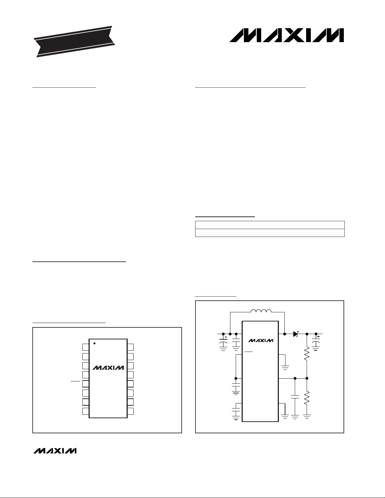
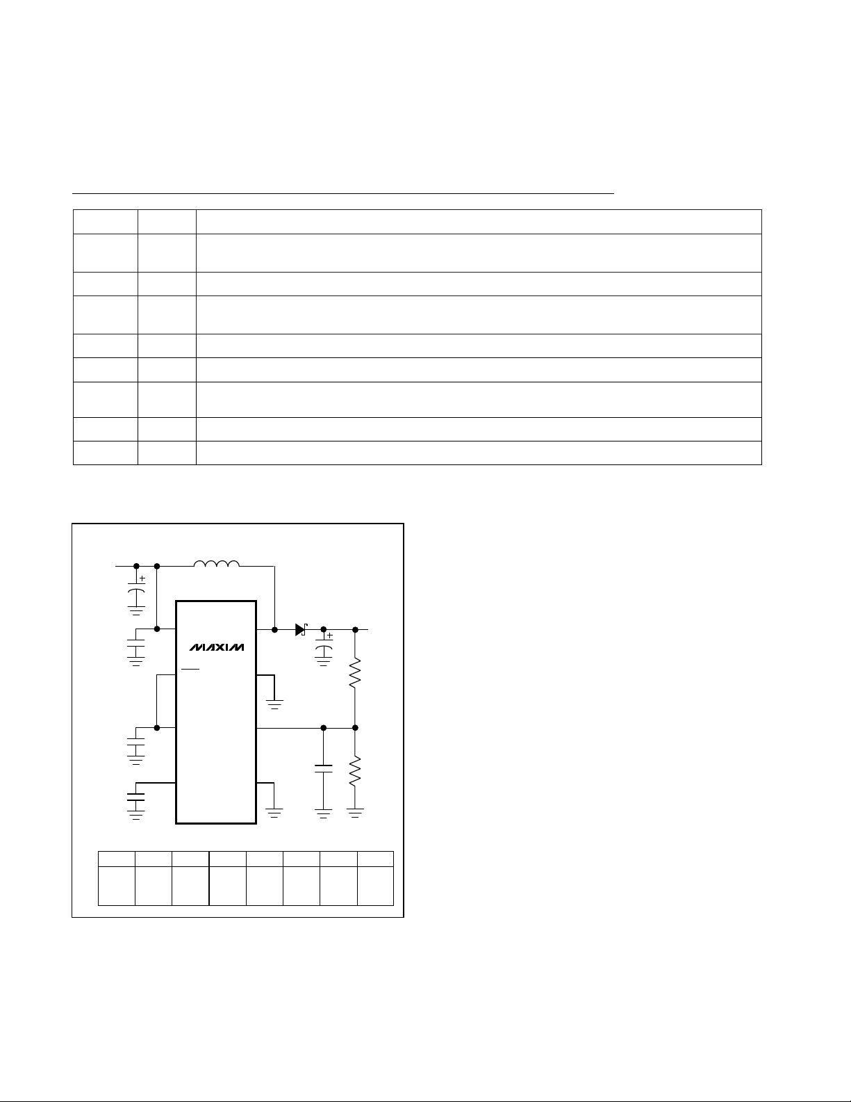
Typical Operating Circuit
19-1462; Rev 0; 6/99
EVALUATION KIT MANUAL
FOLLOWS DATA SHEET
Pin Configuration
Ordering Information
Idle Mode is a trademark of Maxim Integrated Products.
16 QSOP
PIN-PACKAGETEMP. RANGE
-40°C to +85°CMAX618EEE
PART
3V TO 28V
V
IN
IN
MAX618
SHDN
VL
COMP
LX
PGND
FB
GND
V
OUT
UP TO 28V
MAX618
28V, PWM, Step-Up DC-DC Converter
2 _______________________________________________________________________________________
ABSOLUTE MAXIMUM RATINGS
ELECTRICAL CHARACTERISTICS
(V
IN
= +6V, PGND = GND, CVL= 4.7µF, TA= 0°C to +85°C, unless otherwise noted. Typical values are at TA= +25°C.)
Stresses beyond those listed under “Absolute Maximum Ratings” may cause permanent damage to the device. These are stress ratings only, and functional
operation of the device at these or any other conditions beyond those indicated in the operational sections of the specifications is not implied. Exposure to
absolute maximum rating conditions for extended periods may affect device reliability.
IN to GND...............................................................-0.3V to +30V
LX to GND ..............................................................-0.3V to +30V
VL to GND ................................................................-0.3V to +6V
SHDN, COMP, FB to GND............................-0.3V to (VL + 0.3V)
PGND to GND.....................................................................±0.3V
Continuous Power Dissipation (T
A
= +70°C) (Note 1)
16-Pin QSOP (derate 15mW/°C above +70°C)...................1W
Operating Temperature Range ...........................-40°C to +85°C
Junction Temperature......................................................+150°C
Storage Temperature Range.............................-65°C to +150°C
Lead Temperature (soldering, 10sec).............................+300°C
Note 1: With part mounted on 0.9 in.
2
of copper.
Shutdown Supply Current I
IN
38
µA
VIN= 28V, VFB= 1.6V, SHDN = GND
Maximum Duty Cycle DC 90 95 %
PARAMETER SYMBOL MIN TYP MAX UNITS
VL Output Voltage V
VL
2.9 3.05 3.2
V
Supply Current, Full Load I
IN
2.5 3.5
mA
Supply Current, Full Load, VL
Connected to IN
I
IN
5 6.5
mA
VL Load Regulation ∆V
VL
25 40
mV
VL Undervoltage Lockout
2.58 2.7 2.8
V
FB Set Voltage V
FB
1.47 1.5 1.53
V
FB Input Bias Current I
FB
150
nA
Supply Current, No Load
Input Voltage V
IN
328
V
I
IN
500 700
µA
Line Regulation ∆V
OUT
0.01 0.08
%/V
Load Regulation ∆V
OUT
0.2
%
LX Voltage V
LX
28 V
LX Switch Current Limit I
LXON
1.7 2.2 2.7
A
Idle Mode Current-Limit
Threshold
0.25 0.35 0.45
A
LX On-Resistance R
LXON
0.3 0.6
Ω
LX Leakage Current I
LXOFF
0.02 10 µA
COMP Maximum Output Current I
COMP
100 200 µA
COMP Current vs. FB Voltage
Transconductance
0.8 1 mmho
SHDN Input Logic Low
V
IL
0.8 V
SHDN Input Logic High
V
IH
2.0 V
Shutdown Input Current 1 µA
Switching Frequency f 200 250 300 kHz
CONDITIONS
VIN= 3V to 6V, V
OUT
= 12V
VIN= 3.5V or 28V, no load
V
OUT
= 12V, I
LOAD
= 10mA to 500mA
VIN= 3.4V to 28V, VFB= 1.4V, SHDN = VL,
V
VL
< V
IN
V
IN
= 3V to 5.5V, VFB= 1.4V, SHDN = VL = IN
I
LOAD
= 0 to 2mA, VFB= 1.6V
Rising edge, 1% hysteresis
PWM mode
VFB= 1.6V
VLX= 28V
FB = GND
VIN= 3V to 28V, VFB= 1.6V, SHDN = VL
∆FB = 0.1V
SHDN = GND or VL
MAX618
28V, PWM, Step-Up DC-DC Converter
_______________________________________________________________________________________ 3
ELECTRICAL CHARACTERISTICS
(VIN= +6V, PGND = GND, CVL= 4.7µF, TA= -40°C to +85°C, unless otherwise noted.) (Note 2)
100
0
0.1 1 10 100 1000
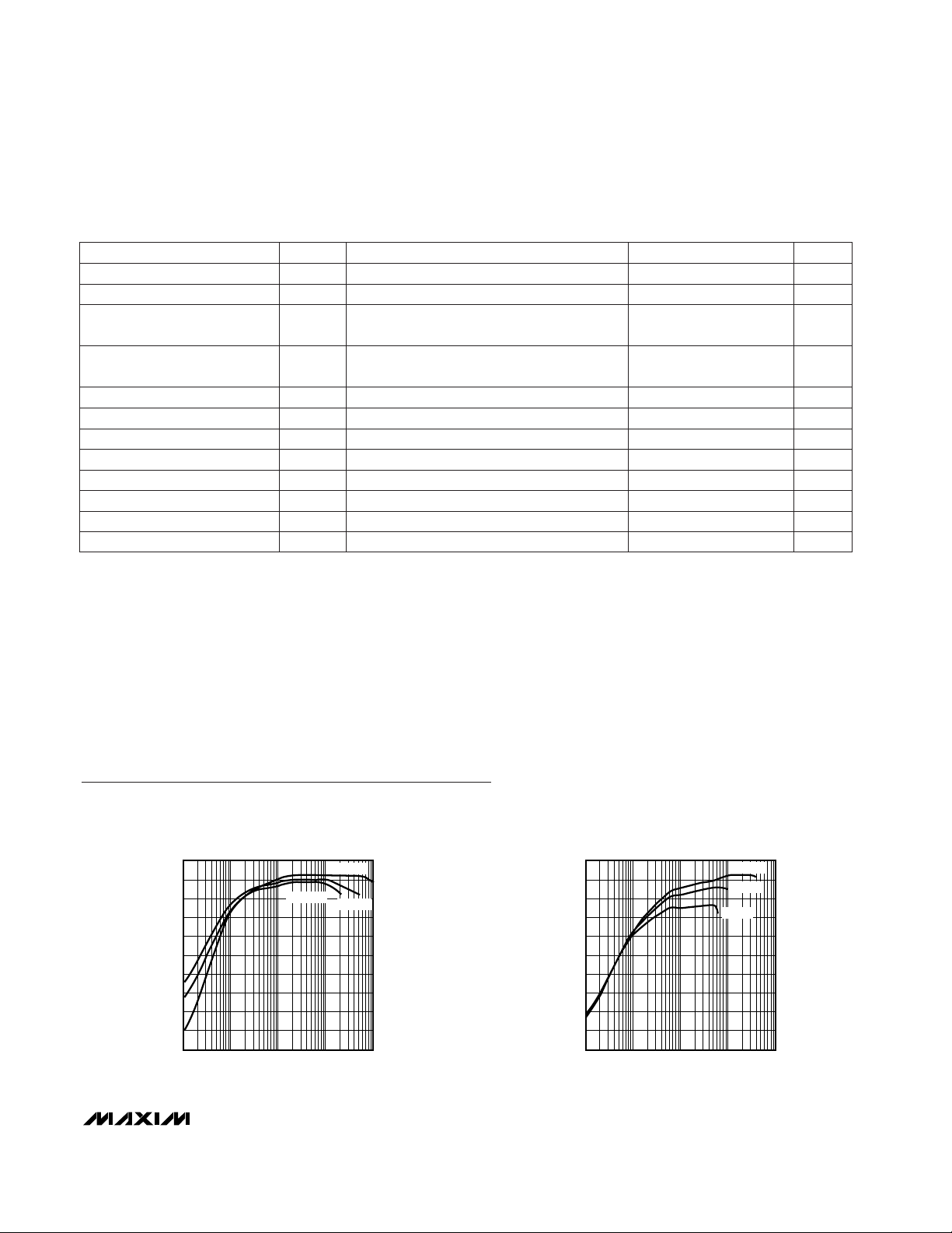
EFFICIENCY vs. OUTPUT CURRENT
(V
OUT
= 12V)
20
30
10
MAX618 toc01
OUTPUT CURRENT (mA)
EFFICIENCY (%)
40
50
60
70
80
90
VIN = 8V
VIN = 5V
VIN = 3V
100
0
0.1 1 10 100 1000
EFFICIENCY vs. OUTPUT CURRENT
(V
OUT
= 28V)
20
30
10
MAX618 toc02
OUTPUT CURRENT (mA)
EFFICIENCY (%)
40
50
60
70
80
90
VIN = 12V
VIN = 5V
VIN = 3V
Typical Operating Characteristics
(Circuit of Figure 1, TA= +25°C.)
Note 2: Specifications to -40°C are guaranteed by design, not production tested.
PARAMETER SYMBOL MIN TYP MAX UNITS
Supply Current, Full Load I
IN
4
mA
Supply Current, Full Load,
VL Connected to IN
I
IN
7.5
mA
Supply Current Shutdown I
IN
10
µA
VL Output Voltage V
VL
2.85 3.3
V
Supply Current, No Load
Input Voltage V
IN
328
V
I
IN
800
µA
VL Undervoltage Lockout V
VL
2.55 2.85
V
FB Set Voltage V
FB
1.455 1.545
V
LX Voltage Range V
LXON
28
V
LX Switch Current Limit I
LXON
1.4 3
A
LX On-Resistance R
LXON
0.6
Ω
Switching Frequency f
188 312
kHz
CONDITIONS
Rising edge, 1% hysteresis
VIN= 3.4V to 28V, VFB= 1.4V, SHDN = VL,
VL < V
IN
VIN= 3V to 5.5, VFB= 1.4V, SHDN = VL = IN
VIN= 28V, VFB= 1.6V, SHDN = GND
PWM mode
VIN= 3.5V or 28V, no load
VIN= 3V to 28V, VFB= 1.6V, SHDN = VL
MAX618
28V, PWM, Step-Up DC-DC Converter
4 _______________________________________________________________________________________
0
V
OUT
(100mV/div)
V
LX
(10V/div)
I
L
(1A/div)
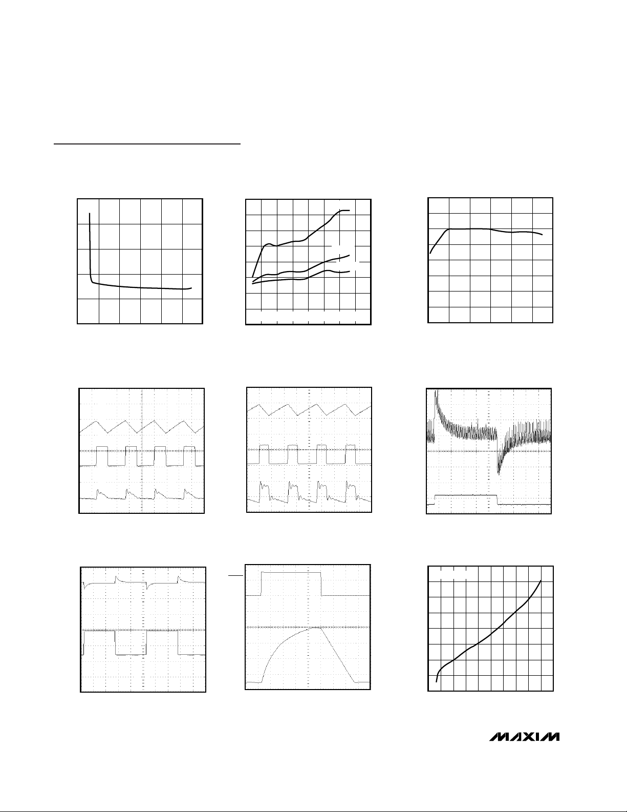
MEDIUM-LOAD SWITCHING
WAVEFORMS
MAX618 toc07
VIN = 5V, V
OUT
= 12V, I
OUT
= 200mA
2µs/div
0
V
OUT
(100mV/
div)
V
LX
(10V/div)
I
L
(1A/div)
HEAVY-LOAD SWITCHING
WAVEFORMS
MAX618 toc08
VIN = 5V, V
OUT
= 12V, I
OUT
= 500mA
2µs/div
3V
6V
V
OUT
(50mV/div)
V
IN
(5V/div)
LINE-TRANSIENT RESPONSE
MAX618 toc09
I
= 200mA, V
= 12V
2ms/div
Typical Operating Characteristics (continued)
(Circuit of Figure 1, TA= +25°C.)
0
V
OUT
(200mV/div)
I
OUT
(100mA/div)
LOAD-TRANSIENT RESPONSE
MAX618 toc10
VIN = 5V, V
OUT
= 12V
5ms/div
5V
12V
0
SHDN
(2V/div)
V
OUT
(2V/div)
SHUTDOWN RESPONSE
MAX618 toc11
VIN = 5V, V
OUT
= 12V, I
LOAD
= 500mA
500µs/div
0
0.4
0.2
0.6
1.2
1.4
1.0
0.8
1.6
2 45673 8 9 101112
MAXIMUM OUTPUT CURRENT
vs. INPUT VOLTAGE
MAX618 toc12
INPUT VOLTAGE (V)
MAXIMUM OUTPUT CURRENT (A)
V
OUT
= 12V
0.40
0.45
0.55
0.50
0.60
0.65
0105 15202530
NO-LOAD SUPPLY CURRENT
vs. INPUT VOLTAGE
MAX618 toc04
INPUT VOLTAGE (V)
SUPPLY CIRRENT (mA)
300
400
350
500
450
550
600
650
700
-50 -10 10-30 30 50 70 90 110
SUPPLY CURRENT vs. TEMPERATURE
MAX618 toc05
TEMPERATURE (°C)
SUPPLY CURRENT (µA)
VIN = 8V
VIN = 5V
VIN = 3V
INCLUDES CAPACITOR LEAKAGE CURRENT
0
0.5
1.0
1.5
2.0
2.5
3.0
3.5
4.0
2127 17222732
SHUTDOWN CURRENT
vs. SUPPLY VOLTAGE
MAX618 toc06
SUPPLY VOLTAGE (V)
SHUTDOWN CURRENT (µA)
_______________ Detailed Description
The MAX618 pulse-width modulation (PWM) DC-DC
converter with an internal 28V switch operates in a wide
range of DC-DC conversion applications including
boost, SEPIC, and flyback configurations. The MAX618
uses fixed-frequency PWM operation and Maxim’s proprietary Idle Mode control to optimize efficiency over a
wide range of loads. It also features a shutdown mode
to minimize quiescent current when not in operation.
PWM Control Scheme and
Idle Mode Operation
The MAX618 combines continuous-conduction PWM
operation at medium to high loads and Idle Mode operation at light loads to provide high efficiency over a
wide range of load conditions. The MAX618 control
scheme actively monitors the output current and automatically switches between PWM and Idle Mode to
optimize efficiency and load regulation. Figure 2 shows
a functional diagram of the MAX618’s control scheme.
The MAX618 normally operates in low-noise, continuous-conduction PWM mode, switching at 250kHz. In
PWM mode, the internal MOSFET switch turns on with
each clock pulse. It remains on until either the error
comparator trips or the inductor current reaches the 2A
switch-current limit. The error comparator compares the
feedback-error signal, current-sense signal, and slopecompensation signal in one circuit block. When the
switch turns off, energy transfers from the inductor to
MAX618
28V, PWM, Step-Up DC-DC Converter
_______________________________________________________________________________________________________ 5
Pin Description
PGND
ECB1Q503L
LX
FB
1µF
4.7µF
V
L
C
OUT
C
P
R1
R2
C
IND
V
OUT
IN
L
SHDN
GND
COMP
UP TO 28V
3V TO 28V
V
IN
C
COMP
MAX618
V
OUT
R1 R2 C
IND
LC
OUT
CPC
COMP
8V 402kΩ 93.1kΩ 150µF12µH 150µF 220pF 0.082µF
12V 715kΩ 100kΩ 100µF15µH 100µH 56pF 0.1µF
28V 574kΩ 32.4kΩ 86µF39µH33µF 47pF 0.47µF
Figure 1. Single-Supply Operation
Feedback Input. Connect a resistor-divider network to set V
OUT
. FB threshold is 1.5V.FB7
LDO Regulator Supply Input. IN accepts inputs up to +28V. Bypass to GND with a 1µF ceramic capacitor
as close to pins 10 and 12 as possible.
IN10
Internal 3.1V LDO Regulator Output. Bypass to GND with a 4.7µF capacitor.VL11
Power Ground, source of internal N-channel switchPGND13, 14, 15
Compensation Input. Bypass to GND with the capacitance value shown in Table 2.COMP6
Shutdown Input. A logic low puts the MAX618 in shutdown mode and reduces supply current to 3µA.
SHDN must not exceed VL. In shutdown, the output falls to VINless one diode drop.
SHDN
5
PIN
Drain of internal N-channel switch. Connect the inductor between IN and LX.LX2, 3, 4
GroundGND
1, 8, 9,
12, 16
FUNCTIONNAME
 Loading...