

Page 1
For free samples & the latest literature: http://www.maxim-ic.com, or phone 1-800-998-8800.
For small orders, phone 1-800-835-8769.
General Description
The MAX618 CMOS, PWM, step-up DC-DC converter
generates output voltages up to 28V and accepts
inputs from +3V to +28V. An internal 2A, 0.3Ω switch
eliminates the need for external power MOSFETs while
supplying output currents up to 500mA or more. A
PWM control scheme combined with Idle Mode™ operation at light loads minimizes noise and ripple while
maximizing efficiency over a wide load range. No-load
operating current is 500µA, which allows efficiency up
to 93%.
A fast 250kHz switching frequency allows the use of
small surface-mount inductors and capacitors. A shutdown mode extends battery life when the device is not
in use. Adaptive slope compensation allows the
MAX618 to accommodate a wide range of input and
output voltages with a simple, single compensation
capacitor.
The MAX618 is available in a thermally enhanced 16pin QSOP package that is the same size as an industrystandard 8-pin SO but dissipates up to 1W. An
evaluation kit (MAX618EVKIT) is available to help
speed designs.
Applications
Automotive-Powered DC-DC Converters
Industrial +24V and +28V Systems
LCD Displays
Palmtop Computers
Features
♦ Adjustable Output Voltage Up to +28V
♦ Up to 93% Efficiency
♦ Wide Input Voltage Range (+3V to +28V)
♦ Up to 500mA Output Current at +12V
♦ 500µA Quiescent Supply Current
♦ 3µA Shutdown Current
♦ 250kHz Switching Frequency
♦ Small 1W 16-Pin QSOP Package
MAX618
28V, PWM, Step-Up DC-DC Converter
________________________________________________________________ Maxim Integrated Products 1
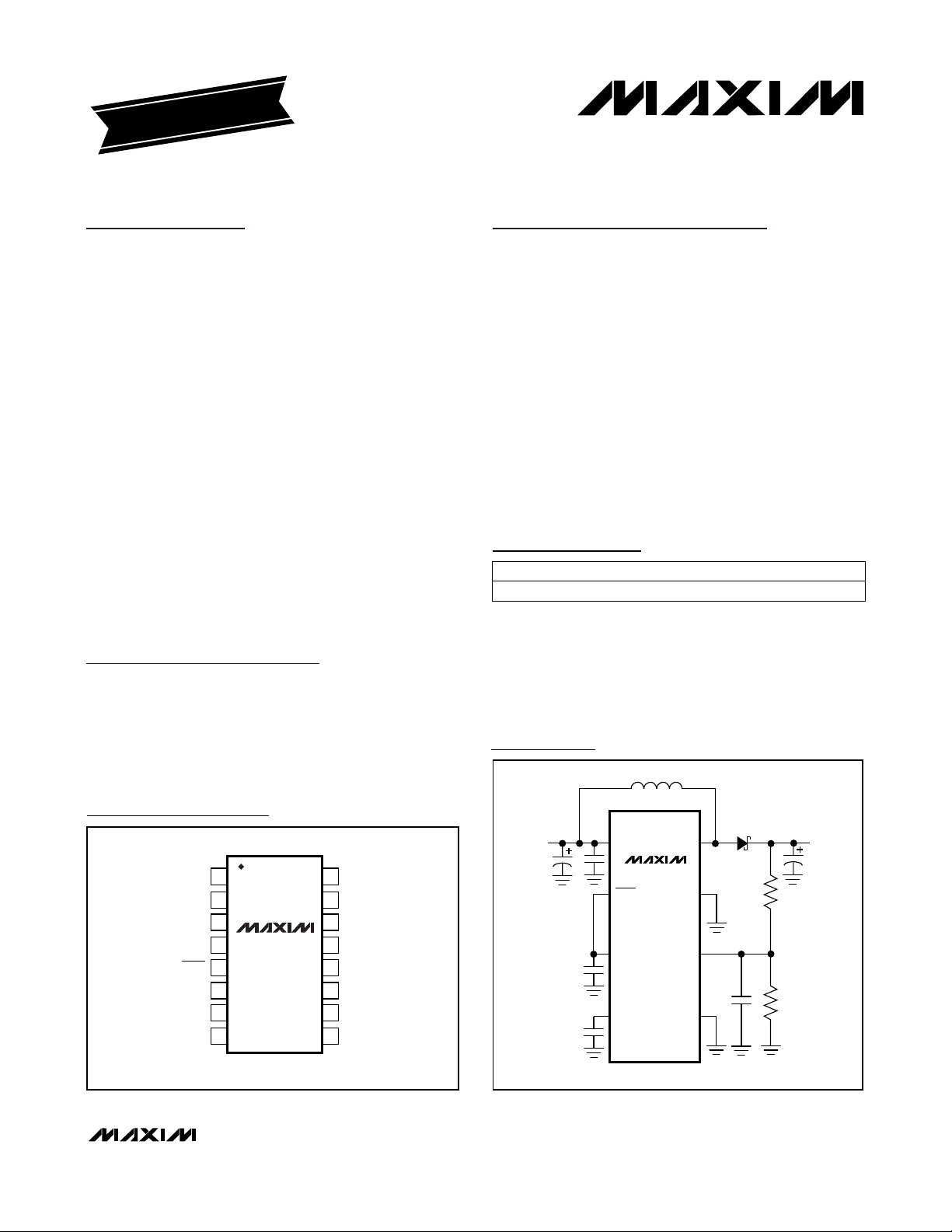
Typical Operating Circuit
19-1462; Rev 0; 6/99
Pin Configuration
Ordering Information
Idle Mode is a trademark of Maxim Integrated Products.
16 QSOP
PIN-PACKAGETEMP. RANGE
-40°C to +85°CMAX618EEE
PART
EVALUATION KIT
AVAILABLE
V
TOP VIEW
16
15
PGND
14
PGND
13
PGND
12
GND
VL
11
10
IN
9
GND
1
GND GND
LX
2
LX
3
MAX618
4
LX
SHDN
5
COMP
6
FB
7
GND
8
QSOP
3V TO 28V
IN
IN
MAX618
SHDN
VL
COMP
LX
PGND
FB
GND
V
OUT
UP TO 28V
Page 2
MAX618
28V, PWM, Step-Up DC-DC Converter
2 _______________________________________________________________________________________
ABSOLUTE MAXIMUM RATINGS
ELECTRICAL CHARACTERISTICS
(V
IN
= +6V, PGND = GND, CVL= 4.7µF, TA= 0°C to +85°C, unless otherwise noted. Typical values are at TA= +25°C.)
Stresses beyond those listed under “Absolute Maximum Ratings” may cause permanent damage to the device. These are stress ratings only, and functional
operation of the device at these or any other conditions beyond those indicated in the operational sections of the specifications is not implied. Exposure to
absolute maximum rating conditions for extended periods may affect device reliability.
IN to GND ...............................................................-0.3V to +30V
LX to GND ..............................................................-0.3V to +30V
VL to GND ................................................................-0.3V to +6V
SHDN, COMP, FB to GND ............................-0.3V to (VL + 0.3V)
PGND to GND.....................................................................±0.3V
Continuous Power Dissipation (T
A
= +70°C) (Note 1)
16-Pin QSOP (derate 15mW/°C above +70°C)...................1W
Operating Temperature Range ...........................-40°C to +85°C
Junction Temperature......................................................+150°C
Storage Temperature Range .............................-65°C to +150°C
Lead Temperature (soldering, 10sec) .............................+300°C
Note 1: With part mounted on 0.9 in.
2
of copper.
Shutdown Supply Current I
IN
38
µA
VIN= 28V, VFB= 1.6V, SHDN = GND
Maximum Duty Cycle DC 90 95 %
PARAMETER SYMBOL MIN TYP MAX UNITS
VL Output Voltage V
VL
2.9 3.05 3.2
V
Supply Current, Full Load I
IN
2.5 3.5
mA
Supply Current, Full Load, VL
Connected to IN
I
IN
5 6.5
mA
VL Load Regulation ∆V
VL
25 40
mV
VL Undervoltage Lockout
2.58 2.7 2.8
V
FB Set Voltage V
FB
1.47 1.5 1.53
V
FB Input Bias Current I
FB
150
nA
Supply Current, No Load
Input Voltage V
IN
328
V
I
IN
500 700
µA
Line Regulation ∆V
OUT
0.01 0.08
%/V
Load Regulation ∆V
OUT
0.2
%
LX Voltage V
LX
28 V
LX Switch Current Limit I
LXON
1.7 2.2 2.7
A
Idle Mode Current-Limit
Threshold
0.25 0.35 0.45
A
LX On-Resistance R
LXON
0.3 0.6 Ω
LX Leakage Current I
LXOFF
0.02 10 µA
COMP Maximum Output Current I
COMP
100 200 µA
COMP Current vs. FB Voltage
Transconductance
0.8 1 mmho
SHDN Input Logic Low
V
IL
0.8 V
SHDN Input Logic High
V
IH
2.0 V
Shutdown Input Current 1 µA
Switching Frequency f 200 250 300 kHz
CONDITIONS
VIN= 3V to 6V, V
OUT
= 12V
VIN= 3.5V or 28V, no load
V
OUT
= 12V, I
LOAD
= 10mA to 500mA
VIN= 3.4V to 28V, VFB= 1.4V, SHDN = VL,
V
VL
< V
IN
V
IN
= 3V to 5.5V, VFB= 1.4V, SHDN = VL = IN
I
LOAD
= 0 to 2mA, VFB= 1.6V
Rising edge, 1% hysteresis
PWM mode
VFB= 1.6V
VLX= 28V
FB = GND
VIN= 3V to 28V, VFB= 1.6V, SHDN = VL
∆FB = 0.1V
SHDN = GND or VL
Page 3
MAX618
28V, PWM, Step-Up DC-DC Converter
_______________________________________________________________________________________ 3
ELECTRICAL CHARACTERISTICS
(VIN= +6V, PGND = GND, CVL= 4.7µF, TA= -40°C to +85°C, unless otherwise noted.) (Note 2)
100
0
0.1 1 10 100 1000
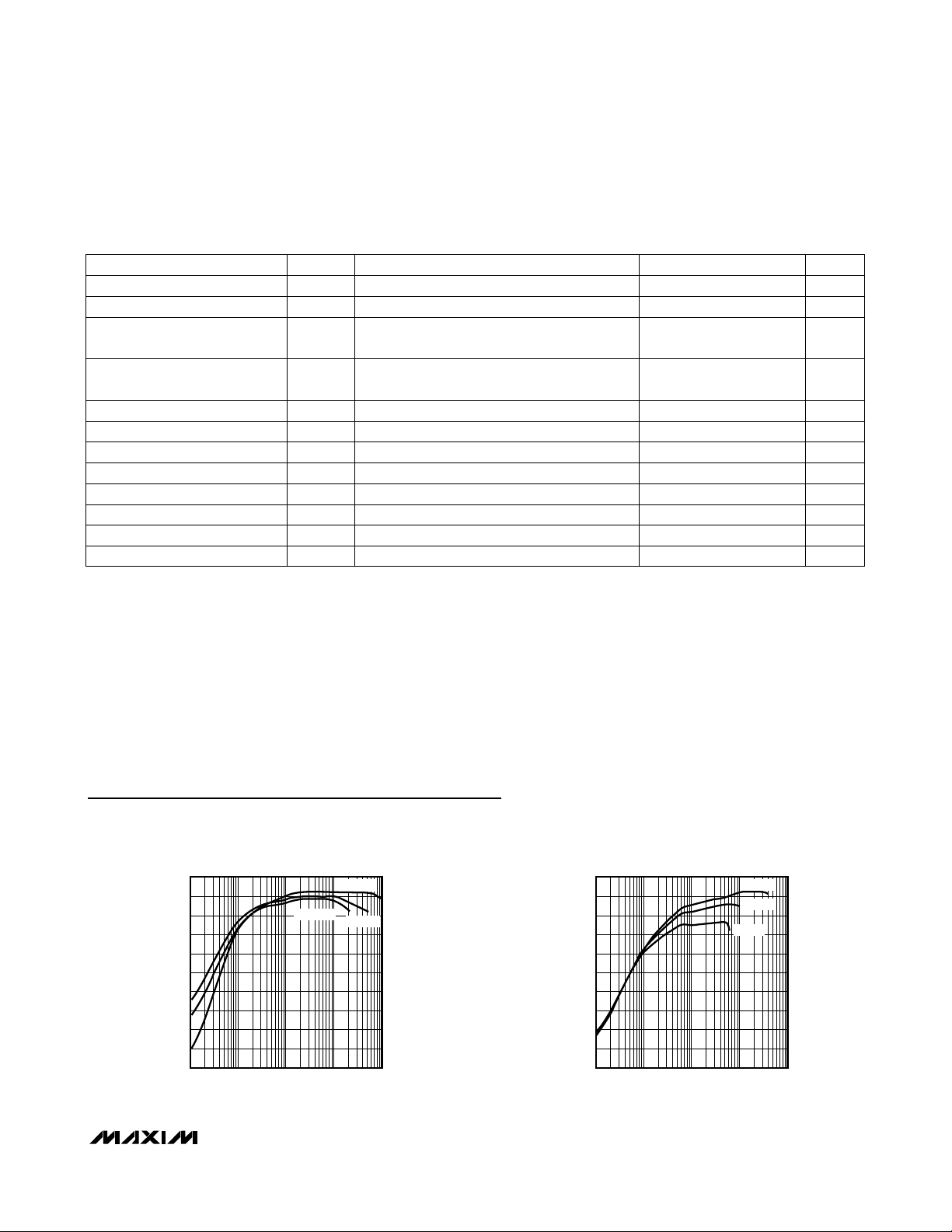
EFFICIENCY vs. OUTPUT CURRENT
(V
OUT
= 12V)
20
30
10
MAX618 toc01
OUTPUT CURRENT (mA)
EFFICIENCY (%)
40
50
60
70
80
90
VIN = 8V
VIN = 5V
VIN = 3V
100
0
0.1 1 10 100 1000
EFFICIENCY vs. OUTPUT CURRENT
(V
OUT
= 28V)
20
30
10
MAX618 toc02
OUTPUT CURRENT (mA)
EFFICIENCY (%)
40
50
60
70
80
90
VIN = 12V
VIN = 5V
VIN = 3V
Typical Operating Characteristics
(Circuit of Figure 1, TA= +25°C.)
Note 2: Specifications to -40°C are guaranteed by design, not production tested.
PARAMETER SYMBOL MIN TYP MAX UNITS
Supply Current, Full Load I
IN
4
mA
Supply Current, Full Load,
VL Connected to IN
I
IN
7.5
mA
Supply Current Shutdown I
IN
10
µA
VL Output Voltage V
VL
2.85 3.3
V
Supply Current, No Load
Input Voltage V
IN
328
V
I
IN
800
µA
VL Undervoltage Lockout V
VL
2.55 2.85
V
FB Set Voltage V
FB
1.455 1.545
V
LX Voltage Range V
LXON
28
V
LX Switch Current Limit I
LXON
1.4 3
A
LX On-Resistance R
LXON
0.6
Ω
Switching Frequency f
188 312
kHz
CONDITIONS
Rising edge, 1% hysteresis
VIN= 3.4V to 28V, VFB= 1.4V, SHDN = VL,
VL < V
IN
VIN= 3V to 5.5, VFB= 1.4V, SHDN = VL = IN
VIN= 28V, VFB= 1.6V, SHDN = GND
PWM mode
VIN= 3.5V or 28V, no load
VIN= 3V to 28V, VFB= 1.6V, SHDN = VL
Page 4
MAX618
28V, PWM, Step-Up DC-DC Converter
4 _______________________________________________________________________________________
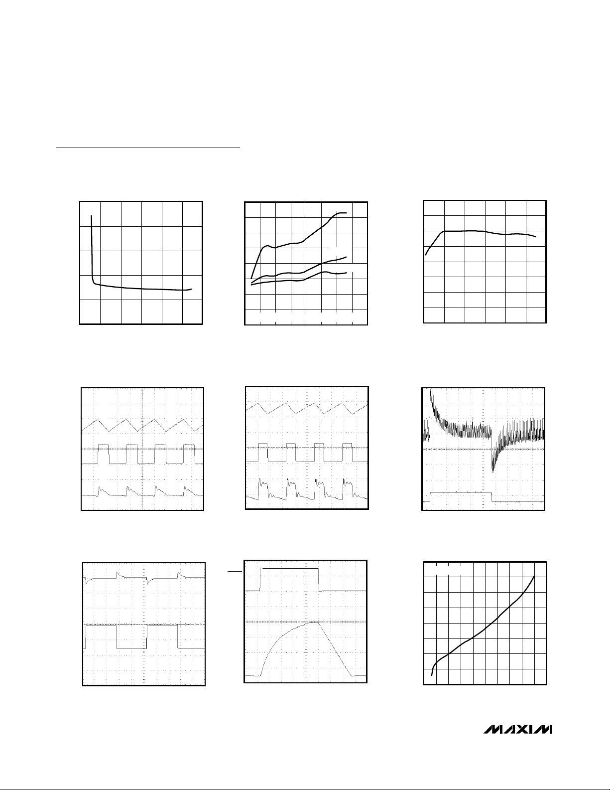
Typical Operating Characteristics (continued)
(Circuit of Figure 1, TA= +25°C.)
0
V
OUT
(200mV/div)
I
OUT
(100mA/div)
LOAD-TRANSIENT RESPONSE
MAX618 toc10
VIN = 5V, V
OUT
= 12V
5ms/div
5V
12V
0
SHDN
(2V/div)
V
OUT
(2V/div)
SHUTDOWN RESPONSE
MAX618 toc11
VIN = 5V, V
OUT
= 12V, I
LOAD
= 500mA
500µs/div
0
0.4
0.2
0.6
1.2
1.4
1.0
0.8
1.6
2 45673 8 9 101112
MAXIMUM OUTPUT CURRENT
vs. INPUT VOLTAGE
MAX618 toc12
INPUT VOLTAGE (V)
MAXIMUM OUTPUT CURRENT (A)
V
OUT
= 12V
0.40
0.45
0.55
0.50
0.60
0.65
0105 15202530
NO-LOAD SUPPLY CURRENT
vs. INPUT VOLTAGE
MAX618 toc04
INPUT VOLTAGE (V)
SUPPLY CIRRENT (mA)
300
400
350
500
450
550
600
650
700
-50 -10 10-30 30507090110
SUPPLY CURRENT vs. TEMPERATURE
MAX618 toc05
TEMPERATURE (°C)
SUPPLY CURRENT (µA)
VIN = 8V
VIN = 5V
VIN = 3V
INCLUDES CAPACITOR LEAKAGE CURRENT
0
0.5
1.0
1.5
2.0
2.5
3.0
3.5
4.0
2127 17222732
SHUTDOWN CURRENT
vs. SUPPLY VOLTAGE
MAX618 toc06
SUPPLY VOLTAGE (V)
SHUTDOWN CURRENT (µA)
MEDIUM-LOAD SWITCHING
I
L
(1A/div)
V
LX
(10V/div)
V
OUT
(100mV/div)
VIN = 5V, V
OUT
WAVEFORMS
2µs/div
= 12V, I
OUT
= 200mA
MAX618 toc07
HEAVY-LOAD SWITCHING
WAVEFORMS
I
L
(1A/div)
0
V
LX
(10V/div)
V
OUT
(100mV/
div)
2µs/div
VIN = 5V, V
OUT
= 12V, I
OUT
= 500mA
MAX618 toc08
V
(50mV/div)
0
(5V/div)
LINE-TRANSIENT RESPONSE
OUT
V
IN
I
= 200mA, V
MAX618 toc09
6V
3V
2ms/div
= 12V
Page 5
_______________ Detailed Description
The MAX618 pulse-width modulation (PWM) DC-DC
converter with an internal 28V switch operates in a wide
range of DC-DC conversion applications including
boost, SEPIC, and flyback configurations. The MAX618
uses fixed-frequency PWM operation and Maxim’s proprietary Idle Mode control to optimize efficiency over a
wide range of loads. It also features a shutdown mode
to minimize quiescent current when not in operation.
PWM Control Scheme and
Idle Mode Operation
The MAX618 combines continuous-conduction PWM
operation at medium to high loads and Idle Mode operation at light loads to provide high efficiency over a
wide range of load conditions. The MAX618 control
scheme actively monitors the output current and automatically switches between PWM and Idle Mode to
optimize efficiency and load regulation. Figure 2 shows
a functional diagram of the MAX618’s control scheme.
The MAX618 normally operates in low-noise, continuous-conduction PWM mode, switching at 250kHz. In
PWM mode, the internal MOSFET switch turns on with
each clock pulse. It remains on until either the error
comparator trips or the inductor current reaches the 2A
switch-current limit. The error comparator compares the
feedback-error signal, current-sense signal, and slopecompensation signal in one circuit block. When the
switch turns off, energy transfers from the inductor to
MAX618
28V, PWM, Step-Up DC-DC Converter
_______________________________________________________________________________________________________ 5
Pin Description
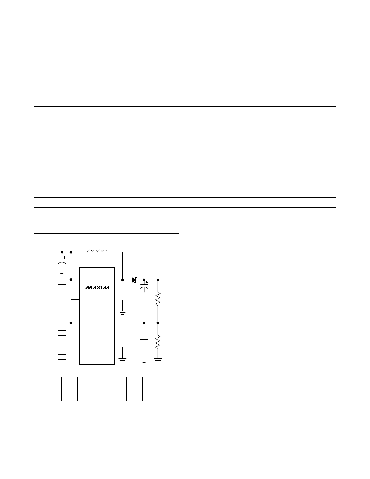
Figure 1. Single-Supply Operation
Feedback Input. Connect a resistor-divider network to set V
OUT
. FB threshold is 1.5V.FB7
LDO Regulator Supply Input. IN accepts inputs up to +28V. Bypass to GND with a 1µF ceramic capacitor
as close to pins 10 and 12 as possible.
IN10
Internal 3.1V LDO Regulator Output. Bypass to GND with a 4.7µF capacitor.VL11
Power Ground, source of internal N-channel switchPGND13, 14, 15
Compensation Input. Bypass to GND with the capacitance value shown in Table 2.COMP6
Shutdown Input. A logic low puts the MAX618 in shutdown mode and reduces supply current to 3µA.
SHDN must not exceed VL. In shutdown, the output falls to V
IN
less one diode drop.
SHDN
5
PIN
Drain of internal N-channel switch. Connect the inductor between IN and LX.LX2, 3, 4
GroundGND
1, 8, 9,
12, 16
FUNCTIONNAME
IN
SHDN
V
L
COMP
L
MAX618
PGND
IND
3V TO 28V
V
IN
C
IND
1µF
4.7µF
C
COMP
V
R1 R2 C
OUT
8V 402kΩ 93.1kΩ 150µF12µH 150µF 220pF 0.082µF
12V 715kΩ 100kΩ 100µF15µH 100µH 56pF 0.1µF
28V 574kΩ 32.4kΩ 86µF39µH33µF 47pF 0.47µF
LX
FB
GND
LC
ECB1Q503L
C
P
OUT
C
OUT
CPC
V
OUT
UP TO 28V
R1
R2
COMP
Page 6

MAX618
the output capacitor. Output current is limited by the 2A
MOSFET current limit and the MAX618’s package
power-dissipation limit. See the Maximum Output
Current section for details.
In Idle Mode, the MAX618 improves light-load efficiency by reducing inductor current and skipping cycles to
reduce the losses in the internal switch, diode, and
inductor. In this mode, a switching cycle initiates only
when the error comparator senses that the output voltage is about to drop out of regulation. When this
occurs, the NMOS switch turns on and remains on until
the inductor current exceeds the nominal 350mA Idle
Mode current limit.
Refer to Table 1 for an estimate of load currents at which
the MAX618 transitions between PWM and Idle Mode.
Compensation Scheme
Although the higher loop gain of voltage-controlled
architectures tends to provide tighter load regulation,
current-controlled architectures are generally easier to
compensate over wide input and output voltage
ranges. The MAX618 uses both control schemes in parallel: the dominant, low-frequency components of the
error signal are tightly regulated with a voltage-control
loop, while a current-control loop improves stability at
higher frequencies. Compensation is achieved through
the selection of the output capacitor (C
OUT
), the inte-
grator capacitor (C
COMP
), and the pole capacitor (CP)
from FB to GND. CPcancels the zero formed by C
OUT
and its ESR. Refer to the Capacitor Selection section for
guidance on selecting these capacitors.
VL Low-Dropout Regulator
The MAX618 contains a 3.1V low-dropout linear regulator to power internal circuitry. The regulator’s input is IN
and its output is VL. The IN to VL dropout voltage is
100mV, so that when IN is less than 3.2V, VL is typically
100mV below IN. The MAX618 still operates when the
LDO is in dropout, as long as VL remains above the
2.7V undervoltage lockout. Bypass VL with a 4.7µF
ceramic capacitor placed as close to the VL and GND
pins as possible.
28V, PWM, Step-Up DC-DC Converter
6 _______________________________________________________________________________________
Figure 2. Functional Diagram
IDLE MODE
CURRENT LIMIT
GND
SHDN
SHUTDOWN
ERROR
COMPARATOR
SLOPE
COMPENSATION
THERMAL
SHUTDOWN
CURRENT LIMIT
250kHz
OSCILLATOR
REFERENCE
PWM
PWM
LOGIC
MAX618
CURRENT-
SENSE
CIRCUIT
VL
NMOS
R
14R
INTEGRATOR
LINEAR
REGULATOR
IN
PGND
LX OUT
FB
COMP
IN
VL
Page 7

MAX618
28V, PWM, Step-Up DC-DC Converter
_______________________________________________________________________________________ 7
Table 1. PWM/Idle-Mode Transition Load Current (I
OUT
in Amps) vs. Input and Output Voltage
OUT
V
45678910111213141516171819202122232425262728
IN
3 0.20 0.20 0.18 0.15 0.12 0.10 0.09 0.08 0.07 0.06 0.05 0.04 0.04 0.04 0.03 0.03 0.03 0.03 0.03 0.02 0.02 0.02 0.02 0.02 0.02
4 0.18 0.21 0.20 0.17 0.15 0.13 0.12 0.10 0.09 0.08 0.07 0.07 0.06 0.05 0.05 0.04 0.04 0.04 0.03 0.03 0.03 0.03 0.03 0.03
5 0.16 0.20 0.21 0.19 0.17 0.16 0.14 0.13 0.11 0.10 0.09 0.09 0.08 0.07 0.07 0.06 0.06 0.05 0.05 0.04 0.04 0.04 0.04
6 0.15 0.20 0.21 0.20 0.19 0.18 0.16 0.15 0.13 0.12 0.11 0.10 0.10 0.09 0.08 0.08 0.07 0.07 0.06 0.06 0.05 0.05
7 0.17 0.19 0.21 0.21 0.20 0.19 0.17 0.16 0.15 0.14 0.13 0.12 0.11 0.10 0.10 0.09 0.08 0.08 0.07 0.07 0.07
8 0.19 0.18 0.20 0.21 0.20 0.20 0.19 0.17 0.16 0.15 0.14 0.13 0.13 0.12 0.11 0.10 0.10 0.09 0.09 0.08
9 0.20 0.17 0.20 0.21 0.21 0.20 0.19 0.18 0.18 0.17 0.16 0.15 0.14 0.13 0.12 0.12 0.11 0.10 0.10
10 0.21 0.16 0.19 0.20 0.21 0.21 0.20 0.19 0.18 0.17 0.17 0.16 0.15 0.14 0.13 0.13 0.12 0.11
11 0.22 0.15 0.19 0.20 0.21 0.21 0.20 0.20 0.19 0.18 0.17 0.17 0.16 0.15 0.14 0.14 0.13
12 0.23 0.15 0.18 0.20 0.21 0.21 0.21 0.20 0.20 0.19 0.18 0.18 0.17 0.16 0.15 0.15
13 0.24 0.16 0.17 0.19 0.20 0.21 0.21 0.20 0.20 0.19 0.19 0.18 0.17 0.17 0.16
14 0.25 0.17 0.17 0.19 0.20 0.21 0.21 0.21 0.20 0.20 0.19 0.19 0.18 0.17
15 0.25 0.18 0.16 0.18 0.20 0.20 0.21 0.21 0.21 0.20 0.20 0.19 0.19
16 0.26 0.19 0.16 0.18 0.19 0.20 0.21 0.21 0.21 0.20 0.20 0.20
17 0.26 0.20 0.15 0.17 0.19 0.20 0.20 0.21 0.21 0.21 0.20
18 0.27 0.20 0.15 0.17 0.19 0.20 0.20 0.21 0.21 0.21
V
19 0.27 0.21 0.16 0.17 0.18 0.19 0.20 0.21 0.21
20 0.27 0.21 0.17 0.16 0.18 0.19 0.20 0.20
21 0.28 0.22 0.17 0.16 0.18 0.19 0.20
22 0.28 0.22 0.18 0.15 0.17 0.19
23 0.28 0.23 0.18 0.15 0.17
24 0.28 0.23 0.19 0.15
25 0.29 0.24 0.19
26 0.29 0.24
27 0.29
Page 8

MAX618
28V, PWM, Step-Up DC-DC Converter
8 _______________________________________________________________________________________
Figure 3. Dual-Supply Operation (VIN= 2.7V to 5.5V)
Figure 4. Dual-Supply Operation (V
IN
= 3V to 28V)
Table 2. Input Configurations
VL can be overdriven by an external supply between
2.7V and 5.5V. In systems with +3.3V or +5V logic
power supplies available, improve efficiency by powering VL and V
IN
directly from the logic supply as shown
in Figure 3.
Operating Configurations
The MAX618 can be connected in one of three configurations described in Table 2 and shown in Figures 1, 3, and
4. The VL linear regulator allows operation from a single
supply between +3V and +28V as shown in Figure 1.
The circuit in Figure 3 allows a logic supply to power
the MAX618 while using a separate source for DC-DC
conversion power (inductor voltage). The logic supply
(between 2.7V and 5.5V) connects to VL and IN. VL =
IN; voltages of 3.3V or more improve efficiency by providing greater gate drive for the internal MOSFET.
The circuit in Figure 4 allows separate supplies to
power IN and the inductor voltage. It differs from the
connection in Figure 3 in that the MAX618 chip supply
is not limited to 5.5V.
CIRCUIT
Figure 1
Input voltage connects
to IN and inductor.
CONNECTION
V
IN
RANGE
3V to V
OUT
(up to 28V)
V
IN
INDUCTOR
VOLTAGE
BENEFITS/COMMENTS
• Single-supply operation.
• SHDN must be connected to or pulled up to VL. On/off
control requires an open-drain or open-collector connection
to SHDN.
Figure 3
Figure 4
0 to V
OUT
(up to 28V)
0 to V
OUT
(up to 28V)
• Increased efficiency.
• SHDN can be driven by logic powered from the supply con-
nected to IN and VL, or can be connected to or pulled up to
VL.
• Input power source (inductor voltage) is separate from the
MAX618’s bias (V
IN
= VL) and can be less than or greater
than VIN.
• Input power source (inductor voltage) is separate from the
MAX618’s bias (V
IN
) and can be less than or greater than
V
IN
.
• SHDN must be connected to or pulled up to VL. On/off
control requires an open-drain or open-collector connection
to SHDN.
IN and inductor voltage supplied by separate sources.
IN and VL connect
together. Inductor voltage supplied by a
separate source.
2.7V to 5.5V
3V to 28V
V
2.7V TO 5.5V
1µF
IND
UP TO 28V
C
IN
4.7µF
C
COMP
IND
IN
SHDN
VL
COMP
L
MAX618
PGND
GND
LX
C
OUT
FB
C
P
OUT
UP TO 28V
R1
R2
V
IND
UP TO 28V
IN
3V TO 28V
4.7µF
C
COMP
C
1µF
IND
IN
SHDN
VL
COMP
L
LX
MAX618
PGND
FB
GND
C
OUT
C
P
OUT
UP TO 28V
R1
R2
Page 9

Shutdown Mode
In shutdown mode (SHDN = 0), the MAX618’s feedback and control circuit, reference, and internal biasing
circuitry turn off and reduce the IN supply current to
3µA (10µA max). When in shutdown, a current path
remains from the input to the output through the external inductor and diode. Consequently, the output falls
to V
IN
less one diode drop in shutdown.
SHDN may not exceed VL. For always-on operation,
connect SHDN to VL. To add on/off control to the circuit
of Figure 1 or 4, pull SHDN to VL with a resistor (10kΩ
to 100kΩ) and drive SHDN with an open-drain logic
gate or switch as shown in Figure 5. Alternatively, the
circuit of Figure 3 allows direct SHDN drive by any
logic-level gate powered from the same supply that
powers VL and IN, as shown in Figure 6.
__________________Design Procedure
The MAX618 operates in a number of DC-DC converter
configurations including step-up, SEPIC, and flyback.
The following design discussion is limited to step-up
converters.
Setting the Output Voltage
Two external resistors (R1 and R2) set the output voltage. First, select a value for R2 between 10kΩ and
200kΩ. Calculate R1 with:
where VFBis 1.5V.
Determining the Inductor Value
The MAX618’s high switching frequency allows the use
of a small value inductor. The recommended inductor
value is proportional to the output voltage and is given
by the following:
After solving for the above equation, round down as
necessary to select a standard inductor value.
When selecting an inductor, choose one rated to
250kHz, with a saturation current exceeding the peak
inductor current, and with a DC resistance under
200mΩ. Ferrite core or equivalent inductors are generally appropriate (see MAX618 EV kit data sheet).
Calculate the peak inductor current with the following
equation:
Note that the peak inductor current is internally limited
to 2A.
Diode Selection
The MAX618’s high switching frequency demands a
high-speed rectifier. Schottky diodes are preferred for
most applications because of their fast recovery time
and low forward voltage. Make sure that the diode’s
peak current rating exceeds the 2A peak switch current, and that its breakdown voltage exceeds the output voltage.
()
MAX618
28V, PWM, Step-Up DC-DC Converter
_______________________________________________________________________________________ 9
Figure 5. Adding On/Off Control to Circuit of Figure 1 or 4
Figure 6. Adding On/Off Control to Circuit of Figure 3
MAX618
VL
OPEN-DRAIN
LOGIC
100k
SHDN
ON/OFF
CONTROL
⎛
V
RR
12 1= −
OUT
⎜
V
⎝
FB
⎞
⎟
⎠
MAX618
IN
SYSTEM
LOGIC SUPPLY
SYSTEM LOGIC
ON/OFF
CONTROL
VL
SHDN
V
OUT
L
=
5
⋅710
I I
LX(PEAK) OUT
=+
V
OUT
V
IN
µ
2s
⎛
⎞
V
IN
⎜
⎟
⎜
L
⎜
⎠
⎝
VV
OUT IN
V
OUT
⎛
⎜
⎝
⎞
−
⎟
⎟
⎟
⎠
Page 10

MAX618
28V, PWM, Step-Up DC-DC Converter
10 ______________________________________________________________________________________
Maximum Output Current
The MAX618’s 2.2A LX current limit determines the
output power that can be supplied for most applications. In some cases, particularly when the input voltage is low, output power is sometimes restricted by
package dissipation limits. The MAX618 is protected
by a thermal shutdown circuit that turns off the switch
when the die temperature exceeds +150°C. When the
device cools by 10°C, the switch is enabled again.
Table 3 details output current with a variety of input and
output voltages. Each listing in Table 3 is either the limit
set by an LX current limit or by package dissipation at
+85°C ambient, whichever is lower. The values in Table
3 assume a 40mΩ inductor resistance.
Capacitor Selection
Input Capacitors
The input bypass capacitor, C
IND
, reduces the input
ripple created by the boost configuration. High-impedance sources require high C
IND
values. However, 68µF
is generally adequate for input currents up to 2A. Low
ESR capacitors are recommended because they will
decrease the ripple created on the input and improve
efficiency. Capacitors with ESR below 0.3Ω are generally appropriate.
In addition to the input bypass capacitor, bypass IN
with a 1µF ceramic capacitor placed as close to the IN
and GND pins as possible. Bypass VL with a 4.7µF
ceramic capacitor placed as close to the VL and GND
pins as possible.
Output Capacitor
Use Table 4 to find the minimum output capacitance
necessary to ensure stable operation. In addition,
choose an output capacitor with low ESR to reduce the
output ripple. The dominant component of output ripple
is the product of the peak-to-peak inductor ripple current and the ESR of the output capacitor. ESR below
50mΩ generates acceptable levels of output ripple for
most applications.
Integrator Capacitor
The compensation capacitor (C
COMP
) sets the dominant pole in the MAX618’s transfer function. The proper
compensation capacitance depends upon output
capacitance. Table 5 shows the capacitance value
needed for the output capacitances specified in Table
4. However, if a different output capacitor is used (e.g.,
a standard value), then recalculate the value of capacitance needed for the integrator capacitor with the following formula:
Pole Compensation Capacitor
The pole capacitor (CP) cancels the unwanted zero
introduced by C
OUT
’s ESR, and thereby ensures stability in PWM operation. The exact value of the pole
capacitor is not critical, but it should be near the value
calculated by the following equation:
where R
ESR
is C
OUT
’s ESR.
Layout Considerations
Proper PC board layout is essential due to high current
levels and fast switching waveforms that radiate noise.
Use the MAX618 evaluation kit or equivalent PC layout
to perform initial prototyping. Breadboards, wire-wrap,
and proto-boards are not recommended when prototyping switching regulators.
It is important to connect the GND pin, the input
bypass capacitor ground lead, and the output filter
capacitor ground lead to a single point to minimize
ground noise and improve regulation. Also, minimize
lead lengths to reduce stray capacitance, trace resistance, and radiated noise, with preference given to the
feedback circuit, the ground circuit, and LX. Place the
feedback resistors as close to the FB pin as possible.
Place a 1µF input bypass capacitor as close as possible to IN and GND.
Refer to the MAX618 evaluation kit for an example of
proper board layout.
C
COMP
C Table C
COMP OUT
=
C Table
OUT
⋅( )
5
( )
4
R C (R2 R2)
⋅
P
=
ESR OUT
R1 R2
C
+
⋅
Page 11

MAX618
28V, PWM, Step-Up DC-DC Converter
______________________________________________________________________________________ 11
Table 3. Typical Output Current vs. Input and Output Voltages
OUT
V
45678910111213141516171819202122232425262728
IN
V
3 0.77 0.59 0.49 0.41 0.34 0.29 0.25 0.22 0.20 0.18 0.17 0.15 0.14 0.13 0.12 0.12 0.11 0.10 0.10 0.09 0.09 0.08 0.08 0.08 0.07
4 0.96 0.76 0.64 0.56 0.49 0.43 0.38 0.34 0.31 0.28 0.26 0.24 0.22 0.21 0.19 0.18 0.17 0.16 0.16 0.15 0.14 0.14 0.13 0.12
5 1.09 0.89 0.76 0.67 0.60 0.54 0.50 0.45 0.41 0.37 0.34 0.32 0.30 0.28 0.26 0.25 0.23 0.22 0.21 0.20 0.19 0.18 0.18
6 1.18 0.99 0.85 0.76 0.68 0.63 0.58 0.54 0.50 0.46 0.42 0.39 0.37 0.34 0.32 0.31 0.29 0.28 0.26 0.25 0.24 0.23
7 1.26 1.07 0.93 0.83 0.76 0.70 0.65 0.60 0.57 0.53 0.50 0.46 0.43 0.41 0.38 0.36 0.35 0.33 0.31 0.30 0.29
8 1.32 1.13 1.00 0.90 0.82 0.76 0.71 0.66 0.62 0.59 0.56 0.53 0.50 0.47 0.44 0.42 0.40 0.38 0.36 0.35
9 1.37 1.19 1.06 0.96 0.88 0.81 0.76 0.71 0.67 0.64 0.61 0.58 0.55 0.53 0.50 0.47 0.45 0.43 0.41
10 1.41 1.24 1.11 1.01 0.93 0.86 0.81 0.76 0.72 0.68 0.65 0.62 0.59 0.57 0.55 0.52 0.50 0.47
11 1.44 1.28 1.15 1.05 0.97 0.91 0.85 0.80 0.76 0.72 0.69 0.66 0.63 0.61 0.58 0.56 0.54
12 1.47 1.31 1.19 1.10 1.02 0.95 0.89 0.84 0.80 0.76 0.73 0.70 0.67 0.64 0.62 0.60
13 1.49 1.34 1.23 1.13 1.05 0.99 0.93 0.88 0.83 0.80 0.76 0.73 0.70 0.67 0.65
14 1.52 1.37 1.26 1.16 1.09 1.02 0.96 0.91 0.87 0.83 0.79 0.76 0.73 0.71
15 1.53 1.40 1.29 1.19 1.12 1.05 0.99 0.94 0.90 0.86 0.82 0.79 0.76
16 1.55 1.42 1.31 1.22 1.14 1.08 1.02 0.97 0.93 0.89 0.85 0.82
17 1.57 1.44 1.33 1.25 1.17 1.11 1.05 1.00 0.95 0.91 0.88
18 1.58 1.46 1.36 1.27 1.20 1.13 1.07 1.02 0.98 0.94
19 1.59 1.47 1.37 1.29 1.22 1.15 1.10 1.05 1.00
20 1.60 1.49 1.39 1.31 1.24 1.18 1.12 1.07
21 1.61 1.50 1.41 1.33 1.26 1.20 1.14
22 1.62 1.51 1.42 1.35 1.28 1.22
23 1.63 1.53 1.44 1.36 1.29
24 1.64 1.54 1.45 1.38
25 1.64 1.55 1.46
26 1.65 1.56
27 1.66
Page 12

MAX618
28V, PWM, Step-Up DC-DC Converter
12 ______________________________________________________________________________________
Table 4. Minimum C
OUT
for Stability (µF)
V
OUT
IN
V
45678910111213141516171819202122232425262728
3 173 128 100 80 65 54 46 40 35 31 28 25 23 21 19 18 17 15 15 14 13 12 12 11 10
4 151 118 96 80 68 59 51 45 39 35 32 29 27 24 23 21 20 18 17 16 15 15 14 13
5 132 107 90 77 67 59 52 46 41 37 34 31 29 26 25 23 21 20 19 18 17 16 15
6 117 97 83 72 64 57 51 46 42 38 35 32 30 28 26 24 23 21 20 19 18 17
7 104 89 77 68 61 55 50 45 42 39 35 33 30 28 26 25 23 22 21 20 19
8 9482726458524844413835333129272524222120
9 86766761555046423937343230292725242321
10 79 70 63 57 52 48 44 41 38 36 34 32 30 28 27 25 24 23
11 73 66 59 54 50 46 43 40 37 35 33 31 29 28 26 25 24
12 68 62 56 51 47 44 41 38 36 34 32 30 29 27 26 25
13 64 58 53 49 45 42 39 37 35 33 31 29 28 27 25
14 60 55 50 47 43 40 38 36 34 32 30 29 27 26
15 56 52 48 44 42 39 37 35 33 31 29 28 27
16 53 49 46 43 40 37 35 33 32 30 29 27
17 50 47 44 41 38 36 34 32 31 29 28
18 48 45 42 39 37 35 33 31 30 28
19 46 43 40 38 36 34 32 30 29
20 43 41 38 36 34 33 31 29
21 42 39 37 35 33 32 30
22 40 38 36 34 32 31
23 38 36 34 33 31
24 37 35 33 32
25 35 34 32
26 34 33
27 33
Page 13

MAX618
28V, PWM, Step-Up DC-DC Converter
______________________________________________________________________________________ 13
Table 5. Minimum C
COMP
for Stability (nF)
OUT
V
45678910111213141516171819202122232425262728
IN
3 40 46 54 64 73 83 94 105 118 130 143 157 172 187 203 219 236 253 271 290 309 329 349 370 391
4 42 45 51 58 66 74 82 91 100 109 119 130 141 152 164 176 188 201 214 228 242 257 272 287
5 43 45 49 54 60 67 75 81 88 96 103 111 120 128 137 147 156 166 176 187 197 209 220
6 44 45 48 52 57 62 68 74 80 86 92 99 105 112 119 127 134 142 150 159 167 176
V
7 45454750545863687479859095101107113119125132139146
8 464547495256606468737883889398103108113119124
9 4646474851545761646873778286919599104109
10 47 46 46 48 50 52 55 58 61 65 69 72 77 81 85 89 93 97
11 47 46 46 48 49 51 54 56 59 62 65 69 72 76 80 84 88
12 48 47 47 47 49 50 52 55 57 60 63 66 69 72 75 79
13 48 47 47 47 48 50 52 54 56 58 61 63 66 69 72
14 49 47 47 47 48 49 51 53 55 57 59 61 64 66
15 49 47 47 47 48 49 50 52 53 55 57 59 62
16 49 48 47 47 48 49 50 51 53 54 56 58
17 49 48 47 47 48 48 49 51 52 53 55
18 50 48 47 47 48 48 49 50 51 53
19 50 48 47 47 48 48 49 50 51
20 50 48 48 47 48 48 49 49
21 50 49 48 47 48 48 48
22 50 49 48 48 48 48
23 50 49 48 48 48
24 51 49 48 48
25 51 49 48
26 51 49
27 51
Page 14

MAX618
28V, PWM, Step-Up DC-DC Converter
14 ______________________________________________________________________________________
Package Information
TRANSISTOR COUNT: 1794
___________________Chip Information
QSOP.EPS
 Loading...