

General Description
The MAX6161–MAX6168 are precision, low-dropout,
micropower voltage references. These three-terminal
devices operate with an input voltage range from (V
OUT
+ 200mV) to 12.6V and are available with output voltage options of 1.25V, 1.8V, 2.048V, 2.5V, 3V, 4.096V,
4.5V, and 5V. They feature a proprietary curvature-correction circuit and laser-trimmed thin-film resistors that
result in a very low temperature coefficient of 5ppm/°C
(max) and an initial accuracy of ±2mV (max).
Specifications apply to the extended temperature range
(-40°C to +85°C).
The MAX6161–MAX6168 typically draw only 100µA of
supply current and can source 5mA (4mA for
MAX6161) or sink 2mA of load current. Unlike conventional shunt-mode (two-terminal) references that waste
supply current and require an external resistor, these
devices offer a supply current that is virtually independent of the supply voltage (8µA/V variation) and do not
require an external resistor. Additionally, the internally
compensated devices do not require an external compensation capacitor. Eliminating the external compensation capacitor saves valuable board area in
space-critical applications. A low-dropout voltage and
a supply-independent, ultra-low supply current make
these devices ideal for battery-operated, high-performance, low-voltage systems.
The MAX6161–MAX6168 are available in 8-pin SO
packages.
________________________Applications
Analog-to-Digital Converters (ADCs)
Portable Battery-Powered Systems
Notebook Computers
PDAs, GPS, DMMs
Cellular Phones
Precision +3V/+5V Systems
____________________________Features
♦ ±2mV (max) Initial Accuracy
♦ 5ppm/°C (max) Temperature Coefficient
♦ 5mA Source Current at 0.9mV/mA
♦ 2mA Sink Current at 2.5mV/mA
♦ Stable with 1µF Capacitive Loads
♦ No External Capacitor Required
♦ 100µA (typ) Quiescent Supply Current
♦ 200mV (max) Dropout at 1mA Load Current
♦ Output Voltage Options: 1.25V, 1.8V, 2.048V, 2.5V,
3V, 4.096V, 4.5V, 5V
19-1650; Rev 3; 8/05
MAX6161–MAX6168
Precision, Micropower, Low-Dropout, High-
Output-Current, SO-8 Voltage References
________________________________________________________________ Maxim Integrated Products 1
OUT
N.C.GND
1
2
87N.C.
N.C.IN
N.C.
N.C.
SO
TOP VIEW
3
4
6
5
MAX6161–
MAX6168
___________________Pin Configuration
*Insert the code for the desired initial accuracy and temperature
coefficient (from the Selector Guide) in the blank to complete
the part number.
Typical Operating Circuit and Selector Guide appear at end
of data sheet.
PART*
TEMP RANGE
PIN-
OUTPUT
VOLTAGE
(V)
MAX6161_ESA
8 SO 1.250
MAX6162_ESA
8 SO 2.048
MAX6163_ESA
8 SO 3.000
MAX6164_ESA
8 SO 4.096
MAX6165_ESA
8 SO 5.000
MAX6166_ESA
8 SO 2.500
MAX6167_ESA
8 SO 4.500
MAX6168_ESA
8 SO 1.800
Ordering Information
For pricing, delivery, and ordering information, please contact Maxim/Dallas Direct! at
1-888-629-4642, or visit Maxim’s website at www.maxim-ic.com.
PACKAGE
-40°C to +85°C
-40°C to +85°C
-40°C to +85°C
-40°C to +85°C
-40°C to +85°C
-40°C to +85°C
-40°C to +85°C
-40°C to +85°C
MAX6161–MAX6168
Precision, Micropower, Low-Dropout, HighOutput-Current, SO-8 Voltage References
2 _______________________________________________________________________________________
ABSOLUTE MAXIMUM RATINGS
Stresses beyond those listed under “Absolute Maximum Ratings” may cause permanent damage to the device. These are stress ratings only, and functional
operation of the device at these or any other conditions beyond those indicated in the operational sections of the specifications is not implied. Exposure to
absolute maximum rating conditions for extended periods may affect device reliability.
Voltages Referenced to GND
IN …………............................................................-0.3 to +13.5V
OUT………………........................................-0.3V to (V
IN
+ 0.3V)
Output Short-Circuit Duration to GND or IN (V
IN
≤ 6V) ...Continuous
Output Short-Circuit Duration to GND or IN (V
IN
> 6V)…...........60s
Continuous Power Dissipation (T
A
= +70°C)
8-Pin SO (derate 5.88mW/°C above +70°C)...............471mW
Operating Temperature Range ...........................-40°C to +85°C
Storage Temperature Range………….…………-65°C to +150°C
Lead Temperature (soldering, 10s)……………………….+300°C
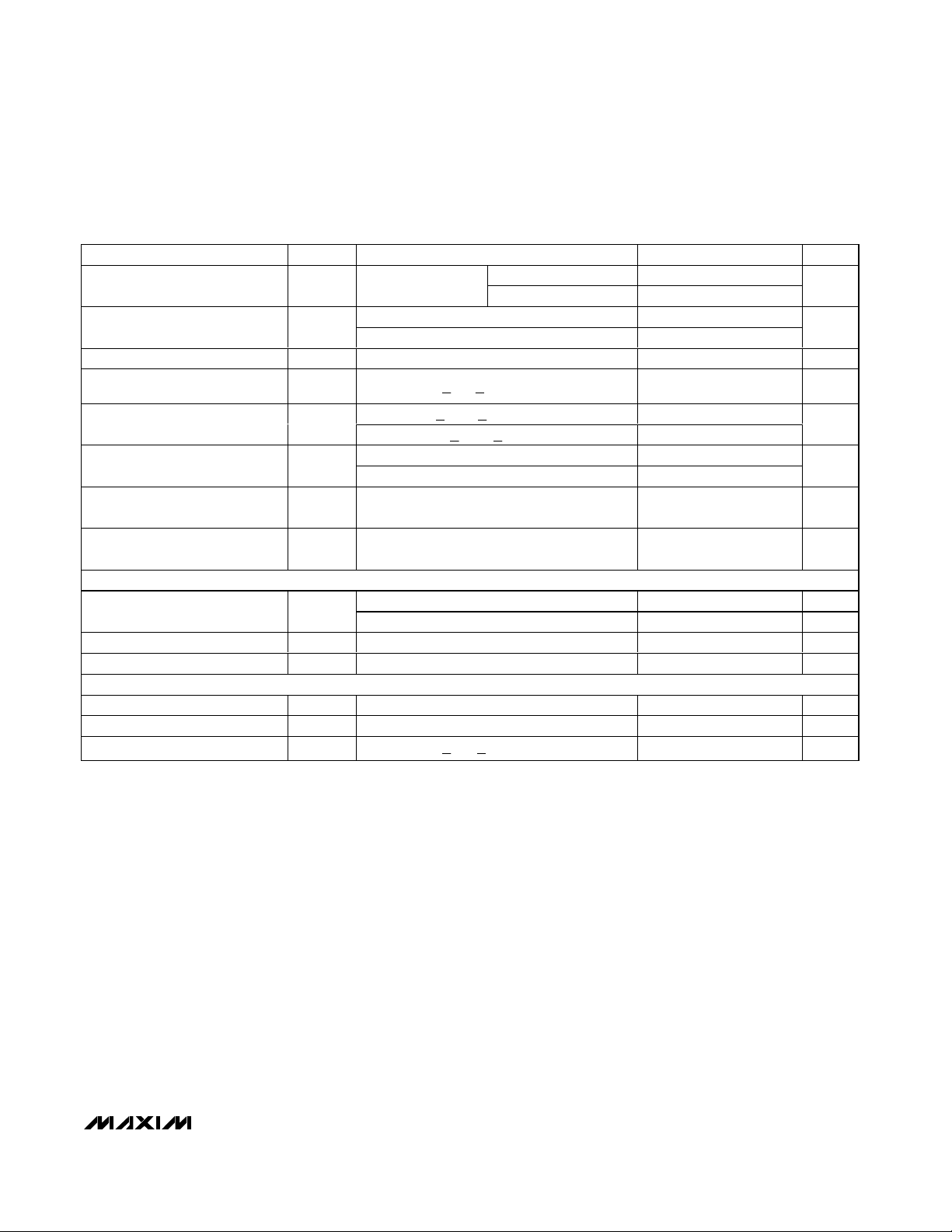
ELECTRICAL CHARACTERISTICS—MAX6161 (V
OUT
= 1.25V)
(VIN= +5V, I
OUT
= 0, TA= T
MIN
to T
MAX
, unless otherwise specified. Typical values are at TA= +25°C.) (Note 1)
PARAMETER
SYMBOL
CONDITIONS
MIN
TYP
MAX
UNITS
MAX6161A
Output Voltage V
OUT
TA = +25°C
MAX6161B
V
MAX6161A 4 10
Output Voltage Temperature
Coefficient (Note 2)
MAX6161B 6 15
ppm/°C
Line Regulation
ΔV
IN
2.5V
<
VIN
<
12.6V 12
µV/V
Sourcing: 0
<
I
OUT
<
4mA 0.5 0.9
Load Regulation
Sinking: -2mA
<
I
OUT
<
0 1.3 2.5
mV/mA
Short to GND 110
OUT Short-Circuit Current I
SC
Short to IN 25
mA
Long-Term Stability
time
1000hr at +25°C 115
ppm/
1000hr
Output Voltage Hysteresis
(Note 3)
cycle
125
ppm
DYNAMIC CHARACTERISTICS
f = 0.1Hz to 10Hz 20
µVp-p
Noise Voltage e
OUT
f = 10Hz to 10kHz 15
µV
RMS
Ripple Rejection
VIN = +5V ±100mV, f = 120Hz 80 dB
Turn-On Settling Time t
R
V
OUT
to 0.1% of final value, C
OUT
= 50pF 50 µs
INPUT CHARACTERISTICS
Supply Voltage Range V
IN
Guaranteed by line-regulation test 2.5
V
Quiescent Supply Current I
IN
125
µA
Change in Supply Current
µA/V
1.248 1.250 1.252
1.246 1.250 1.254
TCV
OUT
ΔV
/
OUT
ΔV
/
OUT
ΔI
OUT
ΔV
/
OUT
ΔV
/
OUT
V
OUT/VIN
ΔIIN/ΔVIN2.5V < VIN < 12.6V 3.2 8.0
150
12.6
150
MAX6161–MAX6168
Precision, Micropower, Low-Dropout, High-
Output-Current, SO-8 Voltage References
_______________________________________________________________________________________ 3
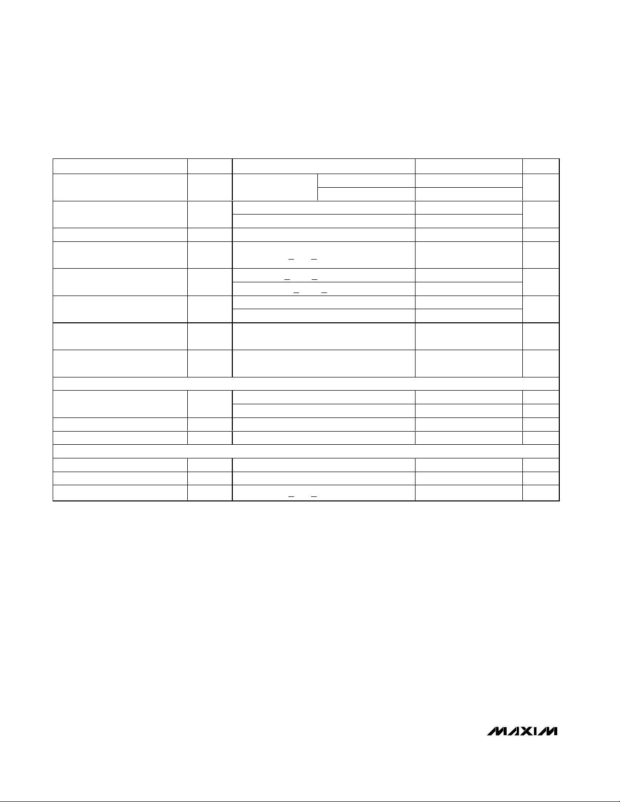
ELECTRICAL CHARACTERISTICS—MAX6168 (V
OUT
= 1.800V)
(VIN= +5V, I
OUT
= 0, TA= T
MIN
to T
MAX
, unless otherwise specified. Typical values are at TA= +25°C.) (Note 1)
PARAMETER
SYMBOL
CONDITIONS
MIN
TYP
MAX
UNITS
MAX6168A
Output Voltage V
OUT
TA = +25°C
MAX6168B
V
MAX6168A 2 5
Output Voltage Temperature
Coefficient (Note 2)
MAX6168B 4 10
ppm/°C
Line Regulation
ΔV
IN
2.5V ≤ VIN ≥ 12.6V 42
µV/V
Sourcing: 0
<
I
OUT
<
5mA 0.5 0.9
Load Regulation
Sinking: -2mA
<
I
OUT
<
0 1.5 4
mV/mA
Short to GND 110
OUT Short-Circuit Current I
SC
Short to IN 25
mA
Long-Term Stability
time
1000hr at +25°C80
ppm/
1000hr
Output Voltage Hysteresis
(Note 3)
cycle
125
ppm
DYNAMIC CHARACTERISTICS
f = 0.1Hz to 10Hz 22
µVp-p
Noise Voltage e
OUT
f = 10Hz to 10kHz 25
µV
RMS
Ripple Rejection
ΔV
IN
VIN = +5V ±100mV, f = 120Hz 78 dB
Turn-On Settling Time t
R
V
OUT
to 0.1% of final value, C
OUT
= 50pF 100 µs
INPUT CHARACTERISTICS
Supply Voltage Range V
IN
Guaranteed by line-regulation test 2.5
V
Quiescent Supply Current I
IN
100
µA
Change in Supply Current
ΔIIN/ΔV
IN
2.5V
<
VIN
<
12.6V 3.4 8.0
µA/V
TCV
OUT
ΔV
/
OUT
ΔV
/
OUT
ΔI
OUT
ΔV
/
OUT
ΔV
/
OUT
ΔV
/
OUT
1.798 1.800 1.802
1.795 1.800 1.805
200
12.6
120
MAX6161–MAX6168
Precision, Micropower, Low-Dropout, HighOutput-Current, SO-8 Voltage References
4 _______________________________________________________________________________________
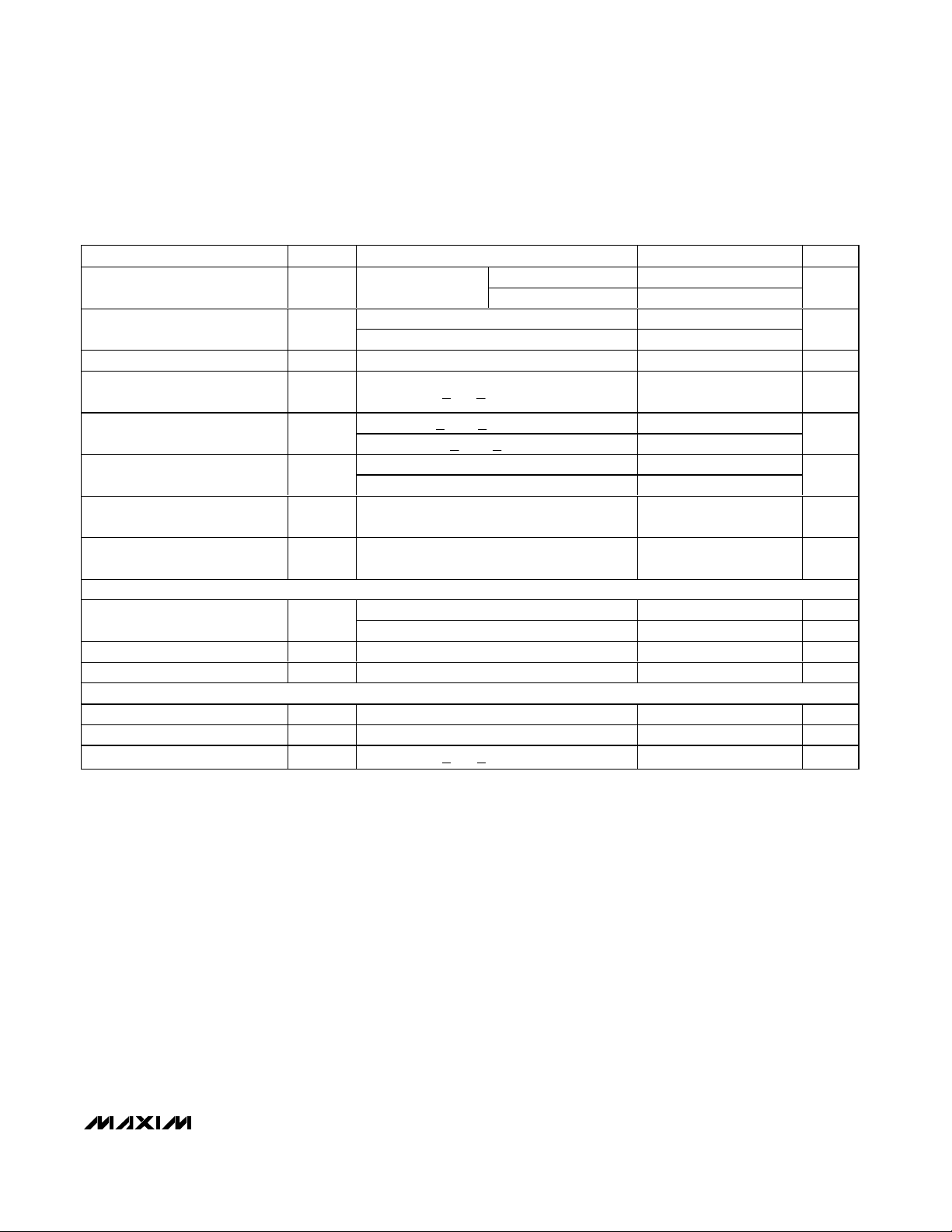
ELECTRICAL CHARACTERISTICS—MAX6162 (V
OUT
= 2.048V)
(VIN= +5V, I
OUT
= 0, TA= T
MIN
to T
MAX
, unless otherwise specified. Typical values are at TA= +25°C.) (Note 1)
PARAMETER
CONDITIONS
UNITS
MAX6162A
Output Voltage V
OUT
TA = +25°C
MAX6162B
V
MAX6162A 2 5
Output Voltage Temperature
Coefficient (Note 2)
MAX6162B 4 10
ppm/°C
Line Regulation
2.5V
<
V
IN
<
12.6V 42 250
µV/V
Sourcing: 0
<
I
OUT
<
5mA 0.5 0.9
Load Regulation
ΔI
OUT
Sinking: -2mA
<
I
OUT
<
0 1.5 4
mV/mA
Short to GND
OUT Short-Circuit Current I
SC
Short to IN 25
mA
Long-Term Stability
time
1000hr at +25°C80
ppm/
1000hr
Output Voltage Hysteresis
(Note 3)
cycle
ppm
DYNAMIC CHARACTERISTICS
f = 0.1Hz to 10Hz 22
µVp-p
Noise Voltage e
OUT
f = 10Hz to 10kHz 25
µV
RM S
Ripple Rejection
VIN = 5V ±100mV, f = 120Hz 78 dB
Turn-On Settling Time t
R
V
OUT
to 0.1% of final value, C
OUT
= 50pF
µs
INPUT CHARACTERISTICS
Supply Voltage Range V
IN
Guaranteed by line-regulation test 2.5
V
Quiescent Supply Current I
IN
120 µA
Change in Supply Current
µA/V
SYMBOL
TCV
OUT
ΔV
/
OUT
ΔV
/
OUT
ΔV
/
OUT
ΔV
/
OUT
V
OUT/VIN
ΔIIN/ΔVIN2.5V < V
IN
MIN TYP MAX
2.046 2.048 2.050
2.043 2.048 2.053
110
125
100
12.6
100
< 12.6V 3.4 8.0
MAX6161–MAX6168
Precision, Micropower, Low-Dropout, High-
Output-Current, SO-8 Voltage References
_______________________________________________________________________________________ 5
ELECTRICAL CHARACTERISTICS—MAX6166 (V
OUT
= 2.500V)
(VIN= +5V, I
OUT
= 0, TA= T
MIN
to T
MAX
, unless otherwise specified. Typical values are at TA= +25°C.) (Note 1)
PARAMETER
SYMBOL
CONDITIONS
MIN
TYP
MAX
UNITS
MAX6166A
Output Voltage V
OUT
TA = +25°C
MAX6166B
V
MAX6166A 2 5
Output Voltage Temperature
Coefficient (Note 2)
MAX6166B 4 10
ppm/°C
Dropout Voltage (Note 4)
I
OUT
= 1mA 50
mV
Line Regulation
ΔV
IN
V
OUT
+ 0.2V
<
V
IN
<
12.6V 60
µV/V
Sourcing: 0
<
I
OUT
<
5mA 0.5 0.9
Load Regulation
Sinking: -2mA
<
I
OUT
<
0 1.6 5
mV/mA
Short to GND 110
OUT Short-Circuit Current I
SC
Short to IN 25
mA
Long-Term Stability
time
1000hr at +25°C80
ppm/
1000hr
Output Voltage Hysteresis
(Note 3)
cycle
125
ppm
DYNAMIC CHARACTERISTICS
f = 0.1Hz to 10Hz 27
µVp-p
Noise Voltage e
OUT
f = 10Hz to 10kHz 30
µV
RMS
Ripple Rejection
VIN = 5V ±100mV, f = 120Hz 76 dB
Turn-On Settling Time t
R
V
OUT
to 0.1% of final value, C
OUT
= 50pF 115 µs
INPUT CHARACTERISTICS
Supply Voltage Range V
IN
Guaranteed by line-regulation test
V
Quiescent Supply Current I
IN
100
µA
Change in Supply Current
V
OUT
+ 0.2V
<
VIN
<
12.6V 3.2 8.0
µA/V
TCV
OUT
VIN - V
OUT
ΔV
/
OUT
ΔV
/
OUT
ΔI
OUT
ΔV
/
OUT
ΔV
/
OUT
V
OUT/VIN
2.498 2.500 2.502
2.495 2.500 2.505
200
250
V
+ 0.2 12.6
OUT
ΔIIN/ΔV
IN
120
MAX6161–MAX6168
Precision, Micropower, Low-Dropout, HighOutput-Current, SO-8 Voltage References
6 _______________________________________________________________________________________
ELECTRICAL CHARACTERISTICS—MAX6163 (V
OUT
= 3.000V)
(VIN= +5V, I
OUT
= 0, TA= T
MIN
to T
MAX
, unless otherwise specified. Typical values are at TA= +25°C.) (Note 1)
PARAMETER
SYMBOL
CONDITIONS
MIN
TYP
MAX
UNITS
MAX6163A
Output Voltage V
OUT
TA = +25°C
MAX6163B
V
MAX6163A 2 5
Output Voltage Temperature
Coefficient (Note 2)
MAX6163B 4 10
ppm/°C
Dropout Voltage (Note 4)
I
OUT
= 1mA 50 200 mV
Line Regulation
ΔV
IN
V
OUT
+ 0.2V
<
VIN
<
12.6V 83 300
µV/V
Sourcing: 0
<
I
OUT
<
5mA 0.5 0.9
Load Regulation
ΔI
OUT Sinking: -2mA
<
I
OUT
<
0 1.8 5
mV/mA
Short to GND
OUT Short-Circuit Current I
SC
Short to IN 25
mA
Long-Term Stability
time
1000hr at +25°C80
ppm/
1000hr
Output Voltage Hysteresis
(Note 3)
cycle
ppm
DYNAMIC CHARACTERISTICS
f = 0.1Hz to 10Hz 35
µVp-p
Noise Voltage e
OUT
f = 10Hz to 10kHz 40
µV
RMS
Ripple Rejection
VIN = 5V ±100mV, f = 120Hz 76 dB
Turn-On Settling Time t
R
V
OUT
to 0.1% of final value, C
OUT
= 50pF
µs
INPUT CHARACTERISTICS
Supply Voltage Range V
IN
Guaranteed by line-regulation test V
OUT
+ 0.2
V
Quiescent Supply Current I
IN
120 µA
Change in Supply Current
V
OUT
+ 0.2V
<
VIN
<
12.6V 3.2 8.0
µA/V
TCV
OUT
VIN - V
OUT
ΔV
/
OUT
ΔV
/
OUT
ΔV
/
OUT
ΔV
/
OUT
V
OUT/VIN
2.998 3.000 3.002
2.995 3.000 3.005
110
125
115
ΔIIN/ΔV
IN
12.6
100
MAX6161–MAX6168
Precision, Micropower, Low-Dropout, High-
Output-Current, SO-8 Voltage References
_______________________________________________________________________________________ 7
ELECTRICAL CHARACTERISTICS—MAX6164 (V
OUT
= 4.096V)
(VIN= +5V, I
OUT
= 0, TA= T
MIN
to T
MAX
, unless otherwise specified. Typical values are at TA= +25°C.) (Note 1)
PARAMETER
SYMBOL
CONDITIONS
MIN
TYP
MAX
UNITS
MAX6164A
Output Voltage V
OUT
TA = +25°C
MAX6164B
V
MAX6164A 2 5
Output Voltage Temperature
Coefficient (Note 2)
MAX6164B 4 10
ppm/°C
Dropout Voltage (Note 4)
I
OUT
= 1mA 50 200 mV
Line Regulation
ΔV
IN
V
OUT
+ 0.2V
<
V
IN
<
12.6V
300
µV/V
Sourcing: 0
<
I
OUT
<
5mA 0.6 0.9
Load Regulation
Sinking: -2mA
<
I
OUT
<
0 2.0 7.0
mV/mA
Short to GND
OUT Short-Circuit Current I
SC
Short to IN 25
mA
Long-Term Stability
time
1000hr at +25°C80
ppm/
1000hr
Output Voltage Hysteresis
(Note 3)
cycle
ppm
DYNAMIC CHARACTERISTICS
f = 0.1Hz to 10Hz 50
µVp-p
Noise Voltage e
OUT
f = 10Hz to 10kHz 50
µV
RMS
Ripple Rejection
VIN = 5V ±100mV, f = 120Hz 72 dB
Turn-On Settling Time t
R
V
OUT
to 0.1% of final value, C
OUT
= 50pF
µs
INPUT CHARACTERISTICS
Supply Voltage Range V
IN
Guaranteed by line-regulation test V
OUT
+ 0.2
V
Quiescent Supply Current I
IN
120 µA
Change in Supply Current
V
OUT
+ 0.2V
<
VIN
<
12.6V 3.2 8.0
µA/V
TCV
OUT
VIN - V
OUT
ΔV
/
OUT
ΔV
/
OUT
ΔI
OUT
ΔV
/
OUT
ΔV
/
OUT
V
OUT/VIN
4.094 4.096 4.098
4.091 4.096 4.101
140
110
125
190
ΔIIN/ΔV
IN
100
12.6

MAX6161–MAX6168
Precision, Micropower, Low-Dropout, HighOutput-Current, SO-8 Voltage References
8 _______________________________________________________________________________________
ELECTRICAL CHARACTERISTICS—MAX6167 (V
OUT
= 4.500V)
(VIN= +5V, I
OUT
= 0, TA= T
MIN
to T
MAX
, unless otherwise specified. Typical values are at TA= +25°C.) (Note 1)
PARAMETER
SYMBOL
CONDITIONS
MIN
TYP
MAX
UNITS
MAX6167A
Output Voltage V
OUT
TA = +25°C
MAX6167B
V
MAX6167A 2 5
Output Voltage Temperature
Coefficient (Note 2)
MAX6167B 4 10
Dropout Voltage (Note 4)
I
OUT
= 1mA 50
mV
Line Regulation
ΔV
IN
V
OUT
+ 0.2V
<
VIN
<
12.6V
Sourcing: 0
<
I
OUT
<
5mA 0.6 0.9
Load Regulation
Sinking: -2mA
<
I
OUT
<
0 2.3 8.0
Short to GND
OUT Short-Circuit Current I
SC
Short to IN 25
mA
Long-Term Stability
time
1000hr at +25°C80
Output Voltage Hysteresis
(Note 3)
cycle
DYNAMIC CHARACTERISTICS
f = 0.1Hz to 10Hz 55
Noise Voltage e
OUT
f = 10Hz to 10kHz 55
Ripple Rejection
VIN = 5V ±100mV, f = 120Hz 70 dB
Turn-On Settling Time t
R
V
OUT
to 0.1% of final value, C
OUT
= 50pF
µs
INPUT CHARACTERISTICS
Supply Voltage Range V
IN
Guaranteed by line-regulation test V
OUT
+ 0.2
V
Quiescent Supply Current I
IN
µA
Change in Supply Current
V
OUT
+ 0.2V
<
VIN
<
12.6V 3.1 8.0
TCV
OUT
VIN - V
OUT
ΔV
/
OUT
ΔV
/
OUT
ΔI
OUT
ΔV
/
OUT
Δ
V
OUT/
V
OUT/VIN
4.498 4.500 4.502
4.495 4.500 4.505
200
160 450 µV/V
110
125 ppm
230
ppm/°C
mV/mA
ppm/
1000hr
µVp-p
µV
RMS
12.6
µA/V
ΔIIN/ΔV
IN
100 120

MAX6161–MAX6168
Precision, Micropower, Low-Dropout, High-
Output-Current, SO-8 Voltage References
_______________________________________________________________________________________ 9
ELECTRICAL CHARACTERISTICS—MAX6165 (V
OUT
= 5.000V)
(VIN= +5.5V, I
OUT
= 0, TA= T
MIN
to T
MAX
, unless otherwise specified. Typical values are at TA= +25°C.) (Note 1)
PARAMETER
SYMBOL
CONDITIONS
MIN
TYP
MAX
UNITS
MAX6165A
Output Voltage V
OUT
TA = +25°C
MAX6165B
V
MAX6165A 2 5
Output Voltage Temperature
Coefficient (Note 2)
MAX6165B 4 10
ppm/°C
Dropout Voltage (Note 4)
I
OUT
= 1mA 50
mV
Line Regulation
V
OUT
+ 0.2V
<
VIN
<
12.6V
µV/V
Sourcing: 0
<
I
OUT
<
5mA 0.6 0.9
Load Regulation
ΔI
OUT Sinking: -2mA
<
I
OUT
<
0 2.4 8.0
mV/mA
Short to GND
OUT Short-Circuit Current I
SC
Short to IN 25
mA
Long-Term Stability
time
1000hr at +25°C80
ppm/
1000hr
Output Voltage Hysteresis
(Note 3)
cycle
ppm
DYNAMIC CHARACTERISTICS
f = 0.1Hz to 10Hz 60
µVp-p
Noise Voltage e
OUT
f = 10Hz to 10kHz 60
µV
RMS
Ripple Rejection
VIN = 5.5V ±100mV, f = 120Hz 65 dB
Turn-On Settling Time t
R
V
OUT
to 0.1% of final value, C
OUT
= 50pF
µs
INPUT CHARACTERISTICS
Supply Voltage Range V
IN
Guaranteed by line-regulation test V
OUT
+ 0.2
V
Quiescent Supply Current I
IN
µA
Change in Supply Current
V
OUT
+ 0.2V
<
VIN
<
12.6V 3.1 8.0
µA/V
Note 1: 100% production tested at TA= +25°C. Guaranteed by design for TA= -40°C to +85°C.
Note 2: Temperature Coefficient is specified by the “box” method; i.e., the maximum ΔV
OUT
is divided by the maximum ΔT.
Note 3: Thermal Hysteresis is defined as the change in T
A
= +25°C output voltage before and after temperature cycling of the
device (from T
A
= T
MIN
to T
MAX
). Initial measurement at TA= +25°C is followed by temperature cycling the device to
TA= +85°C then to TA= -40°C, and another measurement at TA= +25°C is compared to the original measurement at
TA= +25°C.
Note 4: Dropout voltage is the minimum input voltage at which V
OUT
changes ≤ 0.2% from V
OUT
at VIN= 5.0V (VIN= 5.5V for
MAX6165).
TCV
OUT
VIN - V
OUT
ΔV
/
OUT
ΔV
/
OUT
ΔV
/
OUT
ΔV
/
OUT
V
OUT/VIN
4.998 5.000 5.002
4.995 5.000 5.005
200
180 400
110
125
300
ΔIIN/ΔV
IN
100 120
12.6

MAX6161–MAX6168
Precision, Micropower, Low-Dropout, HighOutput-Current, SO-8 Voltage References
10 ______________________________________________________________________________________
Typical Operating Characteristics
(VIN= +5V for MAX6161–MAX6168, VIN= +5.5V for MAX6165, I
OUT
= 0, TA= +25°C, unless otherwise noted.) (Note 5)
MAX6161
OUTPUT VOLTAGE TEMPERATURE DRIFT
MAX6161/68 toc01
TEMPERATURE (°C)
OUTPUT VOLTAGE (V)
705525 40-10 0 10-25
1.2496
1.2497
1.2498
1.2499
1.2500
1.2501
1.2502
1.2503
1.2504
1.2505
1.2495
-40 85
3 TYPICAL PARTS
MAX6165
OUTPUT VOLTAGE TEMPERATURE DRIFT
MAX6161/68 toc02
TEMPERATURE (°C)
OUTPUT VOLTAGE (V)
7055-25 -10 0 2510 40
4.9985
4.9990
4.9995
5.0000
5.0005
5.0010
5.0015
5.0020
4.9980
-40 85
3 TYPICAL PARTS
MAX6161
LONG-TERM DRIFT
MAX6161/68 toc03
TIME (hrs)
DRIFT (ppm)
768
192
384
576
-30
-20
-10
0
10
20
30
40
50
60
-40
0 960
MAX6165
LONG-TERM DRIFT
MAX6161/68 toc04
TIME (hrs)
DRIFT (ppm)
768
192
384
576
-90
-80
-70
-60
-50
-40
-30
-20
-10
0
-100
0960
-300
-200
-100
0
100
200
300
2 4 6 8 10 12
MAX6161
LINE REGULATION
MAX6161/68 toc05
INPUT VOLTAGE (V)
OUTPUT VOLTAGE CHANGE (μV)
TA = +85°C
TA = +25°C
TA = -40°C
-1200
-600
-800
-1000
-400
-200
0
200
5971113
MAX6165
LINE REGULATION
MAX6161/68 toc06
INPUT VOLTAGE (V)
OUTPUT VOLTAGE CHANGE (μV)
TA = +85°C
TA = +25°C
TA = -40°C
-3
1
0
-1
-2
2
3
4
5
-4 -2 0 2 4
MAX6161/68 toc07
LOAD CURRENT (mA)
OUTPUT VOLTAGE CHANGE (mV)
TA = +25°C
TA = -40°C
MAX6161
LOAD REGULATION
TA = +85°C
-6
2
0
-2
-4
4
8
6
10
12
-6 -2-4 0246
MAX6161/68 toc08
LOAD CURRENT (mA)
OUTPUT VOLTAGE CHANGE (mV)
MAX6165
LOAD REGULATION
TA = +25°C
TA = +85°C
TA = -40°C
0
0.10
0.05
0.20
0.15
0.25
0.30
021345
MAX6166
DROPOUT VOLTAGE
vs. LOAD CURRENT
MAX6161/68 toc09
LOAD CURRENT (mA)
DROPOUT VOLTAGE (V)
TA = +85°C
TA = +25°C
TA = -40°C

MAX6161–MAX6168
Precision, Micropower, Low-Dropout, High-
Output-Current, SO-8 Voltage References
______________________________________________________________________________________ 11
Typical Operating Characteristics (continued)
(VIN= +5V for MAX6161–MAX6168, VIN= +5.5V for MAX6165, I
OUT
= 0, TA= +25°C, unless otherwise noted.) (Note 5)
0
0.05
0.15
0.10
0.20
0.25
021345
TA = +85°C
TA = +25°C
TA = -40°C
MAX6161/68 toc10
LOAD CURRENT (mA)
DROPOUT VOLTAGE (V)
MAX6165
DROPOUT VOLTAGE
vs. LOAD CURRENT
MAX6161/68 toc11
FREQUENCY (kHz)
PSRR (dB)
0
-10
-20
-30
-40
-50
-60
-70
-80
-90
0.001 1 10 1000.01 0.1 1000
MAX6161
POWER-SUPPLY REJECTION RATIO
vs. FREQUENCY
-70
-80
0.001 10 1000
-60
-50
-40
-30
-20
-10
0
FREQUENCY (kHz)
PSRR (dB)
0.1
MAX6165
POWER-SUPPLY REJECTION RATIO
vs. FREQUENCY
MAX6161/68 toc12
MAX6161
SUPPLY CURRENT vs. SUPPLY VOLTAGE
MAX6161/68 toc13
SUPPLY VOLTAGE (V)
SUPPLY CURRENT (μA)
1210864
108
116
124
132
140
148
156
164
172
180
100
214
TA = +85°C
TA = +25°C
TA = -40°C
MAX6165
SUPPLY CURRENT vs. SUPPLY VOLTAGE
MAX6161/68 toc14
SUPPLY VOLTAGE (V)
SUPPLY CURRENT (μA)
131210 117 8 96
96
102
108
114
120
126
132
138
144
150
90
514
TA = +85°C
TA = +25°C
TA = -40°C
MAX6161
SUPPLY CURRENT vs. TEMPERATURE
MAX6161/68 toc15
TEMPERATURE (°C)
SUPPLY CURRENT (μA)
603510-15
108
116
124
132
140
148
156
164
172
180
100
-40 85
VCC = +12.6V
VCC = +5V
VCC = +2.5V
MAX6165
SUPPLY CURRENT vs. TEMPERATURE
MAX6161/68 toc16
TEMPERATURE (°C)
SUPPLY CURRENT (μA)
603510-15
96
102
108
114
120
126
132
138
144
150
90
-40 85
VCC = +12.6V
VCC = +5.2V
0
0.001 10 1000
40
20
60
80
100
140
120
160
180
200
220
MAX6161/68 toc17
FREQUENCY (kHz)
OUTPUT IMPEDANCE (Ω)
0.1
MAX6161
OUTPUT IMPEDANCE
vs. FREQUENCY
180
0
0.001 10 1000
40
20
60
100
80
120
140
160
MAX6161/68 toc18
FREQUENCY (kHz)
OUTPUT IMPEDANCE (Ω)
0.1
MAX6165
OUTPUT IMPEDANCE
vs. FREQUENCY

MAX6161–MAX6168
Precision, Micropower, Low-Dropout, HighOutput-Current, SO-8 Voltage References
12 ______________________________________________________________________________________
Typical Operating Characteristics (continued)
(VIN= +5V for MAX6161–MAX6168, VIN= +5.5V for MAX6165, I
OUT
= 0, TA= +25°C, unless otherwise noted.) (Note 5)
V
OUT
10μV/div
1s/div
MAX6161
0.1Hz TO 10Hz OUTPUT NOISE
MAX6161/68 toc19
V
OUT
10μV/div
1s/div
MAX6165
NOISE
MAX6161/68 toc20
V
OUT
500mV/div
V
IN
5V/div
10μs/div
MAX6161
TURN-ON TRANSIENT
(C
L
= 50pF)
MAX6161/68 toc21
V
OUT
2V/div
V
IN
5V/div
40μs/div
MAX6165
TURN-ON TRANSIENT
(C
L
= 50pF)
MAX6161/67 toc22
I
OUT
500μA/div
V
OUT
AC-COUPLED
100mV/div
400μs/div
MAX6161
LOAD TRANSIENT
(I
OUT
= ±250μA, V
IN
= 5.0, CL = 0)
+250μA
-250μA
MAX6161/68 toc23
I
OUT
500μA/div
V
OUT
AC-COUPLED
50mV/div
400μs/div
MAX6165
LOAD TRANSIENT
(I
OUT
= ±250μA, CL = 0, V
IN
= 5.5V)
+250μA
-250μA
MAX6161/68 toc24

MAX6161–MAX6168
Precision, Micropower, Low-Dropout, High-
Output-Current, SO-8 Voltage References
______________________________________________________________________________________ 13
I
OUT
5mA/div
V
OUT
AC-COUPLED
50mV/div
400μs/div
MAX6165
LOAD TRANSIENT
(C
L
= 0, I
OUT
= ±2mA, V
IN
= 5.5V)
+2mA
-2mA
MAX6161/68 toc28
I
OUT
5mA/div
V
OUT
AC-COUPLED
100mV/div
400μs/div
MAX6161
LOAD TRANSIENT
(V
IN
= 5.0V, CL = 0, I
OUT
= ±2mA)
+2mA
-2mA
MAX6161/68 toc27
I
OUT
5mA/div
V
OUT
AC-COUPLED
50mV/div
400μs/div
MAX6161
LOAD TRANSIENT
(V
IN
= 5.0V, CL = 1μF, I
OUT
= ±2mA)
+2mA
-2mA
MAX6161/68 toc29
I
OUT
5mA/div
V
OUT
AC-COUPLED
20mV/div
400μs/div
MAX6165
LOAD TRANSIENT
(C
L
= 1μF, I
OUT
= ±2mA, V
IN
= 5.5V)
+2mA
-2mA
MAX6161/68 toc30
I
OUT
500μA/div
V
OUT
AC-COUPLED
10mV/div
400μs/div
MAX6161
LOAD TRANSIENT
(I
OUT
= ±250μA, V
IN
= 5.0V, CL = 1μF)
+250μA
-250μA
MAX6161/68 toc25
I
OUT
500μA/div
V
OUT
AC-COUPLED
20mV/div
400μs/div
MAX6165
LOAD TRANSIENT
(I
OUT
= ±250μA, CL = 1μF, V
IN
= 5.5V)
+250μA
-250μA
MAX6161/68 toc26
Typical Operating Characteristics (continued)
(VIN= +5V for MAX6161–MAX6168, VIN= +5.5V for MAX6165, I
OUT
= 0, TA= +25°C, unless otherwise noted.) (Note 5)

MAX6161–MAX6168
Precision, Micropower, Low-Dropout, HighOutput-Current, SO-8 Voltage References
14 ______________________________________________________________________________________
I
OUT
5mA/div
V
OUT
AC-COUPLED
50mV/div
400μs/div
MAX6161
LOAD TRANSIENT
(V
IN
= 5.0V, CL = 1μF, I
OUT
= ±4mA)
+4mA
-4mA
MAX6161/68 toc33
I
OUT
5mA/div
V
OUT
AC-COUPLED
50mV/div
400μs/div
MAX6165
LOAD TRANSIENT
(I
OUT
= ±5mA, CL = 1μF, V
IN
= 5.5V)
+5mA
-5mA
MAX6161/68 toc34
V
IN
500mV/div
V
OUT
AC-COUPLED
20mV/div
40μs/div
MAX6161
LINE TRANSIENT
(C
L
= 0)
+0.25V
-0.25V
MAX6161/68 toc35
V
IN
500mV/div
V
OUT
AC-COUPLED
20mV/div
40μs/div
MAX6165
LINE TRANSIENT
(C
L
= 0)
+0.25V
-0.25V
MAX6161/68 toc36
Note 5: Many of the Typical Operating Characteristics of the MAX6161 family are extremely similar. The extremes of these characteristics
are found in the MAX6161 (1.25V output) and the MAX6165 (5.0V output). The Typical Operating Characteristics of the remainder of the MAX6161 family typically lie between these two extremes and can be estimated based on their output voltages.
Typical Operating Characteristics (continued)
(VIN= +5V for MAX6161–MAX6168, VIN= +5.5V for MAX6165, I
OUT
= 0, TA= +25°C, unless otherwise noted.) (Note 5)
I
OUT
5mA/div
V
OUT
AC-COUPLED
200mV/div
400μs/div
MAX6161
LOAD TRANSIENT
(V
IN
= 5.0V, CL = 0, I
OUT
= ±4mA)
+4mA
-4mA
MAX6161/68 toc31
I
OUT
5mA/div
V
OUT
AC-COUPLED
100mV/div
400μs/div
MAX6165
LOAD TRANSIENT
(I
OUT
= ±5mA, CL = 0, V
IN
= 5.5V)
+5mA
-5mA
MAX6161/68 toc32
MAX6161–MAX6168
Precision, Micropower, Low-Dropout, High-
Output-Current, SO-8 Voltage References
______________________________________________________________________________________ 15
Applications Information
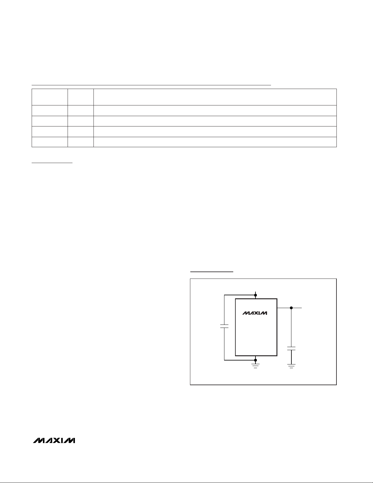
Input Bypassing
For the best line-transient performance, decouple the
input with a 0.1µF ceramic capacitor as shown in the
Typical Operating Circuit. Locate the capacitor as
close to IN as possible. When transient performance is
less important, no capacitor is necessary.
Output/Load Capacitance
Devices in the MAX6161 family do not require an output
capacitor for frequency stability. In applications where
the load or the supply can experience step changes,
an output capacitor of at least 0.1µF will reduce the
amount of overshoot (undershoot) and improve the circuit’s transient response. Many applications do not
require an external capacitor, and the MAX6161 family
can offer a significant advantage in applications when
board space is critical.
Supply Current
The quiescent supply current of the series-mode
MAX6161 family is typically 100µA and is virtually independent of the supply voltage, with only an 8µA/V
(max) variation with supply voltage. Unlike series references, shunt-mode references operate with a series
resistor connected to the power supply. The quiescent
current of a shunt-mode reference is thus a function of
the input voltage. Additionally, shunt-mode references
have to be biased at the maximum expected load current, even if the load current is not present at the time.
In the MAX6161 family, the load current is drawn from
the input voltage only when required, so supply current
is not wasted and efficiency is maximized at all input
voltages. This improved efficiency reduces power dissipation and extends battery life.
When the supply voltage is below the minimum specified input voltage (as during turn-on), the devices can
draw up to 400µA beyond the nominal supply current.
The input voltage source must be capable of providing
this current to ensure reliable turn-on.
Output Voltage Hysteresis
Output voltage hysteresis is the change in the input
voltage at TA= +25°C before and after the device is
cycled over its entire operating temperature range.
Hysteresis is caused by differential package stress
appearing across the bandgap core transistors. The
typical temperature hysteresis value is 125ppm.
Turn-On Time
These devices typically turn on and settle to within
0.1% of their final value in 50µs to 300µs, depending on
the output voltage (see electrical table of part used).
The turn-on time can increase up to 1.5ms with the
device operating at the minimum dropout voltage and
the maximum load.
IN
+SUPPLY INPUT (SEE SELECTOR GUIDE)
OUT REFERENCE
OUT
1μF*
*CAPACITORS ARE OPTIONAL.
GND
MAX6161–
MAX6168
0.1μF*
Typical Operating Circuit
__________________________Chip Information
TRANSISTOR COUNT: 117
PROCESS: BiCMOS
Pin Description
PIN NAME FUNCTION
No Connection. Not internally connected.N.C.1, 3, 5, 7, 8
2 IN Input Voltage
GroundGND4
6 OUT Reference Output

MAX6161–MAX6168
Precision, Micropower, Low-Dropout, HighOutput-Current, SO-8 Voltage References
16 ______________________________________________________________________________________
Selector Guide
PART
OUTPUT VOLTAGE
(V)
INITIAL ACCURACY
(mV)
TEMPERATURE
COEFFICIENT
(ppm/°C)
MAX6161A 1.250 ±210
MAX6161B 1.250 ±415
MAX6168A 1.800 ±25
MAX6168B 1.800 ±510
MAX6162A 2.048 ±25
MAX6162B 2.048 ±510
MAX6166A 2.500 ±25
MAX6166B 2.500 ±510
MAX6163A 3.000 ±25
MAX6163B 3.000 ±510
MAX6164A 4.096 ±25
MAX6164B 4.096 ±510
MAX6167A 4.500 ±25
MAX6167B
4.500
±510
MAX6165A 5.000 ±25
MAX6165B
5.000
±510

MAX6161–MAX6168
Maxim cannot assume responsibility for use of any circuitry other than circuitry entirely embodied in a Maxim product. No circuit patent licenses are
implied. Maxim reserves the right to change the circuitry and specifications without notice at any time.
Maxim Integrated Products, 120 San Gabriel Drive, Sunnyvale, CA 94086 408-737-7600 _____________________17
© 2005 Maxim Integrated Products Printed USA is a registered trademark of Maxim Integrated Products, Inc.
SOICN .EPS
PACKAGE OUTLINE, .150" SOIC
1
1
21-0041
B
REV.DOCUMENT CONTROL NO.APPROVAL
PROPRIETARY INFORMATION
TITLE:
TOP VIEW
FRONT VIEW
MAX
0.010
0.069
0.019
0.157
0.010
INCHES
0.150
0.007
E
C
DIM
0.014
0.004
B
A1
MIN
0.053A
0.19
3.80 4.00
0.25
MILLIMETERS
0.10
0.35
1.35
MIN
0.49
0.25
MAX
1.75
0.050
0.016L
0.40 1.27
0.3940.386D
D
MINDIM
D
INCHES
MAX
9.80 10.00
MILLIMETERS
MIN
MAX
16
AC
0.337 0.344 AB8.758.55 14
0.189 0.197 AA5.004.80 8
N MS012
N
SIDE VIEW
H 0.2440.228 5.80 6.20
e 0.050 BSC 1.27 BSC
C
HE
e
B
A1
A
D
0∞-8∞
L
1
VARIATIONS:
Precision, Micropower, Low-Dropout, High-
Output-Current, SO-8 Voltage References
Package Information
(The package drawing(s) in this data sheet may not reflect the most current specifications. For the latest package outline information
go to www.maxim-ic.com/packages
.)
 Loading...