

General Description
The MAX6125/MAX6141/MAX6145/MAX6150/MAX6160
low-dropout, micropower, three-terminal voltage references offer 2.5V, 4.096V, 4.5V, 5.0V, and adjustable
(1.23V to 12.4V) output voltages, respectively. Low,
200mV dropout makes these devices ideal for 3V and
5V systems. Unlike two-terminal references that waste
battery current and require an external resistor, the
MAX61xx family’s supply current is virtually independent
of input voltage variations, which translates to longer
battery life.
Initial accuracy for these devices is ±1%. The output
temperature coefficient is typically 15ppm/°C, and
guaranteed to be less than 50ppm/°C (except
for the MAX6160). The MAX6125/MAX6141/MAX6145/
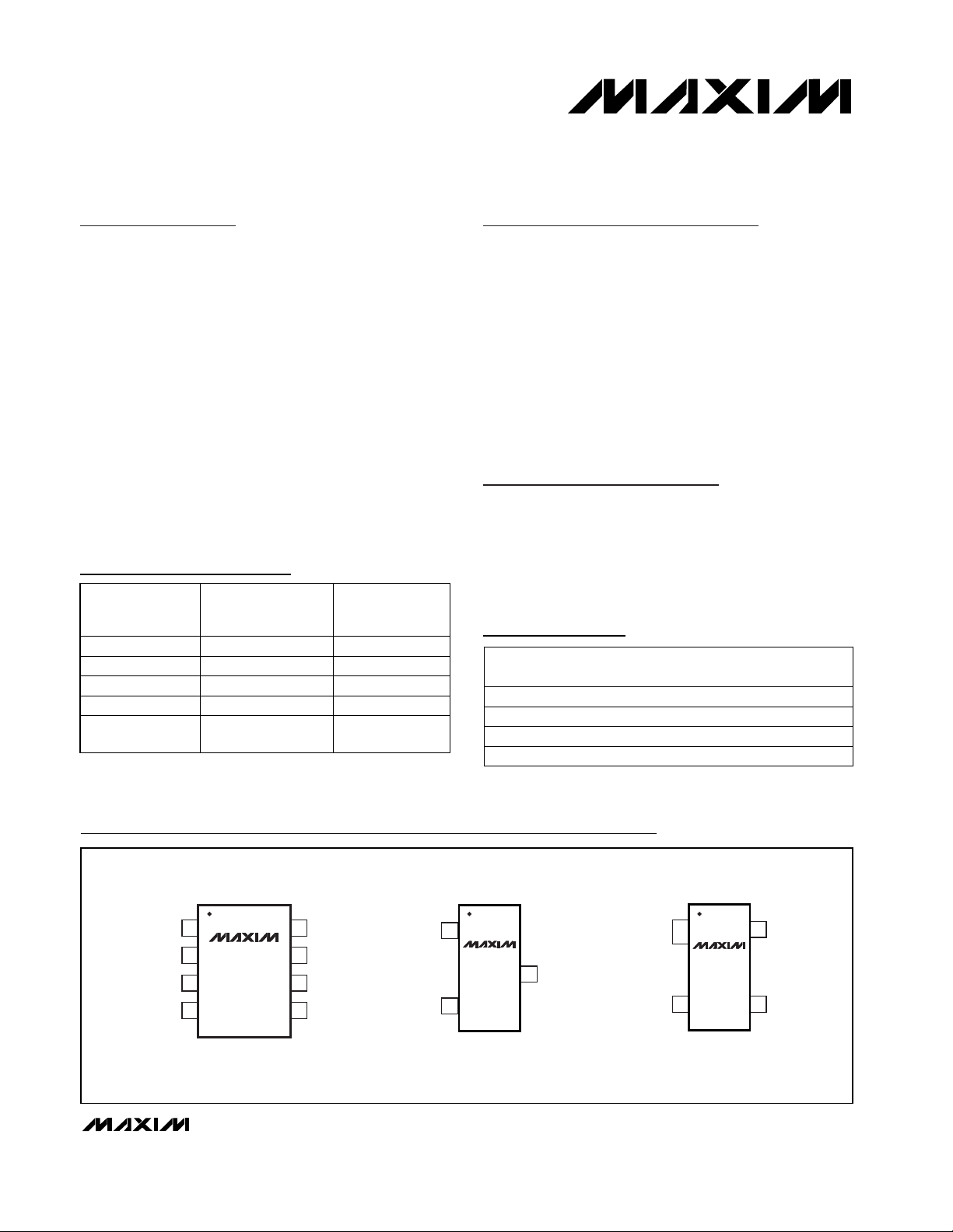
MAX6150 are available in 3-pin SOT23 and 8-pin SO
packages. The MAX6160 is available in 4-pin SOT143
and 8-pin SO packages.
Features
♦ 3-Pin SOT23 Package
(MAX6125/MAX6141/MAX6145/MAX6150)
4-Pin SOT143 Package (MAX6160)
♦ Low, 200mV Dropout Voltage
♦ 75µA Supply Current, Independent of
Input Voltage
♦ 15ppm/°C Typical Tempco (50ppm/°C, max)
♦ Stable for All Capacitive Loads up to 10nF
♦ Adjustable Output Voltage from
1.23V to (VIN- 0.2V) (MAX6160)
♦ Optimized for 3V/5V Operation
Applications
3V/5V Systems
Battery-Powered Systems
Portable and Hand-Held Equipment
Data-Acquisition Systems
Instrumentation and Process Control
MAX6125/MAX6141/MAX6145/MAX6150/MAX6160
SOT23, Low-Cost, Low-Dropout,
3-Terminal Voltage References
________________________________________________________________ Maxim Integrated Products 1
Pin Configurations
PART
MAX6125ESA
MAX6125EUR-T -40°C to +85°C
-40°C to +85°C
TEMP
RANGE
PINPACKAGE
8 SO
3 SOT23-3
Ordering Information
Selector Guide
For pricing, delivery, and ordering information, please contact Maxim/Dallas Direct! at
1-888-629-4642, or visit Maxim’s website at www.maxim-ic.com.
TOP
MARK
—
EBAA
PART
MAX6125
MAX6141
MAX6145
MAX6150
4.096
2.5
PRESET OUTPUT
VOLTAGE (V)
PINPACKAGE
3 SOT23/8 SO
3 SOT23/8 SO
5
4.5 3 SOT23/8 SO
3 SOT23/8 SO
MAX6160
Adjustable
(1.23 to 12.40)
4 SOT143/8 SO
19-1177; Rev. 1; 10/02
Ordering Information continued on last page.
Typical Operating Circuit appears on last page.
MAX6141ESA
-40°C to +85°C 8 SO —
MAX6141EUR-T -40°C to +85°C 3 SOT23-3 ECAA
TOP VIEW
1
OUT
MAX6125
2
N.C.
N.C.
GND
( ) ARE FOR MAX6160 ONLY
MAX6141
MAX6145
3
MAX6150
MAX6160
4
SO
8
7
6
5
IN
N.C.
N.C.
N.C. (ADJ)
OUT
IN
1
MAX6125
MAX6141
MAX6145
MAX6150
2
SOT23-3
4
GND
1
MAX6160
GND
3
2
ADJ
SOT143-4
OUT
3
IN
MAX6125/MAX6141/MAX6145/MAX6150/MAX6160
SOT23, Low-Cost, Low-Dropout,
3-Terminal Voltage References
2 _______________________________________________________________________________________
ABSOLUTE MAXIMUM RATINGS
ELECTRICAL CHARACTERISTICS—MAX6125
(VIN= 2.7V, I
OUT
= 0mA, TA= +25°C, unless otherwise noted.) (Note 1)
Stresses beyond those listed under “Absolute Maximum Ratings” may cause permanent damage to the device. These are stress ratings only, and functional
operation of the device at these or any other conditions beyond those indicated in the operational sections of the specifications is not implied. Exposure to
absolute maximum rating conditions for extended periods may affect device reliability.
(Voltages With Respect to GND)
IN.......................................................................-0.3V to +13.5V
OUT, ADJ...................................................-0.3V to (V
IN
+ 0.3V)
Output Short-Circuit Duration (to IN or GND).............Continuous
Continuous Power Dissipation (T
A
= +70°C)
8-Pin SO (derate 5.9mW/°C above +70°C)....................471mW
3-Pin SOT23 (derate 4mW/°C above +70°C).................320mW
4-Pin SOT143 (derate 4mW/°C above +70°C)...............320mW
Operating Temperature Range ...........................-40°C to +85°C
Storage Temperature Range .............................-65°C to +160°C
Lead Temperature (soldering, 10s) .................................+300°C
T
A
= T
MIN
to T
MAX
TA= +25°C
TA= T
MIN
to T
MAX
TA= T
MIN
to T
MAX
TA= +25°C
I
SINK
= 0mA to 1mA
I
SOURCE
= 0mA to 1mA
TA= T
MIN
to T
MAX
0.1Hz to 10Hz
10Hz to 10kHz
VIN= 2.7V to 12.6V, TA= T
MIN
to T
MAX
VIN= 2.7V to 12.6V
CONDITIONS
µA/V1.7 6∆IQ/∆V
IN
Change in Supply Current
vs. Change in Input Voltage
V
2.450 2.550
V
OUT
Output Voltage
2.475 2.500 2.525
V2.7 12.6V
IN
Supply Voltage
µA
130
I
Q
Quiescent Supply Current
75 100
mV/mA
1.15 10
∆V
OUT
/∆I
OUT
Load Regulation
0.4 1
ppm/°C15 50TCV
OUT
Output Voltage
Temperature Coefficient
15
µV
P-P
500
e
n
Output Voltage Noise
µV/V150∆V
OUT
/∆V
IN
Line Regulation
UNITSMIN TYP MAXSYMBOLPARAMETER
TA= T
MIN
to T
MAX
TA= +25°C
TA= T
MIN
to T
MAX
TA= T
MIN
to T
MAX
TA= +25°C
I
SINK
= 0mA to 1mA
I
SOURCE
= 0mA to 1mA
TA= T
MIN
to T
MAX
0.1Hz to 10Hz
10Hz to 10kHz
VIN= 4.3V to 12.6V, TA= T
MIN
to T
MAX
VIN= 4.3V to 12.6V
CONDITIONS
µA/V1.7 6∆IQ/∆V
IN
Change in Supply Current
vs. Change in Input Voltage
V
4.015 4.180
V
OUT
Output Voltage
4.055 4.096 4.140
V4.3 12.6V
IN
Supply Voltage
µA
130
I
Q
Quiescent Supply Current
78 105
mV/mA
1.65 16
∆V
OUT
/∆I
OUT
Load Regulation
0.55 1.6
ppm/°C15 50TCV
OUT
Output Voltage
Temperature Coefficient
25
µV
P-P
700
e
n
Output Voltage Noise
µV/V250∆V
OUT
/∆V
IN
Line Regulation
UNITSMIN TYP MAXSYMBOLPARAMETER
ELECTRICAL CHARACTERISTICS—MAX6141
(VIN= 4.3V, I
OUT
= 0mA, TA= +25°C, unless otherwise noted.) (Note 1)
_______________________________________________________________________________________ 3
MAX6125/MAX6141/MAX6145/MAX6150/MAX6160
SOT23, Low-Cost, Low-Dropout,
3-Terminal Voltage References
ELECTRICAL CHARACTERISTICS—MAX6145
(VIN= 4.7V, I
OUT
= 0mA, TA= +25°C, unless otherwise noted.) (Note 1)
TA= T
MIN
to T
MAX
TA= +25°C
TA= T
MIN
to T
MAX
TA= T
MIN
to T
MAX
TA= +25°C
I
SINK
= 0mA to 1mA
I
SOURCE
= 0mA to 1mA
TA= T
MIN
to T
MAX
0.1Hz to 10Hz
10Hz to 10kHz
VIN= 4.7V to 12.6V, TA= T
MIN
to T
MAX
VIN= 4.7V to 12.6V
CONDITIONS
µA/V1.7 6∆IQ/∆V
IN
Change in Supply Current
vs. Change in Input Voltage
V
4.410 4.590
V
OUT
Output Voltage
4.455 4.500 4.545
V4.7 12.6V
IN
Supply Voltage
µA
130
I
Q
Quiescent Supply Current
79 105
mV/mA
1.75 18
∆V
OUT
/∆I
OUT
Load Regulation
0.6 1.8
ppm/°C15 50TCV
OUT
Output Voltage
Temperature Coefficient
30
µV
P-P
800
e
n
Output Voltage Noise
µV/V250∆V
OUT
/∆V
IN
Line Regulation
UNITSMIN TYP MAXSYMBOLPARAMETER
TA= T
MIN
to T
MAX
TA= +25°C
TA= T
MIN
to T
MAX
TA= T
MIN
to T
MAX
TA= +25°C
I
SINK
= 0mA to 1mA
I
SOURCE
= 0mA to 1mA
TA= T
MIN
to T
MAX
0.1Hz to 10Hz
10Hz to 10kHz
VIN= 5.2V to 12.6V, TA= T
MIN
to T
MAX
VIN= 5.2V to 12.6V
CONDITIONS
µA/V1.7 6∆IQ/∆V
IN
Change in Supply Current
vs. Change in Input Voltage
V
4.900 5.100
V
OUT
Output Voltage
4.950 5.000 5.050
V5.2 12.6V
IN
Supply Voltage
µA
145
I
Q
Quiescent Supply Current
80 110
mV/mA
1.9 20
∆V
OUT
/∆I
OUT
Load Regulation
0.65 2
ppm/°C15 50TCV
OUT
Output Voltage
Temperature Coefficient
35
µV
P-P
900
e
n
Output Voltage Noise
µV/V150∆V
OUT
/∆V
IN
Line Regulation
UNITSMIN TYP MAXSYMBOLPARAMETER
ELECTRICAL CHARACTERISTICS—MAX6150
(VIN= 5.2V, I
OUT
= 0mA, TA= +25°C, unless otherwise noted.) (Note 1)

__________________________________________Typical Operating Characteristics
(VIN= V
IN(MIN)
, I
OUT
= 0mA, TA = +25°C, unless otherwise noted.)
40
2
SUPPLY CURRENT
vs. INPUT VOLTAGE
MAX6125-TOC01
INPUT VOLTAGE ( V)
SUPPLY CURRENT (µA)
50
60
70
80
90
100
468101214
VALID OVER V
IN(MIN)
TO V
IN(MAX)
FOR EACH PART
110
-50
SUPPLY CURRENT
vs. TEMPERATURE
MAX6125-TOC02
TEMPERATURE (°C)
SUPPLY CURRENT (µA)
10
20
30
40
50
70
60
80
90
100
-25 0 25 50 75 100
V
IN
= 10V
V
IN
= 3V
V
IN
= 5V
0
-50
LOAD REGULATION (SOURCING)
vs. TEMPERATURE
MAX6125-TOC03
TEMPERATURE (°C)
LOAD REGULATION (mV/mA)
0.2
0.4
0.6
0.8
1.0
-25 0 25 50 75 100
V
OUT
= 5.0V (MAX6150)
V
OUT
= 4.096V (MAX6141)
V
OUT
= 2.5V (MAX6125/MAX6160)
V
OUT
= 4.5V (MAX6145)
MAX6125/MAX6141/MAX6145/MAX6150/MAX6160
SOT23, Low-Cost, Low-Dropout,
3-Terminal Voltage References
4 _______________________________________________________________________________________
ELECTRICAL CHARACTERISTICS—MAX6160
(VIN= 2.7V; I
OUT
= 0mA; R1 = 215kΩ ±0.1%, R2 = 208kΩ ±0.1% (circuit of Figure 1); TA= +25°C; unless otherwise noted.) (Notes 1, 2)
TA= T
MIN
to T
MAX
TA= +25°C
TA= T
MIN
to T
MAX
TA= T
MIN
to T
MAX
TA= +25°C
I
SINK
= 0mA to 1mA
I
SOURCE
= 0mA to 1mA
0.1Hz to 10Hz
10Hz to 10kHz
VIN= 2.7V to 12.6V, TA= T
MIN
to T
MAX
VIN= 2.7V to 12.6V
CONDITIONS
µA/V1.7 6∆IQ/∆V
IN
Change in Supply Current
vs. Change in Input Voltage
V
2.450 2.550
V
OUT
Output Voltage
2.475 2.500 2.525
V2.7 12.6V
IN
Supply Voltage
µA
130
I
Q
Quiescent Supply Current
75 100
mV/mA
1.15 10
∆V
OUT
/∆I
OUT
Load Regulation
0.35 1
V1.23V
ADJ
ADJ Feedback Voltage Threshold
15
µV
P-P
500
e
n
Output Voltage Noise
µV/V150∆V
OUT
/∆V
IN
Line Regulation
UNITSMIN TYP MAXSYMBOLPARAMETER
Note 1: All devices are 100% production tested at TA= +25°C, and are guaranteed by design for TA= T
MIN
to T
MAX
as specified.
Note 2: R1 and R2 program the output voltage in the 1.23V to (V
IN
- 0.2V) range (see the Setting the MAX6160 Output Voltage section).
TA= T
MIN
to T
MAX
V1.23 VIN- 0.2Output Voltage Range
TA= T
MIN
to T
MAX
ppm/°C15 100TCV
OUT
Output Voltage
Temperature Coefficient
V
ADJ
= 1.23V nA
70
I
ADJ
ADJ Input Current

MAX6125/MAX6141/MAX6145/MAX6150/MAX6160
SOT23, Low-Cost, Low-Dropout,
3-Terminal Voltage References
________________________________________________________________________________________ 5
0
-50
LOAD REGULATION (SINKING)
vs. TEMPERATURE
MAX6125-TOC04
TEMPERATURE (°C)
LOAD REGULATION (mV/mA)
0.5
1.0
1.5
2.0
2.5
-25 0 25 50 75 100
V
OUT
= 5.0V (MAX6150)
V
OUT
= 4.096V (MAX6141)
V
OUT
= 2.5V (MAX6125/MAX6160)
V
OUT
= 4.5V (MAX6145)
2.496
0
MAX6125/MAX6160
OUTPUT VOLTAGE vs. SOURCE CURRENT
MAX6125-TOC05
SOURCE CURRENT (mA)
OUTPUT VOLTAGE
(V)
2.497
2.498
2.499
2.500
2.501
0.5 1.0 1.5 2.0 2.5
4.092
0
MAX6141
OUTPUT VOLTAGE vs. SOURCE CURRENT
MAX6125-TOC06
SOURCE CURRENT (mA)
OUTPUT VOLTAGE (V)
4.093
4.094
4.095
4.096
4.097
0.5 1.0 1.5 2.0 2.5
4.496
0
MAX6145
OUTPUT VOLTAGE vs. SOURCE CURRENT
MAX6125-TOC07
SOURCE CURRENT (mA)
OUTPUT VOLTAGE (V)
4.499
4.498
4.497
4.500
4.501
0.5 1.0 1.5 2.0 2.5
70
-50
MAX6125/MAX6160
DROPOUT VOLTAGE vs. TEMPERATURE
MAX6125-TOC10
TEMPERATURE (°C)
DROPOUT VOLTAGE (mV)
100
90
80
110
I
OUT
= 1mA
120
-25 0 25 50 75 100
4.996
0
MAX6150
OUTPUT VOLTAGE vs. SOURCE CURRENT
MAX6125-TOC08
SOURCE CURRENT (mA)
OUTPUT VOLTAGE (V)
4.999
4.998
4.997
5.000
5.001
0.5 1.0 1.5 2.0 2.5
0
0.0
DROPOUT VOLTAGE
vs. SOURCE CURRENT
MAX6125-TOC09
SOURCE CURRENT (mA)
DROPOUT VOLTAGE (mV)
50
100
150
200
250
300
350
400
0.5 1.0 1.5 2.52.0 3.53.0 4.0
80
-50
MAX6141/MAX6145/MAX6150
DROPOUT VOLTAGE vs. TEMPERATURE
MAX6125-TOC11
TEMPERATURE (°C)
DROPOUT VOLTAGE (mV)
84
88
92
96
100
-25 0 25 50 75 100
I
OUT
= 1mA
0
-50
MAX6160
ADJ INPUT CURRENT vs. TEMPERATURE
MAX6125-TOC12
TEMPERATURE (°C)
ADJ INPUT CURRENT (nA)
20
40
60
80
100
120
-25 0 25 50 75 100
VIN = 2.7V
V
ADJ
= 1.23V
____________________________Typical Operating Characteristics (continued)
(VIN= V
IN(MIN)
, I
OUT
= 0mA, TA = +25°C, unless otherwise noted.)

MAX6125/MAX6141/MAX6145/MAX6150/MAX6160
SOT23, Low-Cost, Low-Dropout,
3-Terminal Voltage References
6 _______________________________________________________________________________________
_____________________________Typical Operating Characteristics (continued)
(VIN= V
IN(MIN)
, I
OUT
= 0mA, TA = +25°C, unless otherwise noted.)
10µs/div
A = OUTPUT CURRENT, 1mA/div, I
OUT
= 0mA to 1mA
B = OUTPUT VOLTAGE, 50mV/div
MAX6125
LOAD-TRANSIENT RESPONSE (SOURCING)
A
B
5µs/div
A = INPUT VOLTAGE, 100mV/div, V
IN
= 3V ±50mV
B = OUTPUT VOLTAGE, 20mV/div
MAX6125
LINE-TRANSIENT RESPONSE
A
B
0V
0V
1s/div
MAX6125
0.1Hz TO 100Hz NOISE
50µV/div
-1.0
2
CHANGE IN OUTPUT VOLTAGE
vs. INPUT VOLTAGE
MAX6125-TOC013
INPUT VOLTAGE (V)
CHANGE IN OUTPUT VOLTAGE* (%)
-0.5
0
0.5
1.0
468101214
VALID OVER V
IN(MIN)
TO V
IN(MAX)
FOR EACH PART
-0.3
-50
CHANGE IN OUTPUT VOLTAGE
vs. TEMPERATURE
MAX6125-TOC014
TEMPERATURE (°C)
CHANGE IN OUTPUT VOLTAGE** (%)
-0.2
-0.1
0
0.1
0.2
-25 0 25 50 75 100
0
0.0001
POWER-SUPPLY REJECTION RATIO
vs. FREQUENCY
MAX6125-TOC15
FREQUENCY (kHz)
PSRR (dB)
20
40
60
80
120
100
140
0.001 0.01 0.1 1 10
*With respect to output voltage at VIN= V
IN(MIN)
.
**With respect to output voltage at T
A
= +25°C.
MAX6125
10µs/div
= 0mA to -1mA
OUT
A
B
LOAD-TRANSIENT RESPONSE (SINKING)
A = OUTPUT CURRENT, 1mA/div, I
B = OUTPUT VOLTAGE, 200mV/div
_______________________________________________________________________________________ 7
_____________Applications Information
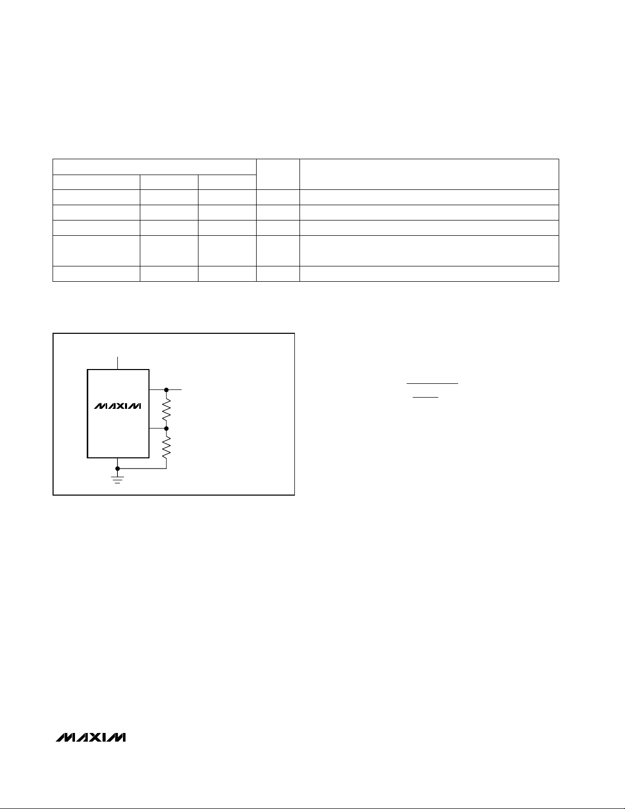
Setting the MAX6160 Output Voltage
Set the output voltage on the MAX6160 by connecting
a resistor divider between OUT, ADJ, and GND
(Figure 1). Choose R1 according to the following equation:
R1 = (1.06 x 10⁵) (V
OUT
/ V
ADJ
) Ω
where VTH= 1.23V. The scaling factor (1.06 x 10⁵)
compensates for the MAX6160's change in ADJ input
current over temperature. When R1 is chosen correctly,
the change in voltage across R1 caused by the ADJ
input current is properly cancelled. Choose R1 to within
±5% of this calculated value (nearest standard value
plus specified resistor tolerance) to optimize the output
voltage temperature coefficient. Using R1 = 215kΩ:
which is also the nearest 0.1% resistor value.
Choose R2 according to the following equation:
R2 = R1 / (V
OUT
/ V
ADJ
- 1)
For example, a 2.5V output requires R1 = (1.06 x 10⁵)
(2.5V / 1.23V) ≈ 215kΩ, which is the nearest standardvalue 0.1% resistor.
Input Bypassing
For the best line-transient performance, decouple the
input with a 0.1µF ceramic capacitor, as shown in the
Typical Operating Circuit. Locate the capacitor as
close to the device pin as possible. Where transient
performance is less important, no capacitor is
necessary.
Output Bypassing
The MAX6125/MAX6141/MAX6145/MAX6150/MAX6160
do not require an output capacitor. They are stable for
capacitive loads from 0nF to 10nF. If your application
requires an output charge reservoir (e.g., to decouple
the reference from a DAC’s input), then make sure that
the total output capacitive load does not exceed 10nF
for optimum settling-time performance.
MAX6125/MAX6141/MAX6145/MAX6150/MAX6160
SOT23, Low-Cost, Low-Dropout,
3-Terminal Voltage References
______________________________________________________________Pin Description
Adjustable output voltage feedback input. Connect a resistor
divider between OUT, ADJ, and GND (Figure 1).
ADJ5**
Input VoltageIN8
GroundGND4
No Connection. Not internally connected.N.C.2, 3, 5*, 6, 7
Reference OutputOUT1
FUNCTIONNAME
SO
—
1
3
—
2
SOT23-3
2
3
1
—
4
SOT143
*Except MAX6160.
**MAX6160 only.
Figure 1. MAX6160 Adjustable Output Circuit
PIN
V
IN
MAX6160
GND
IN
OUT
ADJ
V
OUT
R1
R2
V
OUT
ADJ
OUT
V
ADJ
R1
)
R1 = 1.06 x 10⁵ (––––) Ω
R2 = –—––––
V
–––– - 1
(
V
V
= 1.23V
ADJ
R2 =
215k
2.5V
1.23V
Ω
208k
≈Ω
-1

MAX6125/MAX6141/MAX6145/MAX6150/MAX6160
SOT23, Low-Cost, Low-Dropout,
3-Terminal Voltage References
8 _______________________________________________________________________________________
Ordering Information (continued)
PART
MAX6145ESA
MAX6145EUR-T -40°C to +85°C
-40°C to +85°C 8 SO
3 SOT23-3
TEMP
RANGE
PINPACKAGE
—
EDAA
TOP
MARK
MAX6160EUS-T -40°C to +85°C 4 SOT143-4 JXAA
MAX6150ESA
MAX6150EUR-T -40°C to +85°C
-40°C to +85°C 8 SO
3 SOT23-3
—
EEAA
MAX6160ESA
-40°C to +85°C 8 SO —
Chip Information
TRANSISTOR COUNT: 42
Typical Operating Circuit
V
= (V
IN
0.1µF*
*OPTIONAL
+ 200mV) to 12.6V
OUT
IN
MAX6125
MAX6141
MAX6145
MAX6150
GND
OUT
V
OUT

MAX6125/MAX6141/MAX6145/MAX6150/MAX6160
SOT23, Low-Cost, Low-Dropout,
3-Terminal Voltage References
Maxim cannot assume responsibility for use of any circuitry other than circuitry entirely embodied in a Maxim product. No circuit patent licenses are
implied. Maxim reserves the right to change the circuitry and specifications without notice at any time.
Maxim Integrated Products, 120 San Gabriel Drive, Sunnyvale, CA 94086 408-737-7600 _____________________ 9
© 2002 Maxim Integrated Products Printed USA is a registered trademark of Maxim Integrated Products.
Package Information
(The package drawing(s) in this data sheet may not reflect the most current specifications. For the latest package outline information
go to www.maxim-ic.com/packages.)
SOT23 L.EPS
 Loading...