

Page 1
General Description
The MAX6143 is a low-noise, high-precision voltage reference. The device features a proprietary temperaturecoefficient curvature-correction circuit and
laser-trimmed thin-film resistors that result in a very low
3ppm/°C temperature coefficient and excellent ±0.06%
initial accuracy. The MAX6143 provides a TEMP output
where the output voltage is proportional to die temperature, making the device suitable for a wide variety of
temperature-sensing applications. The device also provides a TRIM input, allowing fine trimming of the output
voltage with a resistive-divider network. Low temperature drift and low noise make the MAX6143 ideal for use
with high-resolution A/D or D/A converters.
The MAX6143 provides accurate preset +2.5V, +3.3V,
+4.096V, +5.0V, and +10V reference voltages and
accepts input voltages up to +40V. The device draws
340µA of supply current and sources 30mA or sinks 2mA
of load current. The active-low shutdown feature (SHDN)
reduces supply current to 0.01µA. The MAX6143 uses
bandgap technology for low-noise performance and
excellent accuracy. The MAX6143 does not require an
output bypass capacitor for stability, and is stable with
capacitive loads up to 100µF. Eliminating the output
bypass capacitor saves valuable board area in spacecritical applications.
The MAX6143 is available in an 8-pin SO package and
operates over the automotive (-40°C to +125°C) temperature range.
Applications
A/D Converters Voltage Regulators
D/A Converters Threshold Detectors
Digital Voltmeters
Features
♦ Wide (V
OUT
+ 2V) to +40V Supply Voltage Range
♦ Excellent Temperature Stability: 3ppm/°C (max)
♦ Tight Initial Accuracy: 0.05% (max)
♦ Low Noise: 3.8µV
P-P
(typ at 2.5V Output)
♦ Sources up to 30mA Output Current
♦ Low Supply Current: 450µA (max at +25°C)
♦ Low 0.01µA Shutdown Current
♦ Linear Temperature Transducer Voltage Output
♦ +2.5V, +3.3V, +4.096V, +5.0V, or +10V Output
Voltages
♦ Wide Operating Temperature Range: -40°C to
+125°C
♦ No External Capacitors Required for Stability
MAX6143
High-Precision Voltage Reference with
Temperature Sensor
________________________________________________________________ Maxim Integrated Products 1
19-3168; Rev 1; 4/04
For pricing, delivery, and ordering information, please contact Maxim/Dallas Direct! at
1-888-629-4642, or visit Maxim’s website at www.maxim-ic.com.
Pin Configuration appears at end of data sheet.
Ordering Information/Selector Guide
PART TEMP RANGE
PIN-
OUTPUT
TEMPERATURE COEFFICIENT
(ppm/°C) 40°C TO +125°C
INITIAL
ACCURACY (%)
MAX6143AASA25
8 SO 2.500 3 0.06
MAX6143BASA25
8 SO 2.500 10 0.10
MAX6143AASA33
8 SO 3.300 3 0.06
MAX6143BASA33
8 SO 3.300 10 0.10
MAX6143AASA41
8 SO 4.096 3 0.06
MAX6143BASA41
8 SO 4.096 10 0.10
MAX6143AASA50
8 SO 5.000 3 0.06
MAX6143BASA50
8 SO 5.000 10 0.10
MAX6143AASA10
8 SO 10.000 3 0.05
MAX6143BASA10
8 SO 10.000 10 0.10
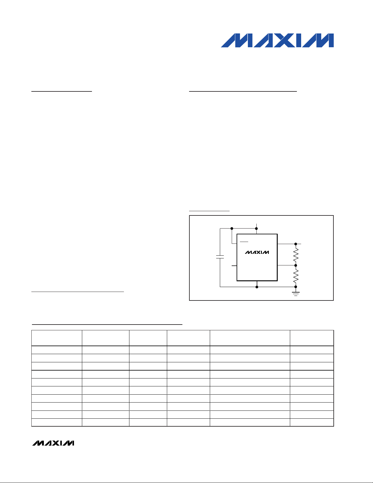
IN
OUT
GND
*OPTIONAL.
*
*
*
( V
OUT
+ 2V) TO 40V INPUT
REFERENCE
OUTPUT
SHDN
TRIM
TEMP
MAX6143
Typical Operating Circuit
PACKAGE
-40°C to +125°C
-40°C to +125°C
-40°C to +125°C
-40°C to +125°C
-40°C to +125°C
-40°C to +125°C
-40°C to +125°C
-40°C to +125°C
-40°C to +125°C
-40°C to +125°C
VOLTAGE (V)
Page 2
MAX6143
High-Precision Voltage Reference with
Temperature Sensor
2 _______________________________________________________________________________________
ABSOLUTE MAXIMUM RATINGS
Stresses beyond those listed under “Absolute Maximum Ratings” may cause permanent damage to the device. These are stress ratings only, and functional
operation of the device at these or any other conditions beyond those indicated in the operational sections of the specifications is not implied. Exposure to
absolute maximum rating conditions for extended periods may affect device reliability.
IN to GND...............................................................-0.3V to +42V
OUT, SHDN, TRIM, TEMP to GND...............-0.3V to (V
IN
+ 0.3V)
Output Short Circuit to GND.....................................................5s
Continuous Power Dissipation (T
A
= +70°C)
8-Pin SO (derate 5.9mW/°C above +70°C) ..................471mW
Operating Temperature Range ........................-40°C to +125°C
Junction Temperature .....................................................+150°C
Storage Temperature Range ............................-65°C to +150°C
Lead Temperature (soldering, 10s) ................................+300°C
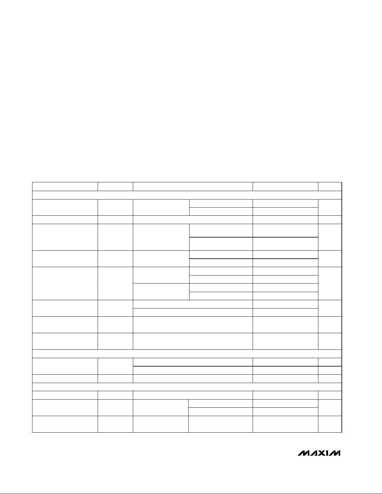
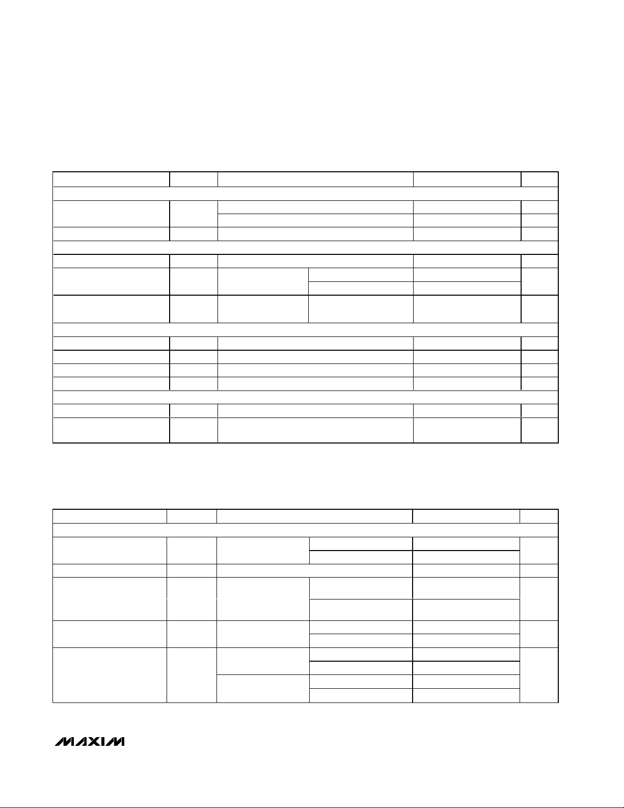
ELECTRICAL CHARACTERISTICS—MAX6143_25 (V
OUT
= 2.5V)
(VIN= V
SHDN
= +5V, TA= -40°C to +125°C, unless otherwise noted. Typical values are at TA= +25°C.) (Note 1)
PARAMETER
CONDITIONS
UNITS
OUTPUT
MAX6143A_25 (0.06%)
2.5
Output Voltage V
OUT
MAX6143B_25 (0.1%)
2.5
V
Output Adjustment Range
∆V
TRIM
R
POT
= 10kΩ±3 ±6%
MAX6143AASA 1.5 3Output-Voltage
Temperature Coefficient
(Note 2)
TCV
OUT
MAX6143BASA 3 10
ppm/°C
T
A
= +25°C 0.6 5
Line Regulation (Note 3)
4.5V ≤ VIN ≤ 40V
T
A
= -40°C to +125°C 0.8 10
ppm/V
T
A
= +25°C210
Sourcing:
0 ≤ I
OUT
≤ 10mA
T
A
= -40°C to +125°C215
T
A
= +25°C50
Load Regulation (Note 3)
∆V
OUT
/
∆I
OUT
Sinking:
-0.6mA ≤ I
OUT
≤ 0
T
A
= -40°C to +125°C90
ppm/mA
OUT shorted to GND 60
Output Short-Circuit
Current
I
SC
OUT shorted to IN 3
mA
Temperature Hysteresis
(Note 4)
∆V
OUT
/
cycle
ppm
Long-Term Stability
∆V
OUT
/
time
1000 hours at T
A
= +25°C50ppm
DYNAMIC
f = 0.1Hz to 10Hz 3.8
µV
P-P
Noise Voltage e
OUT
f = 10Hz to 1kHz 6.8
µV
RMS
Turn-On Settling Time t
R
To V
OUT
= 0.1% of final value, C
OUT
= 50pF
µs
INPUT
Supply Voltage Range V
IN
Guaranteed by line regulation test 4.5
V
TA = +25°C
Quiescent Supply Current
I
I
N
No load, normal
operation
T
A
= -40°C to +125°C
µA
Shutdown Supply Current
I
SHDN
No load, V
SHDN
<
0.8V
T
A
= -40°C to +125°C
5µA
SYMBOL
No load, TA = +25°C
TA = -40°C to +125°C
∆V
/ ∆V
OUT
IN
MIN TYP MAX
2.4985
2.4975
120
150
300 450
0.01
2.5015
2.5025
500
900
40.0
600
Page 3
MAX6143
High-Precision Voltage Reference with
Temperature Sensor
_______________________________________________________________________________________ 3
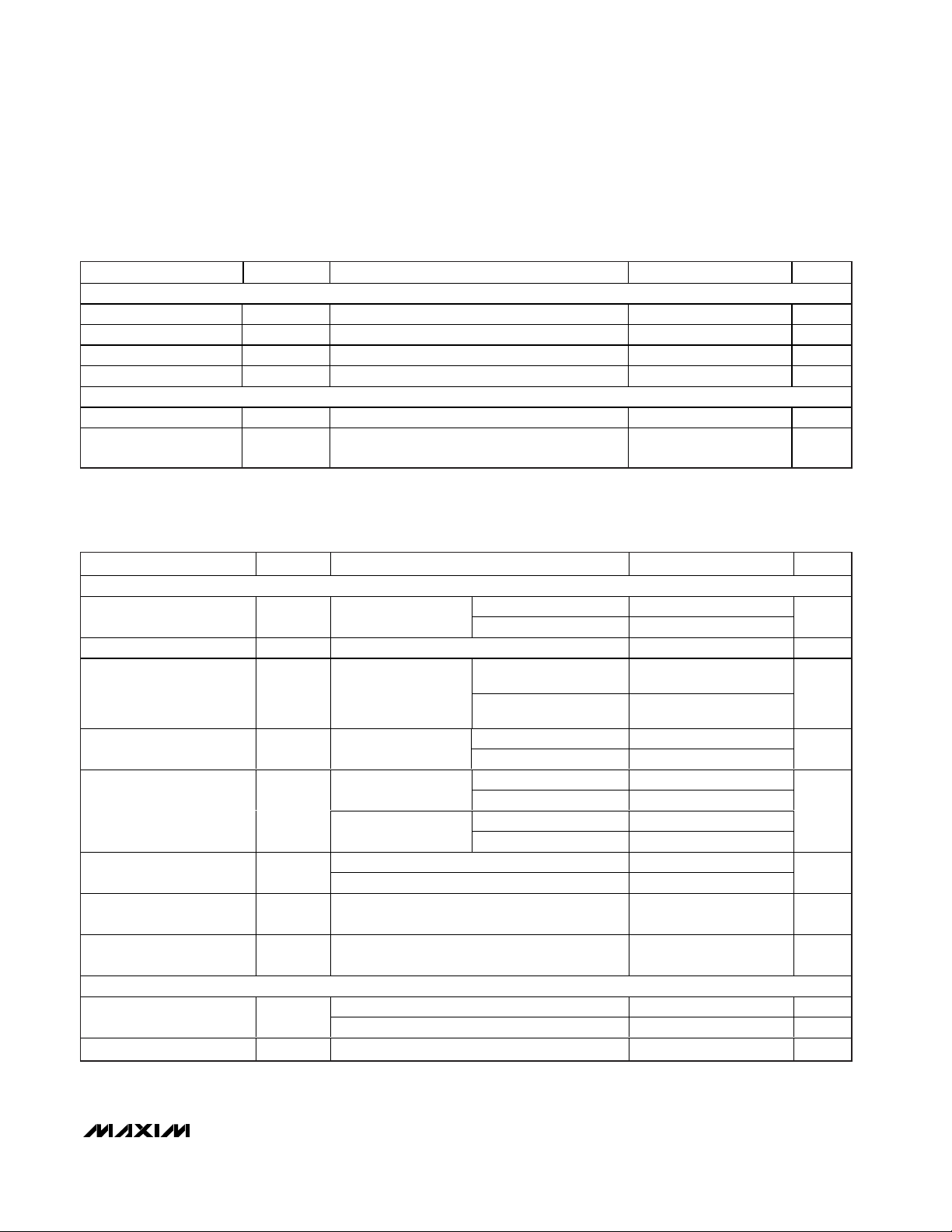
ELECTRICAL CHARACTERISTICS—MAX6143_33 (V
OUT
= 3.3V)
(VIN= V
SHDN
= +10V, TA= -40°C to +125°C, unless otherwise noted. Typical values are at TA= +25°C.) (Note 1)
PARAMETER
CONDITIONS
UNITS
OUTPUT
MAX6143A_33 (0.06%)
3.3
Output Voltage V
OUT
MAX6143B_33 (0.1%)
3.3
V
Output Adjustment Range ∆V
TRIMRPOT
= 10kΩ ±3 ±6%
MAX6143AASA 1.5 3
Output-Voltage
Temperature Coefficient
(Note 2)
MAX6143BASA 3 10
ppm/°C
TA = +25°C 0.6 5
Line Regulation (Note 3)
∆V
OUT
/
∆V
IN
5.3V ≤ VIN ≤ 40V
T
A
= -40°C to +125°C 0.8 10
ppm/V
TA = +25°C210
Sourcing:
0 ≤ I
OUT
≤ 10mA
T
A
= -40°C to +125°C215
TA = +25°C50
Load Regulation (Note 3)
∆V
OUT
/
∆I
OUT
Sinking:
-0.6mA ≤ I
OUT
≤ 0
T
A
= -40°C to +125°C90
ppm/
mA
OUT shorted to GND 60
Output Short-Circuit Current
I
SC
OUT shorted to IN 3
mA
Temperature Hysteresis
(Note 4)
∆V
OUT
/
cycle
ppm
Long-Term Stability
∆V
OUT
/
time
1000 hours at T
A
= +25°C50
ppm
DYNAMIC
f = 0.1Hz to 10Hz 5
µV
P-P
Noise Voltage e
OUT
f = 10Hz to 1kHz 9.3
µV
RMS
Turn-On Settling Time t
R
To V
OUT
= 0.1% of final value, C
OUT
= 50pF 180 µs
ELECTRICAL CHARACTERISTICS—MAX6143_25 (V
OUT
= 2.5V) (continued)
(VIN= V
SHDN
= +5V, TA= -40°C to +125°C, unless otherwise noted. Typical values are at TA= +25°C.) (Note 1)
PARAMETER
SYMBOL
CONDITIONS
MIN
TYP
MAX
UNITS
SHUTDOWN (SHDN)
Logic-High Input Voltage
V
IH
2.0 V
Logic-Low Input Voltage V
IL
0.8 V
Logic-High Input Current
I
IH
20 µA
Logic-Low Input Current I
IL
2µA
TEMP OUTPUT
TEMP Output Voltage V
TEMP
mV
TEMP Temperature
Coefficient
TC
TEMP
1.9
mV/°C
SYMBOL
No load, TA = +25°C
570
MIN TYP MAX
3.2980
3.2967
3.3020
3.3033
TCV
OUTTA
= -40°C to +125°C
500
900
120
Page 4
MAX6143
High-Precision Voltage Reference with
Temperature Sensor
4 _______________________________________________________________________________________
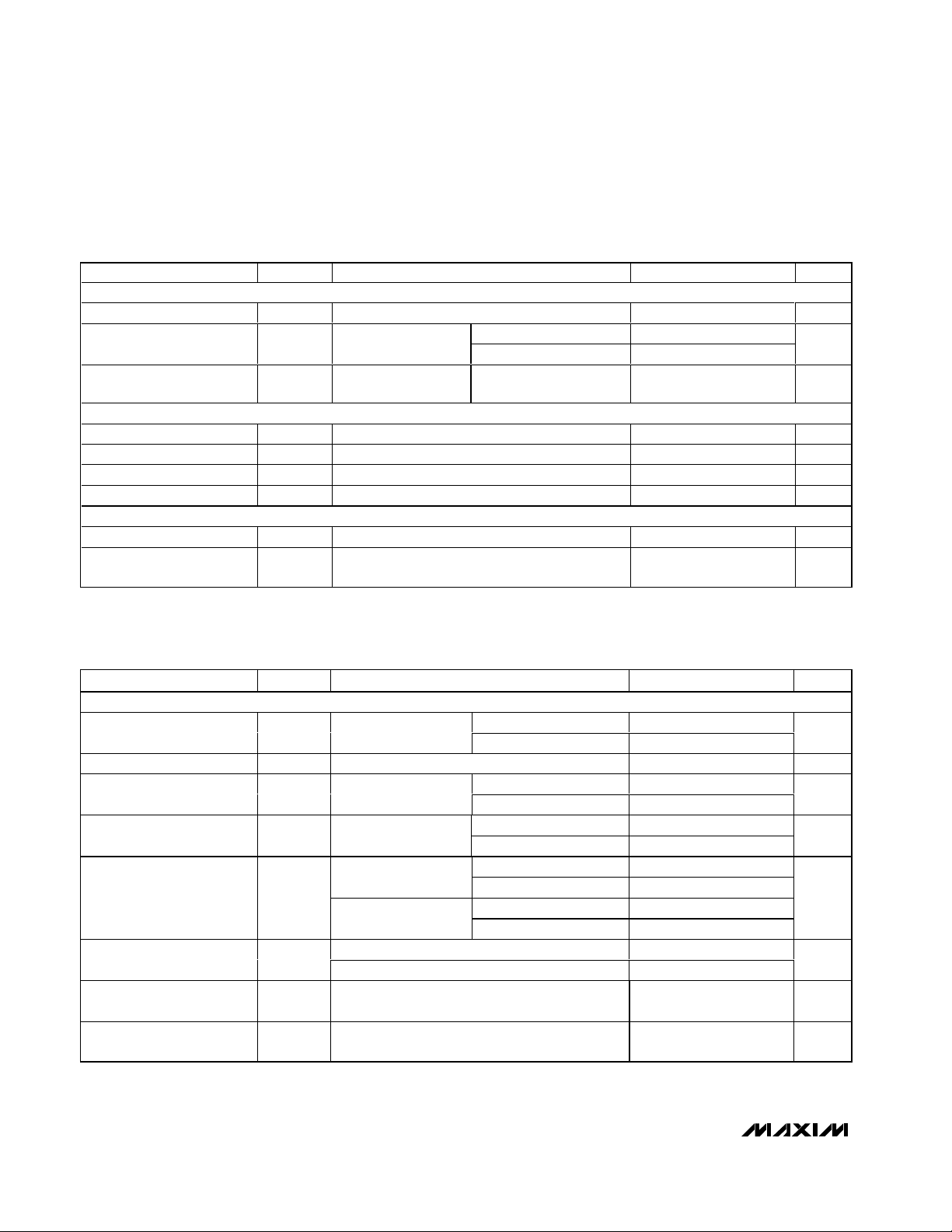
ELECTRICAL CHARACTERISTICS—MAX6143_41 (V
OUT
= 4.096V)
(VIN= V
SHDN
= +10V, TA= -40°C to +125°C, unless otherwise noted. Typical values are at TA= +25°C.) (Note 1)
PARAMETER
CONDITIONS
UNITS
OUTPUT
MAX6143A_41 (0.06%)
Output Voltage V
OUT
MAX6143B_41 (0.1%)
V
Output Adjustment Range
R
POT
= 10kΩ ±3 ±6%
MAX6143AASA 1.5 3
Output-Voltage Temperature
Coefficient (Note 2)
MAX6143BASA 3 10
ppm/°C
TA = +25°C 0.6 5
Line Regulation (Note 3)
∆V
OUT
/
∆V
IN
6.1V ≤ VIN ≤ 40V
T
A
= -40°C to +125°C 0.8 10
ppm/V
TA = +25°C210
Sourcing:
0 ≤ I
OUT
≤ 10mA
T
A
= -40°C to +125°C215
TA = +25°C50500
Load Regulation (Note 3)
∆V
OUT
/
∆I
OUT
Sinking:
-0.6mA ≤ I
OUT
≤ 0
T
A
= -40°C to +125°C90900
ppm/mA
OUT shorted to GND 60
Output Short-Circuit Current
I
SC
OUT shorted to IN 3
mA
Temperature Hysteresis
(Note 4)
∆V
OUT
/
cycle
ppm
Long-Term Stability
∆V
OUT
/
time
1000 hours at T
A
= +25°C50ppm
ELECTRICAL CHARACTERISTICS—MAX6143_33 (V
OUT
= 3.3V) (continued)
(VIN= V
SHDN
= +10V, TA= -40°C to +125°C, unless otherwise noted. Typical values are at TA= +25°C.) (Note 1)
PARAMETER
SYMBOL
CONDITIONS
MIN
TYP
MAX
UNITS
INPUT
Supply Voltage Range V
IN
Guaranteed by line regulation test 5.3
V
TA = +25°C 320
Quiescent Supply Current I
IN
No load, normal
operation
T
A
= -40°C to +125°C
µA
Shutdown Supply Current I
SHDN
No load, V
SHDN
<
0.8V
T
A
= -40°C to +125°C
5µA
SHUTDOWN (SHDN)
Logic-High Input Voltage V
IH
2.0 V
Logic-Low Input Voltage V
IL
0.8 V
Logic-High Input Current I
IH
20 µA
Logic-Low Input Current I
IL
2µA
TEMP OUTPUT
TEMP Output Voltage V
TEMP
630 mV
TEMP Temperature
Coefficient
2.1
mV/°C
TC
TEMP
SYMBOL
40.0
500
650
0.01
MIN TYP MAX
No load, TA = +25°C
∆V
TRIM
TCV
TA = -40°C to +125°C
OUT
4.0935 4.096 4.0985
4.0919 4.096 4.1001
120
Page 5
MAX6143
High-Precision Voltage Reference with
Temperature Sensor
_______________________________________________________________________________________ 5
ELECTRICAL CHARACTERISTICS—MAX6143_50 (V
OUT
= 5.0V)
(VIN= V
SHDN
= +15V, TA= -40°C to +125°C, unless otherwise noted. Typical values are at TA= +25°C.) (Note 1)
PARAMETER
SYMBOL
CONDITIONS
MIN
TYP
MAX
UNITS
OUTPUT
MAX6143A_50 (0.06%)
5.0
Output Voltage V
OUT
MAX6143B_50 (0.1%)
5.0
V
Output Adjustment Range ∆V
TRIM
R
POT
= 10kΩ ±3 ±6%
MAX6143AASA 1.5 3Output-Voltage
Temperature Coefficient
(Note 2)
MAX6143BASA 3 10
ppm/°C
TA = +25°C 0.6 5
Line Regulation (Note 3)
∆V
OUT
/
∆V
IN
7V ≤ VIN ≤ 40V
T
A
= -40°C to +125°C 0.8 10
ppm/V
TA = +25°C210
Sourcing:
0 ≤ I
OUT
≤ 10mA
T
A
= -40°C to +125°C215
TA = +25°C50
Load Regulation (Note 3)
∆V
OUT
/
∆I
OUT
Sinking:
-0.6mA ≤ I
OUT
≤ 0
T
A
= -40°C to +125°C90
ppm/mA
ELECTRICAL CHARACTERISTICS—MAX6143_41 (V
OUT
= 4.096V) (continued)
(VIN= V
SHDN
= +10V, TA= -40°C to +125°C, unless otherwise noted. Typical values are at TA= +25°C.) (Note 1)
PARAMETER
CONDITIONS
UNITS
DYNAMIC
f = 0.1Hz to 10Hz 7
µV
P-P
Noise Voltage e
OUT
f = 10Hz to 1kHz
µV
RMS
Turn-On Settling Time t
R
To V
OUT
= 0.1% of final value, C
OUT
= 50pF
µs
INPUT
Supply Voltage Range V
IN
Guaranteed by line regulation test 6.1
V
TA = +25°C
500
Quiescent Supply Current I
IN
No load, normal
operation
T
A
= -40°C to +125°C 650
µA
Shutdown Supply Current I
SHDN
No load, V
SHDN
<
0.8V
T
A
=-40°C to +125°C
5µA
SHUTDOWN (SHDN)
Logic-High Input Voltage V
IH
2.0 V
Logic-Low Input Voltage V
IL
0.8 V
Logic-High Input Current I
IH
20 µA
Logic-Low Input Current I
IL
2µA
TEMP OUTPUT
TEMP Output Voltage V
TEMP
mV
TEMP Temperature
Coefficient
(0.06%) 2.1
mV/°C
SYMBOL
TC
TEMP
MIN TYP MAX
11.5
200
40.0
320
0.01
630
No load, TA = +25°C
TCV
OUTTA
= -40°C to +125°C
4.9970
4.9950
5.0030
5.0050
500
900
Page 6

MAX6143
High-Precision Voltage Reference with
Temperature Sensor
6 _______________________________________________________________________________________
ELECTRICAL CHARACTERISTICS—MAX6143_50 (V
OUT
= 5.0V) (continued)
(VIN= V
SHDN
= +15V, TA= -40°C to +125°C, unless otherwise noted. Typical values are at TA= +25°C.) (Note 1)
PARAMETER
CONDITIONS
UNITS
OUT shorted to GND 60
Output Short-Circuit Current
I
SC
OUT shorted to IN 3
mA
Temperature Hysteresis
(Note 4)
∆V
OUT
/
cycle
ppm
Long-Term Stability
∆V
OUT
/
time
1000 hours at T
A
= +25°C50ppm
DYNAMIC
f = 0.1Hz to 10Hz 9
µV
P-P
Noise Voltage e
OUT
f = 10Hz to 1kHz
µV
RMS
Turn-On Settling Time t
R
To V
OUT
= 0.1% of final value, C
OUT
= 50pF
µs
INPUT
Supply Voltage Range V
IN
Guaranteed by line regulation test 7 40 V
TA = +25°C
Quiescent Supply Current I
IN
No load, normal
operation
T
A
= -40°C to +125°C
µA
Shutdown Supply Current I
SHDN
No load, V
SHDN
<
0.8V
T
A
= -40°C to +125°C
5µA
SHUTDOWN (SHDN)
Logic-High Input Voltage V
IH
2.0 V
Logic-Low Input Voltage V
IL
0.8 V
Logic-High Input Current I
IH
20 µA
Logic-Low Input Current I
IL
2µA
TEMP OUTPUT
TEMP Output Voltage V
TEMP
mV
TEMP Temperature
Coefficient
2.1
mV/°C
ELECTRICAL CHARACTERISTICS—MAX6143_10 (V
OUT
= 10V)
(VIN= V
SHDN
= +15V, TA= -40°C to +125°C, unless otherwise noted. Typical values are at TA= +25°C.) (Note 1)
PARAMETER
SYMBOL
CONDITIONS
MIN
TYP
MAX
UNITS
OUTPUT
MAX6143A_10 (0.05%)
Output Voltage V
OUT
MAX6143B_10 (0.1%)
V
Output Adjustment Range
∆V
TRIM
R
POT
= 10kΩ ±3 ±6%
MAX6143AASA 1.5 3Output-Voltage
Temperature Coefficient
(Note 2)
TCV
OUT
MAX6143BASA 3 10
p p m /° C
TA = +25°C 0.6 5
Line Regulation (Note 3)
∆V
OUT
/
∆V
IN
12V ≤ VIN ≤ 40V
T
A
= -40°C to +125°C 0.8 10
ppm/V
SYMBOL
MIN TYP MAX
120
14.5
230
320 550
700
0.01
TC
TEMP
No load, TA = +25°C
TA = -40°C to +125°C
9.995 10.0 10.005
9.990 10.0 10.010
630
Page 7

MAX6143
High-Precision Voltage Reference with
Temperature Sensor
_______________________________________________________________________________________ 7
ELECTRICAL CHARACTERISTICS—MAX6143_10 (V
OUT
= 10V) (continued)
(VIN= V
SHDN
= +15V, TA= -40°C to +125°C, unless otherwise noted. Typical values are at TA= +25°C.) (Note 1)
PARAMETER
SYMBOL
CONDITIONS
MIN
TYP
MAX
UNITS
TA = +25°C210
Sourcing:
0 ≤ I
OUT
≤ 10mA
T
A
= -40°C to +125°C215
TA = +25°C50500
Load Regulation (Note 3)
∆V
OUT
/
∆I
OUT
Sinking:
-0.6mA ≤ I
OUT
≤ 0
T
A
= -40°C to +125°C
90 900
p p m /m A
OUT shorted to GND 60
Output Short-Circuit
Current
I
SC
OUT shorted to IN 3
mA
Temperature Hysteresis
(Note 4)
∆V
OUT
/
cycle
ppm
Long-Term Stability
∆V
OUT
/
time
1000 hours at T
A
= +25°C50
ppm
DYNAMIC
f = 0.1Hz to 10Hz 18
µV
P-P
Noise Voltage e
OUT
f = 10Hz to 1kHz 29
µV
RMS
Turn-On Settling Time t
R
To V
OUT
= 0.1% of final value, C
OUT
= 50pF
µs
INPUT
Supply Voltage Range V
IN
Guaranteed by line regulation test 12 40 V
TA = +25°C
550
I
IN
No load, normal
operation
T
A
= -40°C to +125°C 700
µA
I
SHDN
No load, V
SHDN
<
0.8V
T
A
= -40°C to +125°C
5µA
SHUTDOWN (SHDN)
Logic-High Input Voltage V
IH
2.0 V
Logic-Low Input Voltage V
IL
0.8 V
Logic-High Input Current I
IH
20 µA
Logic-Low Input Current I
IL
2µA
TEMP OUTPUT
TEMP Output Voltage V
TEMP
mV
TEMP Temperature
Coefficient
TC
TEMP
2.1
mV/°C
Note 1: All devices are 100% production tested at TA= +25°C and guaranteed by design over TA= T
MIN
to T
MAX
, as specified.
Note 2: Temperature coefficient is defined as ∆V
OUT
divided by the temperature range.
Note 3: Line and load regulation specifications do not include the effects of self-heating.
Note 4: Thermal hysteresis is defined as the change in +25°C output voltage before and after cycling the device from T
MAX
to T
MIN
.
Quiescent Supply Current
Shutdown Supply Current
120
400
340
0.01
630
Page 8

MAX6143
High-Precision Voltage Reference with
Temperature Sensor
8 _______________________________________________________________________________________
2.498
2.500
2.499
2.501
2.502
OUTPUT VOLTAGE vs. TEMPERATURE
(V
OUT
= 2.5V)
MAX6143toc01
TEMPERATURE (°C)
OUTPUT VOLTAGE (V)
-50 25 50-25 0 75 100 125
THREE TYPICAL PARTS
9.993
9.998
9.995
10.001
9.999
9.996
10.002
9.997
9.994
10.000
10.003
OUTPUT VOLTAGE vs. TEMPERATURE
(V
OUT
= 10V)
MAX6143toc02
TEMPERATURE (°C)
OUTPUT VOLTAGE (V)
-50 25 50-25 0 75 100 125
THREE TYPICAL PARTS
0.50
0.25
0
-0.25
-0.50
015510 202530
LOAD REGULATION vs.
SOURCE CURRENT (V
OUT
= 2.5V)
MAX6143toc03
SOURCE CURRENT (mA)
OUTPUT VOLTAGE CHANGE (mV)
TA = -40°C
TA = +125°C
TA = +25°C
0.50
0.25
0
-0.25
-0.50
015510 202530
LOAD REGULATION
vs. SOURCE CURRENT (V
OUT
= 10V)
MAX6143toc04
SOURCE CURRENT (mA)
OUTPUT VOLTAGE CHANGE (mV)
TA = +25°C
TA = +125°C
TA = -40°C
1.00
0.75
0.50
0.25
-0.25
0
-0.50
0 1.00.5 1.5 2.0
LOAD REGULATION
vs. SINK CURRENT (V
OUT
= 2.5V)
MAX6143toc05
SINK CURRENT (mA)
OUTPUT VOLTAGE CHANGE (mV)
TA = +25°C
TA = +125°C
TA = -40°C
2.0
1.5
1.0
0.5
-0.5
0
-1.0
0 1.00.5 1.5 2.0
LOAD REGULATION
vs. SINK CURRENT (V
OUT
= 10V)
MAX6143toc06
SINK CURRENT (mA)
OUTPUT VOLTAGE CHANGE (mV)
TA = -40°C
TA = +125°C
TA = +25°C
0
60
20
40
80
100
LINE REGULATION vs. TEMPERATURE
(V
OUT
= 2.5V)
MAX6143toc07
INPUT VOLTAGE (V)
OUTPUT VOLTAGE CHANGE (µV)
0202551015 303540
TA = -40°C
TA = +125°C
TA = +25°C
0
150
50
100
200
250
300
LINE REGULATION vs. TEMPERATURE
(V
OUT
= 10V)
MAX6143toc08
INPUT VOLTAGE (V)
OUTPUT VOLTAGE CHANGE (µV)
12 28 3216 20 24 36 40
TA = -40°C
TA = +125°C
TA = +25°C
0.5
1.5
1.0
2.0
2.5
MINIMUM INPUT-OUTPUT DIFFERENTIAL
vs. SOURCE CURRENT (V
OUT
= 2.5V)
MAX6143toc09
SOURCE CURRENT (mA)
DROPOUT VOLTAGE (V)
0121648 20
TA = -40°C
TA = +125°C
TA = +25°C
Typical Operating Characteristics
(VIN= +5V for V
OUT
= +2.5V, VIN= +15V for V
OUT
= +10V, I
OUT
= 0, TA= +25°C, unless otherwise noted.)
Page 9

MAX6143
High-Precision Voltage Reference with
Temperature Sensor
_______________________________________________________________________________________ 9
0.5
1.5
1.0
2.0
2.5
MINIMUM INPUT-OUTPUT DIFFERENTIAL
vs. SOURCE CURRENT (V
OUT
= 10V)
MAX6143toc10
SOURCE CURRENT (mA)
DROPOUT VOLTAGE (V)
0121648 20
TA = -40°C
TA = +125°C
TA = +25°C
-140
-100
-120
-60
-80
-20
-40
0
0.001 0.1 10.01 10 100 1000
POWER-SUPPLY REJECTION RATIO
vs. FREQUENCY (V
OUT
= 2.5V)
MAX6143toc11
FREQUENCY (kHz)
PSRR (dB)
-120
-100
-60
-80
-20
-40
0
0.001 0.1 10.01 10 100 1000
POWER-SUPPLY REJECTION RATIO
vs. FREQUENCY (V
OUT
= 10V)
MAX6143toc12
FREQUENCY (kHz)
PSRR (dB)
0.001
0.1
0.01
10
1
100
0.1 10.01 10 100 1000
OUTPUT IMPEDANCE vs. FREQUENCY
(V
OUT
= 2.5V)
MAX6143toc13
FREQUENCY (kHz)
OUTPUT IMPEDANCE (Ω)
0
100
50
200
150
250
300
350
400
0101552025303540
SUPPLY CURRENT vs. INPUT VOLTAGE
(V
OUT
= 2.5V)
MAX6143toc14
INPUT VOLTAGE (V)
SUPPLY CURRENT (µA)
TA = -40°C
TA = +125°C
TA = +25°C
0
100
50
200
150
250
300
350
400
0101552025303540
SUPPLY CURRENT vs. INPUT VOLTAGE
(V
OUT
= 10V)
MAX6143toc15
INPUT VOLTAGE (V)
SUPPLY CURRENT (µA)
TA = -40°C
TA = +125°C
TA = +25°C
250
300
275
325
350
-50 -25 0 25 50 75 100 125
SUPPLY CURRENT vs. TEMPERATURE
(V
OUT
= 2.5V)
MAX6143toc16
TEMPERATURE (°C)
SUPPLY CURRENT (µA)
250
325
300
275
350
375
-50 -25 0 25 50 75 100 125
SUPPLY CURRENT vs. TEMPERATURE
(V
OUT
= 10V)
MAX6143toc17
TEMPERATURE (°C)
SUPPLY CURRENT (µA)
0.01
1
0.1
10
100
-50 -25 0 25 50 75 100 125
SHUTDOWN SUPPLY CURRENT
vs. TEMPERATURE (V
OUT
= 2.5V)
MAX6143toc18
TEMPERATURE (°C)
SHUTDOWN CURRENT (nA)
Typical Operating Characteristics (continued)
(VIN= +5V for V
OUT
= +2.5V, VIN= +15V for V
OUT
= +10V, I
OUT
= 0, TA= +25°C, unless otherwise noted.)
Page 10

MAX6143
High-Precision Voltage Reference with
Temperature Sensor
10 ______________________________________________________________________________________
Typical Operating Characteristics (continued)
(VIN= +5V for V
OUT
= +2.5V, VIN= +15V for V
OUT
= +10V, I
OUT
= 0, TA= +25°C, unless otherwise noted.)
0.01
1
0.1
10
100
-50 -25 0 25 50 75 100 125
SHUTDOWN SUPPLY CURRENT
vs. TEMPERATURE (V
OUT
= 10V)
MAX6143toc19
TEMPERATURE (°C)
SHUTDOWN CURRENT (nA)
400
600
500
700
800
-50 -25 0 25 50 75 100 125
TEMP VOLTAGE
vs. TEMPERATURE (V
OUT
= 2.5V)
MAX6143toc20
TEMPERATURE (°C)
TEMP VOLTAGE (mV)
400
600
500
800
700
900
-50 -25 0 25 50 75 100 125
TEMP VOLTAGE
vs. TEMPERATURE (V
OUT
= 10V)
MAX6143toc21
TEMPERATURE (°C)
TEMP VOLTAGE (mV)
2.35
2.50
2.45
2.40
2.60
2.55
2.65
0 0.5 1.0 1.5 2.0 2.5
OUTPUT VOLTAGE
vs. TRIM VOLTAGE (V
OUT
= 2.5V)
MAX6143toc22
TRIM VOLTAGE (V)
OUTPUT VOLTAGE (V)
2.498
2.500
2.499
2.501
2.502
0 200 400 600 800 1000
LONG-TERM STABILITY vs. TIME
(V
OUT
= 2.500V)
MAX6143toc23
TIME (hours)
V
OUT
(V)
TWO TYPICAL PARTS
9.998
10.000
9.999
10.001
10.002
0 200 400 600 800 1000
LONG-TERM STABILITY vs. TIME
(V
OUT
= 10.0V)
MAX6143toc24
TIME (hours)
V
OUT
(V)
TWO TYPICAL PARTS
1000
100
OUTPUT VOLTAGE-NOISE DENSITY
vs. FREQUENCY (V
OUT
= 2.5V)
MAX6143toc25
FREQUENCY (Hz)
OUTPUT VOLTAGE-NOISE DENSITY (nV/√Hz)
0.1 100 1000110
10,000
1000
100
OUTPUT VOLTAGE-NOISE DENSITY
vs. FREQUENCY (V
OUT
= 10V)
MAX6143toc26
FREQUENCY (Hz)
OUTPUT VOLTAGE-NOISE DENSITY (nV/√Hz)
0.1 100 1000110
0.1Hz TO 10Hz OUTPUT NOISE
MAX6143toc27
1µV/div
1s/div
Page 11

MAX6143
High-Precision Voltage Reference with
Temperature Sensor
______________________________________________________________________________________ 11
0.1Hz TO 10Hz OUTPUT NOISE
MAX6143toc28
4µV/div
1s/div
LOAD TRANSIENT
(V
OUT
= 2.5V, C
OUT
= 0, 0 TO 20mA)
MAX6413toc29
I
OUT
V
OUT
AC-COUPLED
1V/div
0
20mA
10µs/div
LOAD TRANSIENT
(V
OUT
= 10V, C
OUT
= 0, 0 TO 20mA)
MAX6413toc30
I
OUT
V
OUT
AC-COUPLED
1V/div
0
20mA
10µs/div
LOAD TRANSIENT
(V
OUT
= 2.5V, C
OUT
= 1µF, 0 TO +20mA)
MAX6413toc31
I
OUT
V
OUT
AC-COUPLED
50mV/div
0
20mA
200µs/div
LOAD TRANSIENT
(V
OUT
= 10V, C
OUT
= 1µF, 0 TO 20mA)
MAX6413toc32
I
OUT
V
OUT
AC-COUPLED
100mV/div
0
20mA
100µs/div
LOAD TRANSIENT
(V
OUT
= 2.5V, C
OUT
= 0, 0 TO -2mA)
MAX6413toc33
I
OUT
V
OUT
AC-COUPLED
200mV/div
0
-2mA
40µs/div
LOAD TRANSIENT
(V
OUT
= 10V, C
OUT
= 0, 0 TO -2mA)
MAX6413toc34
I
OUT
V
OUT
AC-COUPLED
20mV/div
0
-2mA
200µs/div
LOAD TRANSIENT
(V
OUT
= 2.5V, C
OUT
= 1µF, 0 TO -2mA)
MAX6413toc35
I
OUT
V
OUT
AC-COUPLED
20mV/div
0
-2mA
400µs/div
LOAD TRANSIENT
(V
OUT
= 10V, C
OUT
= 1µF, 0 TO -2mA)
MAX6413toc36
I
OUT
V
OUT
AC-COUPLED
5mV/div
0
-2mA
400µs/div
Typical Operating Characteristics (continued)
(VIN= +5V for V
OUT
= +2.5V, VIN= +15V for V
OUT
= +10V, I
OUT
= 0, TA= +25°C, unless otherwise noted.)
Page 12

MAX6143
High-Precision Voltage Reference with
Temperature Sensor
12 ______________________________________________________________________________________
Typical Operating Characteristics (continued)
(VIN= +5V for V
OUT
= +2.5V, VIN= +15V for V
OUT
= +10V, I
OUT
= 0, TA= +25°C, unless otherwise noted.)
LINE TRANSIENT
(V
OUT
= 2.5V)
MAX6413toc37
V
IN
V
OUT
AC-COUPLED
200mV/div
5.5V
4.5V
10µs/div
C
OUT
= 0
LINE TRANSIENT
(V
OUT
= 10V)
MAX6413toc38
V
IN
1V/div
V
OUT
AC-COUPLED
200mV/div
15.5V
14.5V
2µs/div
TURN-ON TRANSIENT
(V
OUT
= 2.5V, C
OUT
= 0)
MAX6413toc39
V
IN
2V/div
V
OUT
1V/div
GND
GND
10µs/div
C
OUT
= 0
TURN-ON TRANSIENT
(V
OUT
= 2.5V, C
OUT
= 1µF)
MAX6413toc40
V
IN
2V/div
V
OUT
1V/div
GND
GND
40µs/div
TURN-ON TRANSIENT
(V
OUT
= 10V, C
OUT
= 0)
MAX6413toc41
V
IN
5V/div
V
OUT
5V/div
GND
GND
100µs/div
TURN-ON TRANSIENT
(V
OUT
= 10V, C
OUT
= 1µF)
MAX6413toc42
V
IN
5V/div
V
OUT
5V/div
GND
GND
200µs/div
SHUTDOWN TRANSIENT
(V
OUT
= 2.5V, VIN = 5V, C
OUT
= 0)
MAX6413toc43
V
SHDN
2V/div
V
OUT
1V/div
GND
GND
10µs/div
SHUTDOWN TRANSIENT
(V
OUT
= 2.5V, VIN = 5V, C
OUT
= 1µF)
MAX6413toc44
V
SHDN
2V/div
+5V
V
OUT
1V/div
GND
GND
40µs/div
Page 13

Detailed Description
The MAX6143 precision voltage reference provides
accurate preset +2.5V, +3.3V, +4.096V, +5.0V, and
+10V reference voltages from up to +40V input voltages.
These devices feature a proprietary temperature-coefficient curvature-correction circuit and laser-trimmed thinfilm resistors that result in a very low 3ppm/°C
temperature coefficient and excellent 0.05% initial accuracy. The MAX6143 draws 340µA of supply current and
sources 30mA or sinks 2mA of load current.
Trimming the Output Voltage
Trim the factory-preset output voltage on the MAX6143
by placing a resistive-divider network between OUT,
TRIM, and GND. Use the following formula to calculate
the change in output voltage from its preset value:
∆V
OUT
= 2 x (V
TRIM
- V
TRIM (open)
) x k
where:
V
TRIM
= 0 to V
OUT
V
TRIM
(open)
= V
OUT
(nominal) / 2 (typ)
k = ±6% typ
For example, use a 50kΩ potentiometer (such as the
MAX5436) between OUT, TRIM, and GND with the
potentiometer wiper connected to TRIM (see Figure 2).
As the TRIM voltage changes from V
OUT
to GND, the
output voltage changes accordingly. Set R2 to 1MΩ or
less. Currents through resistors R1 and R2 add to the
quiescent supply current.
Typical Operating Characteristics (continued)
(VIN= +5V for V
OUT
= +2.5V, VIN= +15V for V
OUT
= +10V, I
OUT
= 0, TA= +25°C, unless otherwise noted.)
SHUTDOWN TRANSIENT
(V
OUT
= 10V, VIN = 15V, C
OUT
= 0)
MAX6413toc45
V
SHDN
5V/div
V
OUT
5V/div
GND
GND
100µs/div
SHUTDOWN TRANSIENT
(V
OUT
= 10V, VIN = 15V, C
OUT
= 1µF)
MAX6143toc46
V
SHDN
5V/div
V
OUT
5V/div
GND
GND
100µs/div
MAX6143
High-Precision Voltage Reference with
Temperature Sensor
______________________________________________________________________________________ 13
PIN NAME FUNCTION
1, 8 I.C. Internally Connected. Do not connect externally.
2INPositive Power-Supply Input
3 TEMP
Temperature Proportional Output Voltage. TEMP generates an output voltage proportional to the die
temperature.
4 GND Ground
5 TRIM
Output Voltage Trim. Connect TRIM to the center of a voltage-divider between OUT and GND for
trimming. Leave unconnected to use the preset output voltage.
6 OUT Output Voltage
7 SHDN Active-Low Shutdown. Connect SHDN to IN for normal operation.
Pin Description
Page 14

MAX6143
High-Precision Voltage Reference with
Temperature Sensor
14 ______________________________________________________________________________________
Temp Output
The MAX6143 provides a temperature output proportional to die temperature. TEMP can be calculated from
the following formula:
TEMP (V) = TJ(°K) x n
where TJ= the die temperature,
n = the temperature multiplier,
TA= the ambient temperature.
Self-heating affects the die temperature and converse-
ly, the TEMP output. The TEMP equation assumes the
output is not loaded. If device power dissipation is negligible, then TJ≈ TA.
Applications Information
Bypassing/Output Capacitance
For the best line-transient performance, decouple the
input with a 0.1µF ceramic capacitor as shown in the
Typical Operating Circuit. Place the capacitor as close
to IN as possible. When transient performance is less
important, no capacitor is necessary.
The MAX6143 does not require an output capacitor for
stability and is stable with capacitive loads up to 100µF.
In applications where the load or the supply can experience step changes, a larger output capacitor reduces
the amount of overshoot (undershoot) and improves the
circuit’s transient response. Place output capacitors as
close to the device as possible for best performance.
Supply Current
The MAX6143 consumes 340µA of quiescent supply
current. This improved efficiency reduces power dissipation and extends battery life.
Shutdown
The active-low shutdown feature reduces supply current to 0.01µA (typ), further extending battery life.
Connect SHDN to GND to activate shutdown. Connect
SHDN to IN for normal operation.
Thermal Hysteresis
Thermal hysteresis is the change in the output voltage
at TA= +25°C before and after the device is cycled
over its entire operating temperature range. Hysteresis
is caused by differential package stress appearing
across the bandgap core transistors. The typical thermal hysteresis value is 120ppm.
Turn-On Time
The MAX6143 typically turns on and settles to within
0.1% of the preset output voltage in 150µs (2.5V
output). The turn-on time can increase up to 150µs with
the device operating at a 1µF load.
Short-Circuited Outputs
The MAX6143 features a short-circuit-protected output.
Internal circuitry limits the output current to 60mA when
short circuiting the output to ground. The output current is limited to 3mA when short circuiting the output
to the input.
n
VatTT
T
mV K
TEMP J
( )
./=
=
≅ °
0
0
19
TEMPERATURE
COEFFICIENT
(ppm/°C)
110
100
16-BIT
14-BIT
12-BIT
10-BIT
8-BIT
0.01
0.1
10
100
1000
1
10,000
18-BIT
20-BIT
OPERATING TEMPERATURE RANGE (T
MAX
- T
MIN
) (°C)
Figure 1. Temperature Coefficient vs. Operating Temperature Range for a 1 LSB Maximum Error
Page 15

Temperature Coefficient vs. Operating
Temperature Range for a
1 LSB Maximum Error
In a data converter application, the reference voltage
of the converter must stay within a certain limit to keep
the error in the data converter smaller than the resolution limit through the operating temperature range.
Figure 1 shows the maximum allowable reference-voltage temperature coefficient to keep the conversion
error to less than 1 LSB, as a function of the operating
temperature range (T
MAX
- T
MIN
) with the converter
resolution as a parameter. The graph assumes the reference-voltage temperature coefficient as the only
parameter affecting accuracy.
In reality, the absolute static accuracy of a data converter is dependent on the combination of many parameters such as integral nonlinearity, differential
nonlinearity, offset error, gain error, as well as voltagereference changes.
MAX6143
High-Precision Voltage Reference with
Temperature Sensor
______________________________________________________________________________________ 15
IN
OUT
GND
*OPTIONAL.
*
( V
OUT
+ 2V) TO 40V INPUT
REFERENCE
OUTPUT
MAX5436
50kΩ
POTENTIOMETER
SHDN
TRIM
TEMP
MAX6143
Figure 2. Applications Circuit Using the MAX5436 Potrntiometer
Chip Information
TRANSISTOR COUNT: 429
PROCESS: BiCMOS
OUT
TRIMGND
*INTERNALLY CONNECTED. DO NOT CONNECT.
1
2
87I.C.*
SHDNIN
TEMP
I.C.*
SO
TOP VIEW
3
4
6
5
MAX6143
Pin Configuration
Page 16

MAX6143
High-Precision Voltage Reference with
Temperature Sensor
Maxim cannot assume responsibility for use of any circuitry other than circuitry entirely embodied in a Maxim product. No circuit patent licenses are
implied. Maxim reserves the right to change the circuitry and specifications without notice at any time.
16 ____________________Maxim Integrated Products, 120 San Gabriel Drive, Sunnyvale, CA 94086 408-737-7600
© 2004 Maxim Integrated Products Printed USA is a registered trademark of Maxim Integrated Products.
Package Information
(The package drawing(s) in this data sheet may not reflect the most current specifications. For the latest package outline information
go to www.maxim-ic.com/packages
.)
SOICN .EPS
PACKAGE OUTLINE, .150" SOIC
1
1
21-0041
B
REV.DOCUMENT CONTROL NO.APPROVAL
PROPRIETARY INFORMATION
TITLE:
TOP VIEW
FRONT VIEW
MAX
0.010
0.069
0.019
0.157
0.010
INCHES
0.150
0.007
E
C
DIM
0.014
0.004
B
A1
MIN
0.053A
0.19
3.80 4.00
0.25
MILLIMETERS
0.10
0.35
1.35
MIN
0.49
0.25
MAX
1.75
0.050
0.016L
0.40 1.27
0.3940.386D
D
MINDIM
D
INCHES
MAX
9.80 10.00
MILLIMETERS
MIN
MAX
16
AC
0.337 0.344 AB8.758.55 14
0.189 0.197 AA5.004.80 8
N MS012
N
SIDE VIEW
H 0.2440.228 5.80 6.20
e 0.050 BSC 1.27 BSC
C
HE
e
B
A1
A
D
0∞-8∞
L
1
VARIATIONS:
 Loading...