

Page 1
General Description
The MAX6138 is a precision, two-terminal shunt mode,
bandgap voltage reference available in fixed reverse
breakdown voltages of 1.2205V, 2.048V, 2.5V, 3.0V,
3.3V, 4.096V, and 5.0V. Ideal for space-critical applications, the MAX6138 is offered in the subminiature 3-pin
SC70 surface-mount package (1.8mm X 1.8mm), 50%
smaller than comparable devices in SOT23 surfacemount packages.
Laser-trimmed resistors ensure precise initial accuracy.
With a 25ppm/°C temperature coefficient, the device is
offered in three grades of initial accuracy ranging from
0.1% to 0.5%. The MAX6138 has a 60µA to 15mA shuntcurrent capability with low-dynamic impedance, ensuring
stable reverse breakdown voltage accuracy over a wide
range of operating temperatures and currents.
The MAX6138 does not require an external stabilizing
capacitor while ensuring stability with capacitive loads.
The MAX6138 is a higher precision device in a smaller
package than the LM4040/LM4050.
Applications
Portable, Battery-Powered Equipment
Notebook Computers
Cell Phones
Industrial Process Control
Features
♦ Ultra-Small 3-Pin SC70 Package
♦ 0.1% (max) Initial Accuracy
♦ 25ppm/°C (max) Temperature Coefficient
Guaranteed Over -40°C to +85°C Temperature
Range
♦ Wide Operating Current Range: 60µA to 15mA
♦ Low 28µV
RMS
Output Noise (10Hz to 10kHz)
♦ 1.2205V, 2.048V, 2.5V, 3.0V, 3.3V, 4.096V, and 5.0V
Fixed Reverse Breakdown Voltages
♦ No Output Capacitors Required
♦ Stable with Capacitive Loads
MAX6138
0.1%, 25ppm, SC70 Shunt Voltage Reference
with Multiple Reverse Breakdown Voltages
________________________________________________________________ Maxim Integrated Products 1
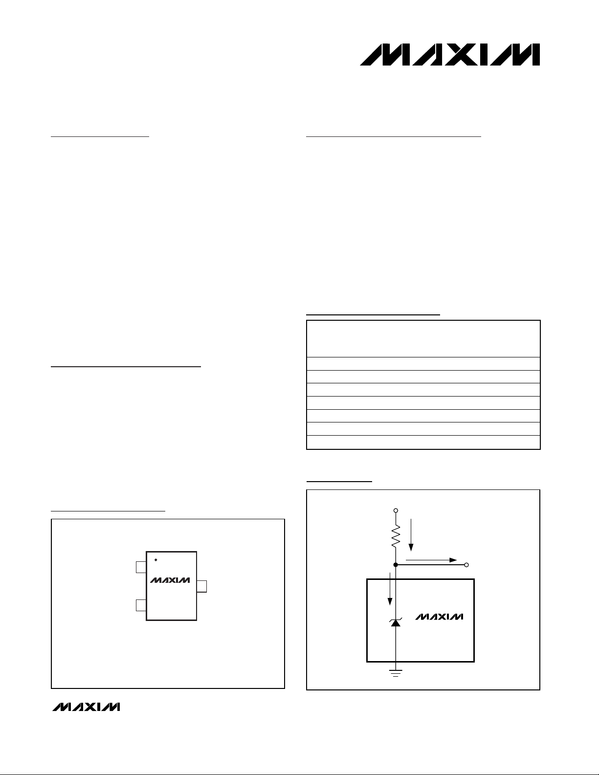
Pin Configuration
Selector Guide
Typical Operating Circuit
19-2090; Rev 2; 4/04
For pricing, delivery, and ordering information, please contact Maxim/Dallas Direct! at
1-888-629-4642, or visit Maxim’s website at www.maxim-ic.com.
Ordering Information appears at end of data sheet.
PART
MAX6138_EXR12-T -40°C to +85°C 3 SC70-3 1.2205
MAX6138_EXR21-T -40°C to +85°C 3 SC70-3 2.0480
MAX6138_EXR25-T -40°C to +85°C 3 SC70-3 2.5000
MAX6138_EXR30-T -40°C to +85°C 3 SC70-3 3.0000
MAX6138_EXR33-T -40°C to +85°C 3 SC70-3 3.3000
MAX6138_EXR41-T -40°C to +85°C 3 SC70-3 4.0960
MAX6138_EXR50-T -40°C to +85°C 3 SC70-3 5.0000
TEMP
RANGE
PINPACKAGE
OUTPUT
VOLTAGE
(V)
V
S
I
+ I
SHUNT
R
I
SHUNT
S
TOP VIEW
1
+
MAX6138
-
2
SC70
*PIN 3 MUST BE LEFT FLOATING
OR CONNECTED TO PIN 2.
3 N.C.*
LOAD
I
LOAD
MAX6138
V
R
Page 2
MAX6138
0.1%, 25ppm, SC70 Shunt Voltage Reference
with Multiple Reverse Breakdown Voltages
2 _______________________________________________________________________________________
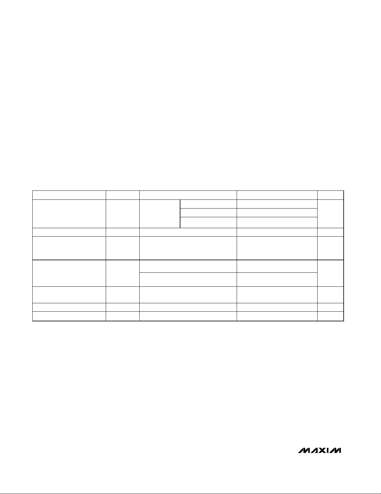
ABSOLUTE MAXIMUM RATINGS
ELECTRICAL CHARACTERISTICS—MAX6138_12 (1.2205V)
(IR= 100µA, TA= -40°C to +85°C, unless otherwise noted. Typical values are at TA= +25°C.) (Note 1)
Stresses beyond those listed under “Absolute Maximum Ratings” may cause permanent damage to the device. These are stress ratings only, and functional
operation of the device at these or any other conditions beyond those indicated in the operational sections of the specifications is not implied. Exposure to
absolute maximum rating conditions for extended periods may affect device reliability.
Reverse Current (cathode to anode) ..................................20mA
Forward Current (anode to cathode) ..................................10mA
Continuous Power Dissipation (T
A
A
= +70°C)
3-Pin SC70 (derate 2.17mW/°C above +70°C) ...........174mW
Operating Temperature Range .........................-40°C to +125°C
Storage Temperature Range .............................-65°C to +150°C
Junction Temperature......................................................+150°C
Lead Temperature (soldering, 10s) .................................+300°C
PARAMETER SYMBOL CONDITIONS MIN TYP MAX UNITS
Reverse Breakdown Voltage
(Note 2)
Minimum Operating Current I
Reverse Voltage
Temperature Coefficient
(Notes 2, 3)
V
R
RMIN
TC 4 25 ppm/°C
TA = +25°C
MAX6138A (0.1%) 1.2193 1.2205 1.2217
MAX6138B (0.2%) 1.2181 1.2205 1.2229
MAX6138C (0.5%) 1.2144 1.2205 1.2266
45 60 µA
V
Reverse Breakdown Voltage
Change with Operating
Current Change
Reverse Dynamic
Impedance (Note 3)
Wideband Noise e
Reverse Breakdown Voltage
∆V
∆V
I
≤ IR ≤ 1mA 0.3 1.0
RMIN
/∆I
R
R
1mA ≤ IR ≤ 12mA 2.5 8.0
Z
R
N
R
IR = 1mA, f = 120Hz, IAC = 0.1I
IR = 10µA, 10Hz ≤ f ≤ 10kHz 20 µV
t = 1000h
R
0.3 0.8 Ω
120 ppm
mV
RMS
Page 3
MAX6138
0.1%, 25ppm, SC70 Shunt Voltage Reference
with Multiple Reverse Breakdown Voltages
_______________________________________________________________________________________ 3
ELECTRICAL CHARACTERISTICS—MAX6138_21 (2.048V)
(IR= 100µA, TA= -40°C to +85°C, unless otherwise noted. Typical values are at TA= +25°C.) (Note 1)
ELECTRICAL CHARACTERISTICS—MAX6138_25 (2.5V)
(IR= 100µA, TA= -40°C to +85°C, unless otherwise noted. Typical values are at TA= +25°C.) (Note 1)
PARAMETER SYMBOL CONDITIONS MIN TYP MAX UNITS
Reverse Breakdown
Voltage (Note 2)
M i ni m um Op er ati ng C ur r ent I
Reverse Voltage
Temperature Coefficient
(Notes 2, 3)
Reverse Breakdown
Voltage Change with
Operating Current Change
Reverse Dynamic
Impedance (Note 3)
Wideband Noise e
Rever se Br eakd ow n
V ol tag e Long - Ter m S tab i l i ty
RMIN
∆V
V
R
TC 4 25 ppm/°C
/∆I
R
Z
R
N
∆V
R
TA = +25°C
I
≤ IR ≤ 1mA 0.3 1.0
RMIN
R
1mA ≤ IR ≤ 15mA 2.5 8.0
IR = 1mA, f = 120Hz, IAC = 0.1I
10Hz ≤ f ≤ 10kHz 28 µV
t = 1000h 120 ppm
MAX6138A (0.1%) 2.0460 2.0480 2.0500
MAX6138B (0.2%) 2.0439 2.0480 2.0521
MAX6138C (0.5%) 2.0378 2.0480 2.0582
45 65 µA
R
0.3 0.8 Ω
Reverse Breakdown Voltage
(Note 2)
Minimum Operating Current I
Reverse Voltage Temperature
Coefficient (Notes 2, 3)
Reverse Breakdown Voltage
Change with Operating Current
Change
PARAMETER SYMBOL CONDITIONS MIN TYP MAX UNITS
MAX6138A (0.1%) 2.4975 2.5000 2.5025
V
RMIN
TC 4 25 ppm/°C
∆V
R
R
/∆IRI
TA = +25°C
≤ IR ≤ 1mA 0.3 1.0 mV
RMIN
MAX6138B (0.2%) 2.4950 2.5000 2.5050
MAX6138C (0.2%) 2.4875 2.5000 2.5125
45 65 µA
V
mV
RMS
V
Rever se Br eakd ow n V ol tag e
C hang e w i th Op er ati ng C ur r ent
C hang e
Reverse Dynamic Impedance
(Note 3)
Wideband Noise e
Reverse Breakdown Voltage
Long-Term Stability
∆V
/∆IR1mA ≤ IR ≤ 15mA 2.5 8.0 mV
R
∆V
Z
IR = 1mA, f = 120Hz, IAC = 0.1I
R
10Hz ≤ f ≤ 10kHz 35 µV
N
t = 1000h 120 ppm
R
R
0.3 0.8 Ω
RMS
Page 4
MAX6138
0.1%, 25ppm, SC70 Shunt Voltage Reference
with Multiple Reverse Breakdown Voltages
4 _______________________________________________________________________________________
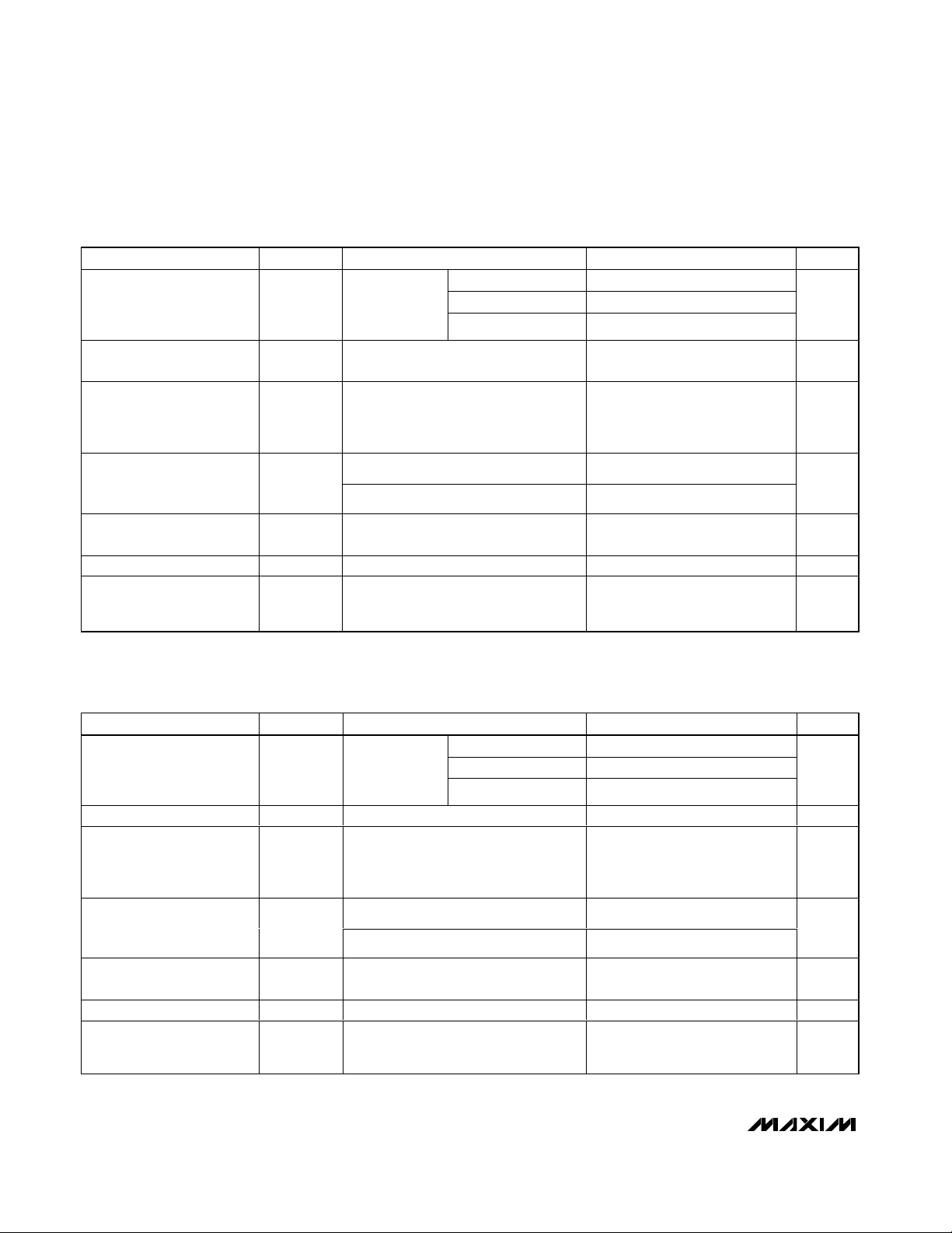
ELECTRICAL CHARACTERISTICS—MAX6138_30 (3.0V)
(IR= 100µA, TA= -40°C to +85°C, unless otherwise noted. Typical values are at TA= +25°C.) (Note 1)
ELECTRICAL CHARACTERISTICS—MAX6138_33 (3.3V)
(IR= 100µA, TA= -40°C to +85°C, unless otherwise noted. Typical values are at TA= +25°C.) (Note 1)
PARAMETER SYMBOL CONDITIONS MIN TYP MAX UNITS
MAX6138A (0.1%) 2.9970 3.0000 3.0030
Reverse Breakdown
Voltage (Note 2)
Minimum Operating
Current
Reverse Voltage
Temperature Coefficient
(Notes 2, 3)
V
R
I
RMIN
TC 4 25 ppm/°C
TA = +25°C
MAX6138B (0.2%) 2.9940 3.0000 3.0060
MAX6138C (0.5%) 2.9850 3.0000 3.0150
45 65 µA
V
Reverse Breakdown
Voltage Change with
Operating Current Change
Reverse Dynamic
Impedance (Note 3)
Wideband Noise e
Reverse Breakdown
Voltage Long-Term
Stability
∆V
∆V
/∆I
R
Z
R
N
R
I
≤ IR ≤ 1mA 0.3 1.0
RMIN
R
1mA ≤ IR ≤ 15mA 2.5 8.0
IR = 1mA, f =120Hz, IAC = 0.1I
10Hz ≤ f ≤ 10kHz 45 µV
t = 1000h 120 ppm
R
0.3 0.8 Ω
PARAMETER SYMBOL CONDITIONS MIN TYP MAX UNITS
MAX6138A (0.1%) 3.2967 3.3000 3.3033
Reverse Breakdown
Voltage (Note 2)
M i ni m um Op er ati ng C ur r ent I
Reverse Voltage
Temperature Coefficient
(Notes 2, 3)
Reverse Breakdown
Voltage Change with
Operating Current Change
Reverse Dynamic
Impedance (Note 3)
Wideband Noise e
Reverse Breakdown
Voltage Long-Term
Stability
∆V
V
R
RMIN
TC 4 25 ppm/°C
/∆I
R
Z
R
N
∆V
R
TA = +25°C
I
≤ IR ≤ 1mA 0.3 1.0
RMIN
R
1mA ≤ IR ≤ 15mA 8.0
IR = 1mA, f =120Hz, IAC = 0.1I
10Hz ≤ f ≤ 10kHz 50 µV
t = 1000h 120 ppm
MAX6138B (0.2%) 3.2934 3.3000 3.3066
MAX6138C (0.5%) 3.2835 3.3000 3.3165
45 67 µA
R
0.3 0.8 Ω
mV
RMS
V
mV
RMS
Page 5

MAX6138
0.1%, 25ppm, SC70 Shunt Voltage Reference
with Multiple Reverse Breakdown Voltages
_______________________________________________________________________________________ 5
ELECTRICAL CHARACTERISTICS—MAX6138_41 (4.096V)
(IR= 100µA, TA= -40°C to +85°C, unless otherwise noted. Typical values are at TA= +25°C.) (Note 1)
ELECTRICAL CHARACTERISTICS—MAX6138_50 (5.0V)
(IR= 100µA, TA= -40°C to +85°C, unless otherwise noted. Typical values are at TA= +25°C.) (Note 1)
Note 1: All devices are 100% production tested at +25°C and are guaranteed by correlation for T
A
= T
MAX
to T
MIN
, as specified.
Note 2: TC is measured by the “box” method, i.e. (V
MAX
- V
MIN
) / (T
MAX
- T
MIN
)
Note 3: Guaranteed by design.
PARAMETER SYMBOL CONDITIONS MIN TYP MAX UNITS
Reverse Breakdown
Voltage (Note 2)
Minimum Operating
Current
Reverse Voltage
Temperature Coefficient
(Notes 2, 3)
Reverse Breakdown
Voltage Change with
Operating Current Change
Reverse Dynamic
Impedance (Note 3)
Wideband Noise e
Reverse Breakdown
Voltage Long-Term
Stability
I
RMIN
∆VR/∆I
V
R
TC 4 25 ppm/°C
R
Z
R
N
∆V
R
= +25°C
T
A
I
≤ IR ≤ 1mA 0.5 1.2
RMIN
1mA ≤ I
I
R
10Hz ≤ f ≤ 10kHz 64 µV
t = 1000h 120 ppm
≤ 15mA 3.0 10.0
R
= 1mA, f = 120Hz, IAC = 0.1I
MAX6138A (0.1%) 4.0919 4.0960 4.1001
MAX6138B (0.2%) 4.0878 4.0960 4.1042
MAX6138C (0.5%) 4.0755 4.0960 4.1165
50 73 µA
R
0.5 1.0 Ω
V
mV
RMS
PARAMETER SYMBOL CONDITIONS MIN TYP MAX UNITS
Reverse Breakdown
Voltage (Note 2)
M i ni m um Op er ati ng C ur r ent I
Reverse Voltage
Temperature Coefficient
(Notes 2, 3)
Reverse Breakdown
Voltage Change with
Operating Current Change
Reverse Dynamic
Impedance (Note 3)
Wideband Noise e
Rever se Br eakd ow n
V ol tag e Long - Ter m S tab i l i ty
V
R
RMIN
TC 4 25 ppm/°C
∆V
/∆I
R
Z
R
N
∆V
R
TA = +25°C
I
≤ IR ≤ 1mA 0.5 1.4
RMIN
R
1mA ≤ IR ≤ 15mA 3.5 12.0
IR = 1mA, f = 120Hz, IAC = 0.1I
10Hz ≤ f ≤ 10kHz 80 µV
t = 1000h 120 ppm
MAX6138A (0.1%) 4.9950 5.0000 5.0050
MAX6138B (0.2%) 4.9900 5.0000 5.0100
MAX6138C (0.5%) 4.9750 5.0000 5.0250
54 80 µA
0.5 1.1 Ω
R
V
mV
RMS
Page 6

4.996
4.998
4.997
5.000
4.999
5.002
5.001
5.003
-40 0 20-20 40 60 80
MAX6138_50
TEMPERATURE DRIFT
MAX6138 toc04
TEMPERATURE (°C)
REVERSE VOLTAGE (V)
3 TYPICAL PARTS
0
1.5
1.0
0.5
2.0
2.5
3.0
3.5
4.0
4.5
5.0
0510 2015
MAX6138_12
REVERSE VOLTAGE vs. I
SHUNT
MAX61438 toc05
I
SHUNT
(mA)
REVERSE VOLTAGE CHANGE (mV)
TA = +85°C
TA = +25°C
TA = -40°C
MAX6138
0.1%, 25ppm, SC70 Shunt Voltage Reference
with Multiple Reverse Breakdown Voltages
6 _______________________________________________________________________________________
Typical Operating Characteristics
(IR= 100µA, TA= +25°C, unless otherwise noted.)
0
2
1
4
3
5
6
04020 60 80 100
REVERSE CHARACTERISTICS AND
MINIMUM OPERATING CURRENT
MAX6138 toc01
REVERSE CURRENT (µA)
REVERSE VOLTAGE (V)
MAX6138_50
MAX6138_41
MAX6138_30
MAX6138_25
MAX6138_12
MAX6138_20
1.2215
1.2210
1.2205
1.2200
1.2195
-40 20-20 0 40 60 80
MAX6138_12
TEMPERATURE DRIFT
MAX6138 toc02
TEMPERATURE (°C)
REVERSE VOLTAGE (V)
3 TYPICAL PARTS
2.4890
2.4990
2.4895
2.5000
2.4995
2.5010
2.5005
2.5015
-40 0 20-20 40 60 80
MAX6138_25
TEMPERATURE DRIFT
MAX6138 toc03
TEMPERATURE (°C)
REVERSE VOLTAGE (V)
3 TYPICAL PARTS
Page 7

MAX6138
0.1%, 25ppm, SC70 Shunt Voltage Reference
with Multiple Reverse Breakdown Voltages
_______________________________________________________________________________________ 7
Typical Operating Characteristics (continued)
(IR= 100µA, TA= +25°C, unless otherwise noted.)
Figure 1. Load-Transient Circuit
MAX6138_25
REVERSE VOLTAGE vs. I
5.0
4.5
TA = +25°C
I
SHUNT
TA = +85°C
4.0
3.5
3.0
2.5
2.0
1.5
1.0
REVERSE VOLTAGE CHANGE (mV)
0.5
0
0 5 10 2015
SHUNT
TA = -40°C
(mA)
MAX6138_12
LOAD-TRANSIENT RESPONSE
MAX6138 toc08
MAX6138_50
MAX61438 toc06
+25µA
-25µA
REVERSE VOLTAGE vs. I
5.0
4.5
4.0
3.5
3.0
2.5
2.0
1.5
1.0
REVERSE VOLTAGE CHANGE (mV)
0.5
0
0 5 10 2015
TA = +25°C
I
TA = +85°C
SHUNT
MAX6138_25
LOAD-TRANSIENT RESPONSE
SHUNT
MAX61438 toc07
TA = -40°C
(mA)
MAX6138 toc09
+25µA
-25µA
V
AC-COUPLED
R
10mV/div
I
= 100µA ±25µA
SHUNT
= 48k
R
L
V
AC-COUPLED
R
10mV/div
4µs/div
Ω
I
SHUNT
+
V
B
-
V
1kΩ
R
R
I
= 100µA
SHUNT
= 100k
R
L
+ I
LOAD
L
V
GEN
10µs/div
Ω
Page 8

MAX6138
0.1%, 25ppm, SC70 Shunt Voltage Reference
with Multiple Reverse Breakdown Voltages
8 _______________________________________________________________________________________
Typical Operating Characteristics (continued)
(IR= 100µA, TA= +25°C, unless otherwise noted.)
Figure 2. Startup Characteristics Test Circuit
MAX6138_50
LOAD-TRANSIENT RESPONSE
MAX6138 toc10
+25µA
MAX6138_12
LOAD-TRANSIENT RESPONSE
MAX6138 toc11
+250µA
I
= 100µA
SHUNT
= 100k
R
L
I
SHUNT
= 10k
R
L
40µs/div
Ω
MAX6138_25
LOAD-TRANSIENT RESPONSE
10µs/div
= 1mA
Ω
MAX6138 toc12
-25µA
V
AC-COUPLED
R
20mV/div
+250µA
-250µA
V
AC-COUPLED
R
10mV/div
10µs/div
I
= 1mA
SHUNT
= 10k
R
Ω
L
MAX6138_50
LOAD-TRANSIENT RESPONSE
I
SHUNT
= 10k
R
L
= 1mA
40µs/div
Ω
MAX6138 toc13
-250µA
V
AC-COUPLED
R
2.0mV/div
+250µA
-250µA
V
AC-COUPLED
R
2mV/div
R
S
V
1Hz RATE
50%
DUTY CYCLE
IN
V
R
Page 9

MAX6138
0.1%, 25ppm, SC70 Shunt Voltage Reference
with Multiple Reverse Breakdown Voltages
_______________________________________________________________________________________ 9
Typical Operating Characteristics (continued)
(IR= 100µA, TA= +25°C, unless otherwise noted.)
I
SHUNT
= 1k
R
L
MAX6138_12
LOAD-TRANSIENT RESPONSE
10µs/div
= 10mA
Ω
MAX6138 toc14
MAX6138_50
LOAD-TRANSIENT RESPONSE
MAX6138 toc16
MAX6138_25
+2.5mA
-2.5mA
V
AC-COUPLED
R
100mV/div
+2.5mA
-2.5mA
LOAD-TRANSIENT RESPONSE
10µs/div
I
= 10mA
SHUNT
= 1k
R
Ω
L
MAX6138_12
STARTUP CHARACTERISTICS
V
IN
MAX6138 toc15
MAX6138 toc17
+2.5mA
-2.5mA
V
AC-COUPLED
R
5mV/div
5V
0
1.2V
V
AC-COUPLED
R
100mV/div
V
OUT
40µs/div
I
= 10mA
SHUNT
= 1k
R
Ω
L
MAX6138_25
STARTUP CHARACTERISTICS
V
IN
V
OUT
2µs/div
I
= 100µA
SHUNT
= 30kΩ
R
S
MAX6138 toc18
5V
V
IN
0
2V
0
V
OUT
I
SHUNT
= 16kΩ
R
S
MAX6138_50
STARTUP CHARACTERISTICS
100µs/div
= 100µA
I
SHUNT
R
S
= 100µA
= 30k
MAX6138 toc19
200ns/div
Ω
1000
5V
100
0
5V
0
10
IMPEDANCE (Ω)
1
0.1
100 10k1k 100k 1M
0
MAX6138_12
OUTPUT IMPEDANCE
vs. FREQUENCY
150µA
IR =
IR = 1mA
FREQUENCY (Hz)
CL = 0
MAX6138 toc20
CL = 1µF
Page 10

MAX6138
0.1%, 25ppm, SC70 Shunt Voltage Reference
with Multiple Reverse Breakdown Voltages
10 ______________________________________________________________________________________
Typical Operating Characteristics (continued)
(IR= 100µA, TA= +25°C, unless otherwise noted.)
0.1 101 100 1000
MAX6138_25
OUTPUT IMPEDANCE vs. FREQUENCY
MAX61438 toc21
FREQUENCY (Hz)
IMPEDANCE (Ω)
1000
0.1
1
10
100
IR = 150µA
IR = 1mA
CL = 1µF
CL = 0
0.1 101 100 1000
MAX6138_50
OUTPUT IMPEDANCE vs. FREQUENCY
MAX6138 toc22
FREQUENCY (Hz)
IMPEDANCE (Ω)
100
0.1
1
10
IR = 150µA
IR = 1mA
CL = 0
CL = 1µF
1 100 10k
MAX6138_12
NOISE vs. FREQUENCY
MAX6138 toc23
FREQUENCY (Hz)
NOISE (nV√Hz)
10,000
100
1000
10 1k
110010 1k 10k
MAX6138_25
NOISE vs. FREQUENCY
MAX6138 toc24
FREQUENCY (Hz)
10,000
100
1000
NOISE (nV/√Hz)
1 10010 1k 10k
MAX6138_50
NOISE vs. FREQUENCY
MAX6138 toc25
FREQUENCY (Hz)
10,000
100
1000
NOISE (nV/√Hz)
Page 11

MAX6138
0.1%, 25ppm, SC70 Shunt Voltage Reference
with Multiple Reverse Breakdown Voltages
______________________________________________________________________________________ 11
Detailed Description
The MAX6138 shunt reference uses the bandgap principle to produce a stable, accurate voltage. The device
behaves similarly to an ideal zener diode; a fixed voltage is maintained across its output terminals when
biased with 60µA to 15mA of reverse current. The
MAX6138 behaves similarly to a silicon diode when
biased with forward currents up to 10mA.
Figure 3 shows a typical operating circuit. The
MAX6138 is ideal for providing a stable reference from
a high-voltage power supply.
Applications Information
The MAX6138’s internal pass transistor is used to maintain a constant output voltage (V
SHUNT
) by sinking the
necessary amount of current across a source resistor.
The source resistance (RS) is determined from the load
current (I
LOAD
) range, supply voltage (VS) variations,
V
SHUNT
, and desired quiescent current.
Choose the value of R
S
when VSis at a minimum and
I
LOAD
is at a maximum. Maintain a minimum I
SHUNT
of
60µA at all times. The RSvalue should be large enough
to keep I
SHUNT
less than 15mA for proper regulation
when V
S
is maximum and I
LOAD
is at a minimum. To
prevent damage to the device, I
SHUNT
should never
exceed 20mA.
Therefore, the value of RSis bounded by the following
equation:
[V
S(MIN)
- VR] / [60µA + I
LOAD(MAX)
] > RS>
[V
S(MAX
) - VR] / [20mA + I
LOAD(MIN)
]
Choosing a larger resistance minimizes the total power
dissipation in the circuit by reducing the shunt current
(P
D(TOTAL)
= VSX I
SHUNT
). Provide a safety margin to
incorporate the worst-case tolerance of the resistor
used. Ensure that the resistor’s power rating is adequate, using the following general power equation:
PDR= I
SHUNT
✕
(V
S(MAX)
- V
SHUNT
)
Output Capacitance
The MAX6138 does not require an external capacitor
for operational stability and is stable for any output
capacitance.
Temperature Performance
The MAX6138 typically exhibits an output voltage temperature coefficient within ±4ppm/°C. The polarity of
the temperature coefficient may be different from one
device to another; some may have positive coefficients,
and others may have negative coefficients.
Chip Information
TRANSISTOR COUNT: 70
PROCESS: BiCMOS
Pin Description
Figure 3. Typical Operating Circuit
PIN NAME FUNCTION
1 + Positive Terminal of the Shunt Reference
2 - Negative Terminal of the Shunt Reference
3 N.C. No Connection. Leave this pin unconnected or connect to Pin 2.
V
S
I
+ I
SHUNT
R
S
I
SHUNT
LOAD
I
LOAD
MAX6138
V
R
Page 12

MAX6138
0.1%, 25ppm, SC70 Shunt Voltage Reference
with Multiple Reverse Breakdown Voltages
12 ______________________________________________________________________________________
Ordering Information
OUTPUT
PART
MAX6138AEXR12-T 1.2205 0.1 -40°C to +85°C 3 SC70-3 AEW
MAX6138BEXR12-T 1.2205 0.2 -40°C to +85°C 3 SC70-3 AEX
MAX6138CEXR12-T 1.2205 0.5 -40°C to +85°C 3 SC70-3 AEY
MAX6138AEXR21-T 2.0480 0.1 -40°C to +85°C 3 SC70-3 AFA
MAX6138BEXR21-T 2.0480 0.2 -40°C to +85°C 3 SC70-3 AFB
MAX6138CEXR21-T 2.0480 0.5 -40°C to +85°C 3 SC70-3 AFC
MAX6138AEXR25-T 2.5000 0.1 -40°C to +85°C 3 SC70-3 AFE
MAX6138BEXR25-T 2.5000 0.2 -40°C to +85°C 3 SC70-3 AFF
MAX6138CEXR25-T 2.5000 0.5 -40°C to +85°C 3 SC70-3 AFG
MAX6138AEXR30-T 3.0000 0.1 -40°C to +85°C 3 SC70-3 AFI
MAX6138BEXR30-T 3.0000 0.2 -40°C to +85°C 3 SC70-3 AFJ
MAX6138CEXR30-T 3.0000 0.5 -40°C to +85°C 3 SC70-3 AFK
MAX6138AEXR33-T 3.3000 0.1 -40°C to +85°C 3 SC70-3 ANG
MAX6138BEXR33-T 3.3000 0.2 -40°C to +85°C 3 SC70-3 ANH
MAX6138CEXR33-T 3.3000 0.5 -40°C to +85°C 3 SC70-3 ANI
MAX6138AEXR41-T 4.0960 0.1 -40°C to +85°C 3 SC70-3 AFM
MAX6138BEXR41-T 4.0960 0.2 -40°C to +85°C 3 SC70-3 AFN
MAX6138CEXR41-T 4.0960 0.5 -40°C to +85°C 3 SC70-3 AFO
MAX6138AEXR50-T 5.0000 0.1 -40°C to +85°C 3 SC70-3 AFQ
MAX6138BEXR50-T 5.0000 0.2 -40°C to +85°C 3 SC70-3 AFR
MAX6138CEXR50-T 5.0000 0.5 -40°C to +85°C 3 SC70-3 AFS
VOLTAGE
(V)
INITIAL
ACCURACY
(%)
TEMP RANGE PIN-PACKAGE TOP MARK
Page 13

MAX6138
0.1%, 25ppm, SC70 Shunt Voltage Reference
with Multiple Reverse Breakdown Voltages
Maxim cannot assume responsibility for use of any circuitry other than circuitry entirely embodied in a Maxim product. No circuit patent licenses are
implied. Maxim reserves the right to change the circuitry and specifications without notice at any time.
Maxim Integrated Products, 120 San Gabriel Drive, Sunnyvale, CA 94086 408-737-7600 ____________________ 13
© 2004 Maxim Integrated Products Printed USA is a registered trademark of Maxim Integrated Products.
Package Information
SC70, 3L.EPS
 Loading...