

Page 1
General Description
The MAX6133 high-precision, low-power, low-dropout
voltage reference features a low 3ppm/°C (max) temperature coefficient and a low dropout voltage (200mV,
max). This series-mode device features bandgap technology for low-noise performance and excellent accuracy. Load regulation specifications are guaranteed for
source currents up to 15mA. The laser-trimmed, highstability thin-film resistors, together with post-package
trimming, guarantee an excellent initial accuracy specification (0.04%, max). The MAX6133 is a series voltage
reference and consumes only 40µA of supply current
(virtually independent of supply voltage). Series-mode
references save system power and use minimal external
components compared to 2-terminal shunt references.
The MAX6133 is available in 8-pin µMAX and SO packages. The unique blend of tiny packaging and excellent
precision performance make these parts ideally suited
for portable and communication applications.
Applications
Precision Regulators
A/D and D/A Converters
Power Supplies
High-Accuracy Industrial and Process Control
Hand-Held Instruments
Features
♦ Low Temperature Coefficient
3ppm/°C (max), SO
5ppm/°C (max), µMAX
♦ Tiny 5mm
✕ 3mm µMAX Package
♦ Low 200mV (max) Dropout Voltage
♦ Low 40µA Quiescent Current
♦ ±0.04% (max) Initial Accuracy
♦ Low 16µV
P-P
Noise (0.1Hz to 10Hz) (2.5V Output)
♦ 15mA Output Source-Current Capability
♦ Wide 2.7V to 12.6V Supply Voltage
♦ Excellent Line (30µV/V, max) and
Load (0.05mV/mA, max) Regulation
MAX6133
3ppm/°C, Low-Power, Low-Dropout
Voltage Reference
________________________________________________________________ Maxim Integrated Products 1
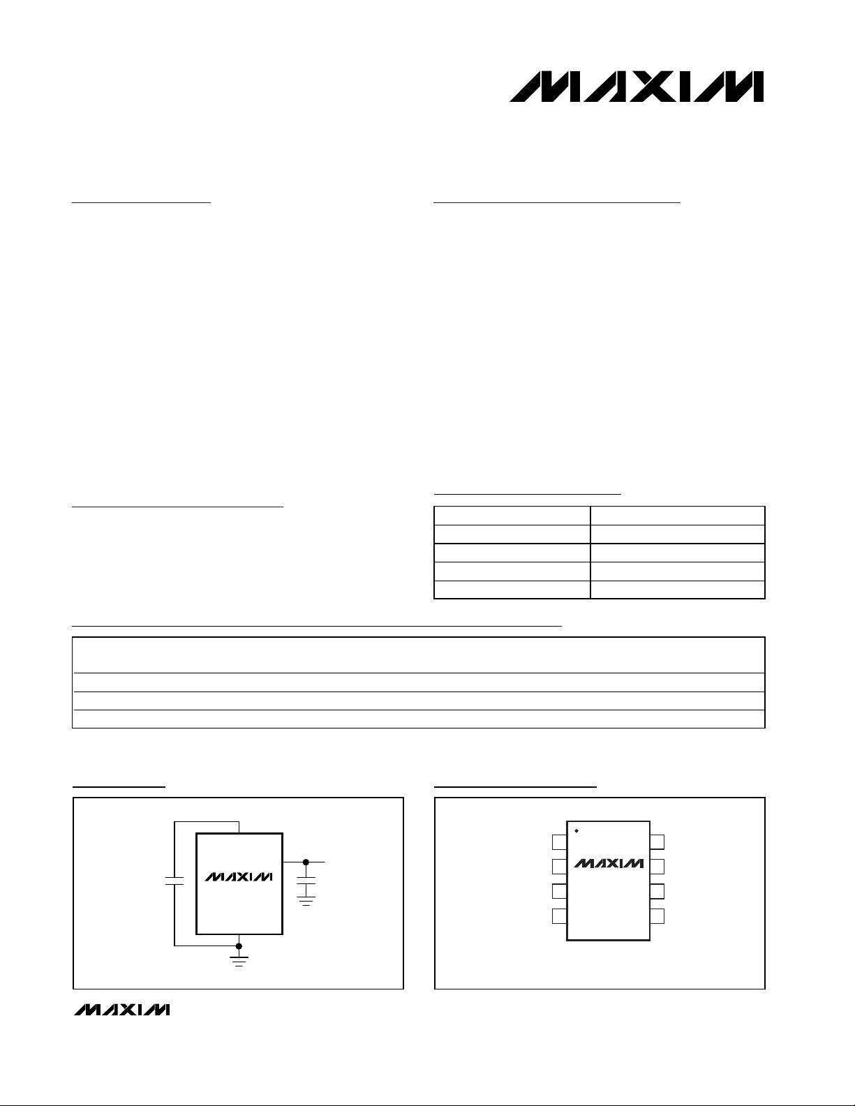
Pin Configuration
Ordering Information
MAX6133
OUT
SUPPLY INPUT
GND
*INPUT CAPACITORS ARE OPTIONAL.
IN
0.1µF*
REFERENCE
OUTPUT
0.1µF
Typical Operating Circuit
19-2266; Rev 2; 6/03
For pricing, delivery, and ordering information, please contact Maxim/Dallas Direct! at
1-888-629-4642, or visit Maxim’s website at www.maxim-ic.com.
Note: Two-number part suffix indicates output voltage option.
Selector Guide
SUFFIX VOLTAGE OUTPUT
25 2.500V
30 3.000V
41 4.096V
50 5.000V
PART TEMP RANGE PIN-PACKAGE
MAX6133A_ _ -40°C to +125°C 8 µMAX 0.06 5
MAX6133AASA_ _ -40°C to +125°C 8 SO 0.04 3
MAX6133BASA_ _ -40°C to +125°C 8 SO 0.08 5
MAXIMUM INITIAL
ACCURACY (%)
TOP VIEW
*INTERNALLY CONNECTED, DO NOT CONNECT.
MAXIMUM TEMPCO
(ppm/°C, -40°C to +85°C)
N.C.
N.C.
1
2
MAX6133
3
4
SO/µMAX
87I.C.*
N.C.IN
OUT
6
I.C.*GND
5
Page 2
MAX6133
3ppm/°C, Low-Power, Low-Dropout
Voltage Reference
2 _______________________________________________________________________________________
ABSOLUTE MAXIMUM RATINGS
ELECTRICAL CHARACTERISTICS—MAX6133_25 (V
OUT
= 2.500V)
(VIN= 5V, C
LOAD
= 0.1µF, I
OUT
= 0, TA= T
MIN
to T
MAX
. Typical values are at TA = +25°C, unless otherwise noted.)
Stresses beyond those listed under “Absolute Maximum Ratings” may cause permanent damage to the device. These are stress ratings only, and functional
operation of the device at these or any other conditions beyond those indicated in the operational sections of the specifications is not implied. Exposure to
absolute maximum rating conditions for extended periods may affect device reliability.
Voltage (with Respect to GND)
IN ........................................................................-0.3V to +13V
OUT..............................................-0.3V to +6V or (V
IN
+ 0.3V)
OUT Short Circuit to IN or GND Duration ...............................60s
Continuous Power Dissipation (T
A
= +70°C)
8-Pin µMAX (derate 5.5mW/°C above +70°C) .............362mW
8-Pin SO (derate 5.88mW/°C above +70°C)................471mW
Operating Temperature Range .........................-40°C to +125°C
Storage Temperature Range .............................-65°C to +150°C
Junction Temperature......................................................+150°C
Lead Temperature (soldering, 10s) .................................+300°C
PARAMETER SYMBOL CONDITIONS MIN TYP MAX UNITS
Output Voltage V
Output Voltage
Accuracy
Output Voltage
Temperature
Coefficient (Note 1)
Input Voltage Range V
Line Regulation ∆V
Load Regulation ∆V
Dropout Voltage
(Note 2)
Quiescent Supply
Current
Output Short-Circuit
Current
Output Voltage Noise e
Turn-On Settling Time t
Thermal Hysteresis
(Note 3)
Long-Term Stability ∆t = 1000 hours
OUT
TCV
OUT
IN
/∆VIN2.7V ≤ VIN ≤ 12.6V 2 30 µV/V
OUT
/∆I
OUT
OUT
V
DO
I
IN
I
SC
n
ON
TA = +25°C
T
= +25°C
A
A grade SO
B grade SO
µMAX
Inferred from line regulation 2.7 12.6 V
-100µA ≤ I
∆V
OUT
∆V
OUT
TA = +25°C4060
TA = -40°C to +125°C85
Short to GND: V
Short to VIN: V
0.1Hz ≤ f ≤ 10Hz 16 µV
10Hz ≤ f ≤ 1kHz 12 µV
V
settles to ±0.01% of final value 500 µs
OUT
A grade SO 2.4990 2.5000 2.5010
B grade SO 2.4980 2.5000 2.5020
µMAX 2.4985 2.5000 2.5015
A grade SO -0.04 +0.04
B grade SO -0.08 +0.08
µMAX -0.06 +0.06
TA = -40°C to +85°C13
T
= -40°C to +125°C47
A
TA = -40°C to +85°C35
T
= -40°C to +125°C510
A
TA = -40°C to +85°C15
T
= -40°C to +125°C27
A
≤ 15mA 0.003 0.05 mV/mA
OUT
= 0.1%, I
= 0.1%, I
= 1mA 0.02 0.2
OUT
= 10mA 0.2 0.4
OUT
= 0V 90
OUT
= V
OUT
IN
SO 40
µMAX 145
-2
120 ppm
V
%
ppm/°C
V
µA
mA
P-P
RMS
ppm
Page 3
MAX6133
3ppm/°C, Low-Power, Low-Dropout
Voltage Reference
_______________________________________________________________________________________ 3
ELECTRICAL CHARACTERISTICS—MAX6133_30 (V
OUT
= 3.0000V)
(VIN= 5V, C
LOAD
= 0.1µF, I
OUT
= 0, TA= T
MIN
to T
MAX
. Typical values are at TA = +25°C, unless otherwise noted.)
PARAMETER SYMBOL CONDITIONS MIN TYP MAX UNITS
Output Voltage V
Output Voltage
Accuracy
Output Voltage
Temperature
Coefficient (Note 1)
Input Voltage Range V
Line Regulation ∆V
Load Regulation ∆V
Dropout Voltage
(Note 2)
Quiescent Supply
Current
Output Short-Circuit
Current
Output Voltage Noise e
Turn-On Settling Time t
Thermal Hysteresis
(Note 3)
Long-Term Stability ∆t = 1000 hours
OUT
TCV
OUT
IN
/∆VIN3.2V ≤ VIN ≤ 12.6V 2 30 µV/V
OUT
/∆I
OUT
OUT
V
DO
I
IN
I
SC
n
ON
TA = +25°C
= +25°C
T
A
A grade SO
B grade SO
µMAX
Inferred from line regulation 3.2 12.6 V
-100µA ≤ I
∆V
OUT
∆V
OUT
TA = +25°C4060
TA = -40°C to +125°C85
Short to GND: V
Short to VIN: V
0.1Hz ≤ f ≤ 10Hz 24 µV
10Hz ≤ f ≤ 1kHz 15 µV
V
settles to ±0.01% of final value 600 µs
OUT
A grade SO 2.9988 3.0000 3.0012
B grade SO 2.9976 3.0000 3.0024
µMAX 2.9982 3.0000 3.0018
A grade SO -0.04 +0.04
B grade SO -0.08 +0.08
µMAX -0.06 +0.06
TA = -40°C to +85°C13
= -40°C to +125°C47
T
A
TA = -40°C to +85°C35
= -40°C to +125°C510
T
A
TA = -40°C to +85°C15
T
= -40°C to +125°C27
A
≤ 15mA 0.003 0.06 mV/mA
OUT
= 0.1%, I
= 0.1%, I
= 1mA 0.01 0.2
OUT
= 10mA 0.2 0.4
OUT
= 0V 90
OUT
= V
OUT
IN
SO 40
µMAX 145
-2
120 ppm
V
%
ppm/°C
V
µA
mA
P-P
RMS
ppm
Page 4
MAX6133
3ppm/°C, Low-Power, Low-Dropout
Voltage Reference
4 _______________________________________________________________________________________
ELECTRICAL CHARACTERISTICS—MAX6133_41 (V
OUT
= 4.096V)
(VIN= 5V, C
LOAD
= 0.1µF, I
OUT
= 0, TA= T
MIN
to T
MAX
. Typical values are at TA = +25°C, unless otherwise noted.)
PARAMETER SYMBOL CONDITIONS MIN TYP MAX UNITS
Output Voltage V
Output Voltage
Accuracy
Output Voltage
Temperature
Coefficient (Note 1)
Input Voltage Range V
Line Regulation ∆V
Load Regulation ∆V
Dropout Voltage
(Note 2)
Quiescent Supply
Current
Output Short-Circuit
Current
Output Voltage Noise e
Turn-On Settling Time t
Thermal Hysteresis
(Note 3)
Long-Term Stability ∆t = 1000 hours
OUT
TCV
OUT
IN
/∆VIN4.2V ≤ VIN ≤ 12.6V 2 40 µV/V
OUT
/∆I
OUT
OUT
V
DO
I
IN
I
SC
n
ON
TA = +25°C
= +25°C
T
A
A grade SO
B grade SO
µMAX
Inferred from line regulation 4.2 12.6 V
-100µA ≤ I
∆V
OUT
∆V
OUT
TA = +25°C4565
TA = -40°C to +125°C85
Short to GND: V
Short to VIN: V
0.1Hz ≤ f ≤ 10Hz 32 µV
10Hz ≤ f ≤ 1kHz 22 µV
V
settles to ±0.01% of final value 800 µs
OUT
A grade SO 4.0943 4.0960 4.0977
B grade SO 4.0927 4.0960 4.0993
µMAX 4.0935 4.0960 4.0985
A grade SO -0.04 +0.04
B grade SO -0.08 +0.08
µMAX -0.06 +0.06
TA = -40°C to +85°C13
T
A
TA = -40°C to +85°C35
T
A
TA = -40°C to +85°C15
T
A
≤ 15mA 0.003 0.08 mV/mA
OUT
= 0.1%, I
= 0.1%, I
= 1mA 0.01 0.2
OUT
= 10mA 0.2 0.4
OUT
= 0V 90
OUT
= V
OUT
IN
SO 40
µMAX 145
V
%
= -40°C to +125°C47
= -40°C to +125°C510
= -40°C to +125°C27
-2
120 ppm
ppm/°C
V
µA
mA
P-P
RMS
ppm
Page 5

MAX6133
3ppm/°C, Low-Power, Low-Dropout
Voltage Reference
_______________________________________________________________________________________ 5
ELECTRICAL CHARACTERISTICS—MAX6133_50 (V
OUT
= 5.000V)
(VIN= 5.5V, C
LOAD
= 0.1µF, I
OUT
= 0, TA= T
MIN
to T
MAX
. Typical values are at TA = +25°C, unless otherwise noted.)
Note 1: The MAX6133 is 100% drift-tested for TA= T
MIN
to T
MAX
, as specified.
Note 2: Dropout Voltage is the minimum voltage at which V
OUT
changes ≤ 0.1% from V
OUT
at VIN= 5V (VIN= 5.5V for V
OUT
= 5V).
Note 3: Thermal Hysteresis is defined as the change in the initial +25°C output voltage after cycling the device from T
MAX
to T
MIN
.
PARAMETER SYMBOL CONDITIONS MIN TYP MAX UNITS
Output Voltage V
Output Voltage
Accuracy
Output Voltage
Temperature
Coefficient (Note 1)
Input Voltage Range V
Line Regulation ∆V
Load Regulation ∆V
Dropout Voltage
(Note 2)
Quiescent Supply
Current
Output Short-Circuit
Current
Output Voltage Noise e
Turn-On Settling Time t
Thermal Hysteresis
(Note 3)
Long-Term Stability ∆t = 1000 hours
TA = +25°C
T
A grade SO
B grade SO
µMAX
Inferred from line regulation 5.2 12.6 V
/∆VIN5.2V ≤ VIN ≤ 12.6V 2 50 µV/V
-100µA ≤ I
OUT
∆V
∆V
TA = +25°C4060
TA = -40°C to +125°C85
Short to GND: V
Short to VIN: V
0.1Hz ≤ f ≤ 10Hz 40 µV
10Hz ≤ f ≤ 1kHz 26 µV
V
TCV
OUT
OUT
V
OUT
IN
DO
I
IN
I
SC
ON
OUT
/∆I
n
= +25°C
A
= 0.1%, I
OUT
= 0.1%, I
OUT
settles to ±0.01% of final value 1000 µs
OUT
A grade SO 4.9980 5.0000 5.0020
B grade SO 4.9960 5.0000 5.0040
µMAX 4.9970 5.0000 5.0030
A grade SO -0.04 +0.04
B grade SO -0.08 +0.08
µMAX -0.06 +0.06
TA = -40°C to +85°C13
= -40°C to +125°C47
T
A
TA = -40°C to +85°C35
= -40°C to +125°C510
T
A
TA = -40°C to +85°C15
T
= -40°C to +125°C27
A
≤ 15mA 0.01 0.10 mV/mA
OUT
= 1mA 0.02 0.2
OUT
= 10mA 0.2 0.4
OUT
= 0V 90
OUT
= V
OUT
IN
SO 40
µMAX 145
-2
120 ppm
V
%
ppm/°C
V
µA
mA
P-P
RMS
ppm
Page 6

MAX6133
3ppm/°C, Low-Power, Low-Dropout
Voltage Reference
6 _______________________________________________________________________________________
Typical Operating Characteristics
(VIN= 5V, I
OUT
= 0, TA = +25°C, unless otherwise noted.) (Note 4)
SUPPLY CURRENT vs. INPUT VOLTAGE
(V
OUT
= 2.5V)
MAX6133 toc09
INPUT VOLTAGE (V)
SUPPLY CURRENT (µA)
12119 103 4 5 6 7 81 2
15
30
45
60
75
90
105
120
135
150
0
013
TA = +85°C
TA = +125°C
TA = +25°C
TA = -40°C
-120
-80
-100
-60
-40
-20
0
0.0001 0.010.001 0.1 10 100 1000
POWER-SUPPLY REJECTION RATIO
vs. FREQUENCY (V
OUT
= 5V)
MAX6133 toc08
FREQUENCY (kHz)
PSRR (dB)
1
VIN = 5.5V
POWER-SUPPLY REJECTION RATIO
vs. FREQUENCY (V
OUT
= 2.5V)
FREQUENCY (kHz)
0.0001 0.1 10 1000.001 0.01 1000
PSRR (dB)
0
-120
-100
-80
-60
-40
-20
MAX6133 toc07
1
DROPOUT VOLTAGE vs. OUTPUT CURRENT
(V
OUT
= 5V)
MAX6133 toc06
OUTPUT CURRENT (mA)
DROPOUT VOLTAGE (mV)
181612 144 6 8 102
50
100
150
200
250
300
350
400
450
500
550
600
0
020
TA = +85°C
TA = +125°C
TA = +25°C
TA = -40°C
VIN = 5.5V
DROPOUT VOLTAGE vs. OUTPUT CURRENT
(V
OUT
= 2.5V)
MAX6133 toc05
OUTPUT CURRENT (mA)
DROPOUT VOLTAGE (mV)
18161412108642
100
200
300
400
500
600
700
0
020
TA = +85°C
TA = +125°C
TA = +25°C
TA = -40°C
LOAD REGULATION
(V
OUT
= 5V)
MAX6133 toc04
OUTPUT CURRENT (mA)
OUTPUT VOLTAGE (V)
18
2
46 10
12 14816
4.9985
4.9990
4.9995
5.0000
5.0005
5.0010
5.0015
5.0020
4.9980
020
TA = +25°C
VIN = 5.5V
TA = +125°C
TA = +85°C
TA = -40°C
LOAD REGULATION
(V
OUT
= 2.5V)
MAX6133 toc03
OUTPUT CURRENT (mA)
OUTPUT VOLTAGE (V)
201814 1646810122
2.5005
2.5010
2.4990
2.4995
2.5000
2.5015
2.5020
2.5025
2.5030
2.5035
2.5040
0
TA = +25°C
TA = +125°C
TA = +85°C
TA = -40°C
OUTPUT VOLTAGE vs. TEMPERATURE
(V
OUT
= 5V)
MAX6133 toc02
TEMPERATURE (°C)
OUTPUT VOLTAGE (V)
1109565 80-10 5 20 35 50-25
4.9985
4.9990
4.9995
5.0000
5.0005
5.0010
4.9980
-40 125
3 TYPICAL UNITS
V
IN
= 5.5V
OUTPUT VOLTAGE vs. TEMPERATURE
(V
OUT
= 2.5V)
MAX6133 toc01
TEMPERATURE (°C)
OUTPUT VOLTAGE (V)
1109565 80-10 5 20 35 50-25
2.4994
2.4996
2.4998
2.5000
2.5002
2.5004
2.5006
2.5008
2.5010
2.4992
-40 125
3 TYPICAL UNITS
Page 7

MAX6133
3ppm/°C, Low-Power, Low-Dropout
Voltage Reference
_______________________________________________________________________________________ 7
Typical Operating Characteristics (continued)
(VIN= 5V, I
OUT
= 0, TA = +25°C, unless otherwise noted.) (Note 4)
LOAD TRANSIENT
(V
OUT
= 2.5V)
MAX6133 toc15
2.5V
0mA
10mA
I
OUT
10mA/div
V
OUT
50mV/div
AC-COUPLED
400µs/div
C
OUT
= 10µF
LOAD TRANSIENT
(V
OUT
= 2.5V)
MAX6133 toc14
2.5V
-100µA
1mA
1ms/div
I
OUT
1mA/div
V
OUT
50mV/div
AC-COUPLED
C
OUT
= 0.1µF
LOAD TRANSIENT
(V
OUT
= 2.5V)
MAX6133 toc13
2.5V
0mA
10mA
I
OUT
10mA/div
V
OUT
50mV/div
AC-COUPLED
400µs/div
C
OUT
= 0.1µF
0.1Hz TO 10Hz OUTPUT NOISE
(V
OUT
= 5V)
MAX6133 toc12
V
OUT
10µV/div
1s/div
VIN = 5.5V
0.1Hz TO 10Hz OUTPUT NOISE
(V
OUT
= 2.5V)
MAX6133 toc11
V
OUT
4µV/div
1s/div
SUPPLY CURRENT vs. INPUT VOLTAGE
(V
OUT
= 5V)
MAX6133 toc10
INPUT VOLTAGE (V)
SUPPLY CURRENT (µA)
12119 103 4 5 6 7 81 2
20
40
60
80
100
120
140
160
180
200
220
0
013
TA = +85°C
TA = +125°C
TA = +25°C
TA = -40°C
VIN = 5.5V
Page 8

MAX6133
3ppm/°C, Low-Power, Low-Dropout
Voltage Reference
8 _______________________________________________________________________________________
Typical Operating Characteristics (continued)
(VIN= 5V, I
OUT
= 0, TA = +25°C, unless otherwise noted.) (Note 4)
TURN-ON TRANSIENT
(V
OUT
= 2.5V)
MAX6133 toc21
5V
0V
2.5V
V
OUT
1V/div
V
IN
2V/div
2ms/div
C
OUT
= 10µF
0V
TURN-ON TRANSIENT
(V
OUT
= 5V)
MAX6133 toc20
5.5V
0V
5V
V
OUT
2V/div
V
IN
2V/div
400µs/div
VIN = 5.5V
C
OUT
= 0.1µF
0V
TURN-ON TRANSIENT
(V
OUT
= 2.5V)
MAX6133 toc19
5V
0V
2.5V
V
OUT
1V/div
V
IN
2V/div
100µs/div
0V
C
OUT
= 0.1µF
LINE TRANSIENT
(V
OUT
= 5V)
MAX6133 toc18
6.5V
5V
5.5V
V
OUT
10mV/div
AC-COUPLED
V
IN
500mV/div
AC-COUPLED
1ms/div
C
OUT
= 0.1µF
VIN = 5.5V
LINE TRANSIENT
(V
OUT
= 2.5V)
MAX6133 toc17
5.5V
2.5V
4.5V
V
OUT
10mV/div
AC-COUPLED
V
IN
500mV/div
AC-COUPLED
400µs/div
C
OUT
= 0.1µF
LOAD TRANSIENT
(V
OUT
= 2.5V)
MAX6133 toc16
2.5V
-100µA
1mA
I
OUT
1mA/div
V
OUT
20mV/div
AC-COUPLED
1ms/div
C
OUT
= 10µF
Page 9

MAX6133
3ppm/°C, Low-Power, Low-Dropout
Voltage Reference
_______________________________________________________________________________________ 9
Note 4: Many of the MAX6133 Typical Operating Characteristics are extremely similar. The extremes of these characteristics are
found in the MAX6133 (2.5V output) and the MAX6133 (5V output). The Typical Operating Characteristics of the remainder
of the MAX6133 family typically lie between these two extremes and can be estimated based on their output voltages.
Typical Operating Characteristics (continued)
(VIN= 5V, I
OUT
= 0, TA = +25°C, unless otherwise noted.) (Note 4)
5.5V
0V
5V
0V
TURN-ON TRANSIENT
(V
= 5V)
OUT
2ms/div
VIN = 5.5V
C
OUT
MAX6133 toc22
= 10µF
V
IN
2V/div
V
OUT
2V/div
LONG-TERM STABILITY vs. TIME
= 5.0V)
(V
5.0008
5.0007
5.0006
5.0005
5.0004
5.0003
(V)
5.0002
OUT
V
5.0001
5.0000
4.9999
4.9998
4.9997
4.9996
0 400200 600 800100 500300 700 900 1000
OUT
TIME (HOURS)
2.5008
2.5007
2.5006
2.5005
(V)
OUT
V
2.5004
2.5003
2.5002
2.5001
0400200 600 800100 500300 700 900 1000
2 TYPICAL UNITS
SO PACKAGE
LONG-TERM STABILITY vs. TIME
= 2.5V)
(V
OUT
2 TYPICAL UNITS
SO PACKAGE
TIME (HOURS)
5.0014
MAX6133 toc25
5.0012
5.0010
5.0008
(V)
OUT
V
5.0006
5.0004
5.0002
5.0000
0 400200 600 800100 500300 700 900 1000
LONG-TERM STABILITY vs. TIME
(V
2.5010
2.5008
MAX6133 toc23
2.5006
2.5004
(V)
2.5002
OUT
V
2.5000
2.4998
2.4996
2.4994
0 400200 600 800100 500300 700 900 1000
TIME (HOURS)
LONG-TERM STABILITY vs. TIME
= 5.0V)
(V
OUT
2 TYPICAL UNITS
µMAX PACKAGE
TIME (HOURS)
OUT
= 2.5V)
2 TYPICAL UNITS
µ
MAX6133 toc26
MAX PACKAGE
MAX6133 toc24
Page 10

MAX6133
3ppm/°C, Low-Power, Low-Dropout
Voltage Reference
10 ______________________________________________________________________________________
Applications Information
Bypassing/Load Capacitance
For the best line-transient performance, decouple the
input with a 0.1µF ceramic capacitor as shown in the
Typical Operating Circuit. Place the capacitor as close
to IN as possible. When transient performance is less
important, no capacitor is necessary. The MAX6133
family requires a minimum output capacitance of 0.1µF
for stability and is stable with capacitive loads (including the bypass capacitance) of up to 100µF. In applications where the load or the supply can experience step
changes, a larger output capacitor reduces the amount
of overshoot (undershoot) and improves the circuit’s
transient response. Place output capacitors as close to
the device as possible.
Supply Current
The quiescent supply current of the MAX6133 series
reference is typically 40µA and is virtually independent
of the supply voltage. In the MAX6133 family, the load
current is drawn from the input only when required, so
supply current is not wasted and efficiency is maximized at all input voltages. This improved efficiency
reduces power dissipation and extends battery life.
When the supply voltage is below the minimum-specified input voltage (as during turn-on), the devices can
draw up to 150µA beyond the nominal supply current.
The input voltage source must be capable of providing
this current to ensure reliable turn-on.
Thermal Hysteresis
Thermal hysteresis is the change in the output voltage
at TA = +25°C before and after the device is cycled
over its entire operating temperature range. Hysteresis
is caused by differential package stress appearing
across the bandgap core transistors. The typical thermal hysteresis value is 120ppm for both SO and µMAX
packages.
Turn-On Time
These devices typically turn on and settle to within
0.01% of their final value in <1ms. The turn-on time can
increase up to 2ms with the device operating at the
minimum dropout voltage and the maximum load.
Low-Power, 14-Bit DAC
with MAX6133 as a Reference
Figure 1 shows a typical application circuit for the
MAX6133 providing both the power supply and precision
reference voltage for a 14-bit high-resolution, serialinput, voltage-output digital-to-analog converter. The
MAX6133 with a 2.5V output provides the reference voltage for the DAC.
Pin Description
Figure 1. 14-Bit High-Resolution DAC and Positive Reference
From a Single 3V Supply
PIN NAME FUNCTION
1, 3, 7 N.C. No Connection. Not connected internally. Leave unconnected or connect to GND.
2 IN Positive Power-Supply Input
4 GND Ground
5, 8 I.C. Internally Connected. Do not connect externally.
6 OUT Reference Output Voltage. Connect a 0.1µF minimum capacitor to GND.
3V SUPPLY
REF
V
DD
MAX5143MAX6133
ANALOG
OUTPUT
GND
IN
2.5V
OUT
GND
Page 11

MAX6133
3ppm/°C, Low-Power, Low-Dropout
Voltage Reference
______________________________________________________________________________________ 11
Figure 3. Temperature Coefficient vs. Operating Temperature Range for a 1LSB Maximum Error
Negative Low-Power Voltage Reference
As shown in Figure 2, the MAX6133 can be used to
develop a negative voltage reference using the
MAX400, a rail-to-rail op-amp with low power, low
noise, and low offset. The circuit only provides a good
negative reference and is ideal for space- and costsensitive applications since it does not use resistors.
Temperature Coefficient vs.
Operating Temperature Range
for a 1LSB Maximum Error
In a data converter application, the converter’s reference voltage must stay within a certain limit to keep the
error in the data converter smaller than the resolution
limit through the operating temperature range. Figure 3
shows the maximum allowable reference-voltage temperature coefficient that keeps the conversion error to
less than 1LSB. This is a function of the operating temperature range (T
MAX
- T
MIN
) with the converter resolution as a parameter. The graph assumes the
reference-voltage temperature coefficient as the only
parameter affecting accuracy. In reality, the absolute
static accuracy of a data converter is dependent on the
combination of many parameters such as integral nonlinearity, differential nonlinearity, offset error, gain error,
as well as voltage reference changes.
Chip Information
TRANSISTOR COUNT: 656
PROCESS: BiCMOS
Figure 2. Negative Low-Power Voltage Reference
POSITIVE SUPPLY
0.1µF
0.1µF
0.1µF
V+
MAX400
V-
0.1µF
OUT
IN
MAX6133
GND
-V
OUT
10,000
1000
100
TEMPERATURE
COEFFICIENT
(ppm/°C)
10
1
0.1
0.01
110
OPERATING TEMPERATURE RANGE (T
MAX
- T
) (°C)
MIN
8 BIT
10 BIT
12 BIT
14 BIT
16 BIT
18 BIT
20 BIT
100
Page 12

MAX6133
3ppm/°C, Low-Power, Low-Dropout
Voltage Reference
12 ______________________________________________________________________________________
Package Information
(The package drawing(s) in this data sheet may not reflect the most current specifications. For the latest package outline information,
go to www.maxim-ic.com/packages.)
N
1
TOP VIEW
e
FRONT VIEW
INCHES
DIM
MIN
0.053A
0.004
A1
0.014
B
0.007
C
e 0.050 BSC 1.27 BSC
0.150
HE
D
A
B
A1
C
L
E
H 0.2440.228 5.80 6.20
0.016L
VARIATIONS:
INCHES
MINDIM
D
0.189 0.197 AA5.004.80 8
0.337 0.344 AB8.758.55 14
D
0∞-8∞
MAX
0.069
0.010
0.019
0.010
0.157
0.050
MAX
0.3940.386D
MILLIMETERS
MAX
MIN
1.35
1.75
0.10
0.25
0.35
0.49
0.19
0.25
3.80 4.00
0.40 1.27
MILLIMETERS
MAX
MIN
9.80 10.00
N MS012
16
AC
SOICN .EPS
SIDE VIEW
PROPRIETARY INFORMATION
TITLE:
PACKAGE OUTLINE, .150" SOIC
21-0041
REV.DOCUMENT CONTROL NO.APPROVAL
1
B
1
Page 13

MAX6133
3ppm/°C, Low-Power, Low-Dropout
Voltage Reference
Maxim cannot assume responsibility for use of any circuitry other than circuitry entirely embodied in a Maxim product. No circuit patent licenses are
implied. Maxim reserves the right to change the circuitry and specifications without notice at any time.
Maxim Integrated Products, 120 San Gabriel Drive, Sunnyvale, CA 94086 408-737-7600 ____________________ 13
© 2003 Maxim Integrated Products Printed USA is a registered trademark of Maxim Integrated Products.
Package Information (continued)
(The package drawing(s) in this data sheet may not reflect the most current specifications. For the latest package outline information,
go to www.maxim-ic.com/packages.)
0.6±0.1
0.6±0.1
8
b
E H
A1
A
ÿ 0.50±0.1
1
D
TOP VIEW
A2
e
FRONT VIEW
4X S
BOTTOM VIEW
c
L
SIDE VIEW
8
1
DIM
A
A1
A2
b
c
D
e
E
H
L
α
S
INCHES
MIN
-
0.002
0.030
0.010
0.005
0.116
0.0256 BSC
0.116
0.188
0.016
0∞
0.0207 BSC
MAX
0.043
0.006
0.037
0.014
0.007
0.120
0.120
0.198
0.026
6∞
MILLIMETERS
MIN
0.05 0.15
0.25 0.36
0.13 0.18
2.95 3.05
2.95 3.05
4.78
0.41
MAX
- 1.10
0.950.75
0.65 BSC
5.03
0.66
0.5250 BSC
6∞0∞
α
8LUMAXD.EPS
PROPRIETARY INFORMATION
TITLE:
PACKAGE OUTLINE, 8L uMAX/uSOP
REV.DOCUMENT CONTROL NO.APPROVAL
21-0036
1
J
1
 Loading...