

Page 1
General Description
The MAX6100–MAX6107 are low-cost, low-dropout
(LDO), micropower voltage references. These three-terminal references are available with output voltage options
of 1.25V, 1.8V, 2.048V, 2.5V, 3V, 4.096V, 4.5V, and 5V.
They feature a proprietary curvature-correction circuit
and laser-trimmed, thin-film resistors that result in a low
temperature coefficient of 75ppm/°C (max) and an initial
accuracy of ±0.4% (max). These devices are specified
over the extended temperature range (-40°C to +85°C).
These series-mode voltage references draw only 90µA of
supply current and can source 5mA and sink 2mA of load
current. Unlike conventional shunt-mode (two-terminal)
references that waste supply current and require an
external resistor, these devices offer a supply current that
is virtually independent of the supply voltage (with only a
4µA/V variation with supply voltage) and do not require
an external resistor. Additionally, these internally compensated devices do not require an external compensation
capacitor and are stable with load capacitance.
Eliminating the external compensation capacitor saves
valuable board area in space-critical applications. Lowdropout voltage and supply independent, ultra-low supply current make these devices ideal for battery-operated, high-performance, low-voltage systems.
The MAX6100–MAX6107 are available in tiny 3-pin
SOT23 packages.
Applications
Portable Battery-Powered Systems
Notebook Computers
PDAs, GPSs, DMMs
Cellular Phones
Hard-Disk Drives
Features
♦ Ultra-Small 3-Pin SOT23 Package
♦ Low Cost
♦ No Output Capacitor Required
♦ Stable with Capacitive Loads
♦ Load Regulation (2mA Sink): 8mV/mA (max)
Load Regulation (5mA Source): 0.9mV/mA (max)
♦ ±0.4% (max) Initial Accuracy
♦ Low 75ppm/°C Temperature Coefficient
♦ 125µA (max) Quiescent Supply Current
♦ 50mV Dropout at 1mA Load Current
MAX6100–MAX6107
Low-Cost, Micropower, Low-Dropout,
High-Output-Current, SOT23 Voltage References
________________________________________________________________ Maxim Integrated Products 1
19-1613; Rev 3; 3/02
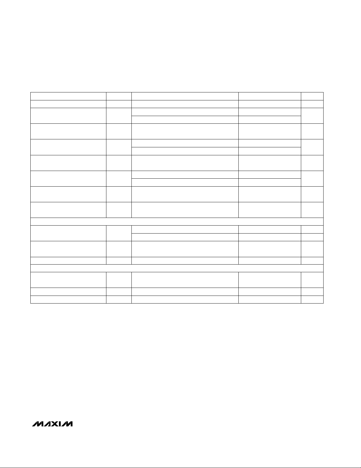
Ordering Information
Selector Guide
Note: There is a minimum order increment of 2500 pieces for
SOT23 packages.
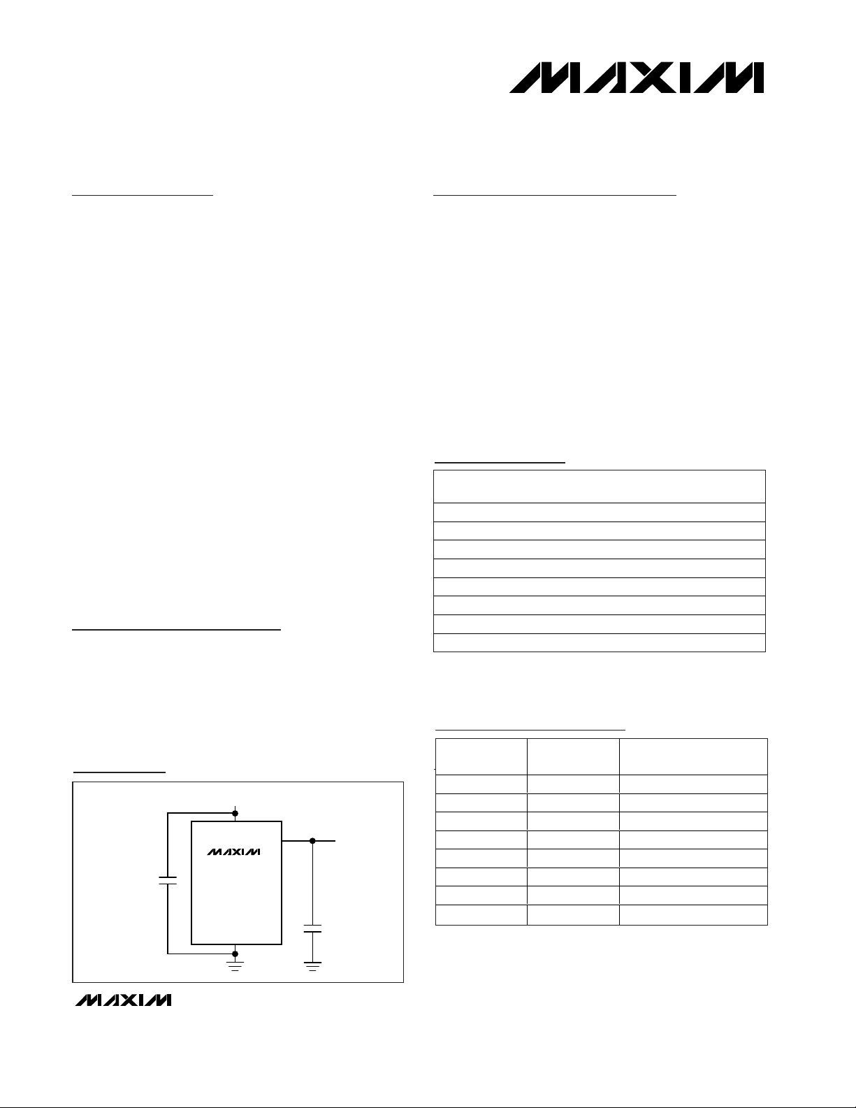
IN
+SUPPLY INPUT (SEE
SELECTOR GUIDE
)
OUT REFERENCE
OUT
1µF*
*CAPACITORS ARE OPTIONAL.
GND
MAX6100–MAX6107
*
Typical Operating Circuit
PART
TEMP RANGE
PIN-
TOP
MARK
MAX6100EUR-T
3 SOT23-3
FZID
MAX6101EUR-T
3 SOT23-3
FZGT
MAX6102EUR-T
3 SOT23-3
FZGU
MAX6103EUR-T
3 SOT23-3
FZGV
MAX6104EUR-T
3 SOT23-3
FZGW
MAX6105EUR-T
3 SOT23-3
FZGX
MAX6106EUR-T
3 SOT23-3
FZJR
MAX6107EUR-T
3 SOT23-3
FZMV
For pricing, delivery, and ordering information, please contact Maxim/Dallas Direct! at
1-888-629-4642, or visit Maxim’s website at www.maxim-ic.com.
Pin Configuration appears at end of data sheet.
PACKAGE
-40°C to +85°C
-40°C to +85°C
-40°C to +85°C
-40°C to +85°C
-40°C to +85°C
-40°C to +85°C
-40°C to +85°C
-40°C to +85°C
OUTPUT
PART
MAX6100 1.800 2.5 to 12.6
MAX6101 1.250 2.5 to 12.6
MAX6102 2.500 (V
MAX6103 3.000 (V
MAX6104 4.096 (V
MAX6105 5.000 (V
MAX6106 2.048 2.5 to 12.6
MAX6107 4.5 (V
VOLTAGE (V)
INPUT VOLTAGE
RANGE (V)
+ 200mV) to 12.6
OUT
+ 200mV) to 12.6
OUT
+ 200mV) to 12.6
OUT
+ 200mV) to 12.6
OUT
+ 200mV) to 12.6
OUT
Page 2
MAX6100–MAX6107
Low-Cost, Micropower, Low-Dropout,
High-Output-Current, SOT23 Voltage References
2 _______________________________________________________________________________________
ABSOLUTE MAXIMUM RATINGS
ELECTRICAL CHARACTERISTICS—MAX6101, V
OUT
= 1.25V
(VIN= 5V, I
OUT
= 0, TA= T
MIN
to T
MAX
, unless otherwise noted. Typical values are at TA= +25°C.) (Note 1)
Stresses beyond those listed under “Absolute Maximum Ratings” may cause permanent damage to the device. These are stress ratings only, and functional
operation of the device at these or any other conditions beyond those indicated in the operational sections of the specifications is not implied. Exposure to
absolute maximum rating conditions for extended periods may affect device reliability.
(Voltages Referenced to GND)
IN .........................................................................-0.3V to +13.5V
OUT .............................................................-0.3V to (VIN+ 0.3V)
Output Short-Circuit to GND or IN (VIN< 6V) ............Continuous
Output Short-Circuit to GND or IN (VIN≥ 6V) .........................60s
Continuous Power Dissipation (TA= +70°C)
3-Pin SOT23 (derate 4.0mW/°C above +70°C)............320mW
Operating Temperature Range ...........................-40°C to +85°C
Storage Temperature Range .............................-65°C to +150°C
Lead Temperature (soldering, 10s) .................................+300°C
-40°C to +85°C
2.5V ≤ VIN≤ 12.6V
0°C to +70°C
TA= +25°C
Guaranteed by line-regulation test
To V
OUT
= 0.1% of final value, C
OUT
= 50pF
VIN= 5V ±100mV, f = 120Hz
1000hr at +25°C
Short to IN
2.5V ≤ VIN≤ 12.6V
Sourcing: 0 ≤ I
OUT
≤ 5mA
Sinking: -2mA ≤ I
OUT
≤ 0
f = 10Hz to 10kHz
Short to GND
f = 0.1Hz to 10Hz
CONDITIONS
µA/V
48
IIN/V
IN
Change in Supply Current
µA
90 125
I
IN
Quiescent Supply Current
V
2.5 12.6
V
IN
Supply Voltage Range
µs
50
t
R
Turn-On Settling Time
dB
86
∆V
OUT
/
∆V
IN
Ripple Rejection
µV
RMS
15
µV
P-P
13
e
OUT
Noise Voltage
75
ppm/°C
65
TCV
OUT
V
1.245 1.250 1.255
V
OUT
Output Voltage
Output Voltage Temperature
Coefficient (Notes 2, 3)
ppm
130
∆V
OUT
/
cycle
Output Voltage Hysteresis
(Note 4)
ppm/
1000hr
50
∆V
OUT
/
time
Long-Term Stability
12
µV/V
90
∆V
OUT
/
∆V
IN
Line Regulation
mV/mA
0.9
∆V
OUT
/
∆I
OUT
Load Regulation
3.0
mA
110
I
SC
OUT Short-Circuit Current
UNITSMIN TYP MAXSYMBOLPARAMETER
DYNAMIC CHARACTERISTICS
INPUT CHARACTERISTICS
Page 3
MAX6100–MAX6107
Low-Cost, Micropower, Low-Dropout,
High-Output-Current, SOT23 Voltage References
_______________________________________________________________________________________ 3
ELECTRICAL CHARACTERISTICS—MAX6100, V
OUT
= 1.8V
(VIN= 5V, TA= T
MIN
to T
MAX
, unless otherwise noted. Typical values are at TA= +25°C) (Note 1)
PARAMETER
SYMBOL
CONDITIONS
MIN
TYP
MAX
UNITS
Output Voltage
V
0°C to +70°C
65
Output Voltage Temperature
Coefficient (Notes 2, 3)
-40°C to +85°C75
ppm/°C
Line Regulation
∆V
IN
2.5V ≤ VIN ≥ 12.6V
µV/V
Sourcing: 0 ≤ I
OUT
≤ 5mA
0.9
Load Regulation
Sinking: -2mA ≤ I
OUT
≤ 0
4.0
mV/mA
Short to GND
OUT Short-Circuit Current
I
SC
Short to IN 12
mA
Long-Term Stability
time
1000hr at +25°C50
ppm/
1000hr
Output Voltage Hysteresis
(Note 4)
cycle
ppm
DYNAMIC CHARACTERISTICS
f = 0.1Hz to 10Hz
22 µV
P-P
Noise Voltage
e
OUT
f = 10Hz to 10kHz
25
µV
RMS
Ripple Rejection
∆V
IN
V
IN
= 5V, ±100mV, f = 120Hz
86 dB
Turn-On Settling Time
t
R
To V
OUT
= 0.1% of final value,
C
OUT
= 50pF
µs
INPUT CHARACTERISTICS
Supply Voltage Range
V
IN
Guaranteed by line-regulation test
2.5
V
Quiescent Supply Current
I
IN
90
µA
Change in Supply Current
2.5V ≤ VIN ≤ 12.6V 4 8 µA/V
V
TCV
∆V
∆V
∆I
∆V
∆V
∆V
OUT
OUT
OUT
OUT
OUT
OUT
OUT
TA = +25°C
OUT
/
/
/
/
/
1.793 1.800 1.807
200
110
130
100
12.6
IIN/V
125
Page 4
ELECTRICAL CHARACTERISTICS—MAX6106, V
OUT
= 2.048V
(VIN= 5V, I
OUT
= 0, TA= T
MIN
to T
MAX
, unless otherwise noted. Typical values are at TA= +25°C.) (Note 1)
MAX6100–MAX6107
Low-Cost, Micropower, Low-Dropout,
High-Output-Current, SOT23 Voltage References
4 _______________________________________________________________________________________
PARAMETER
CONDITIONS MIN
UNITS
Output Voltage V
OUT
TA = +25°C
V
0°C to +70°C65Output Voltage Temperature
Coefficient (Notes 2, 3)
-40°C to +85°C75
ppm/°C
Line Regulation
∆V
IN
_
2.5V ≤ VIN ≥ 12.6V
µV/V
Sourcing : 0 ≤ I
OUT
≤ 5mA
Load Regulation
Sinking: -2mA ≤ I
OUT
≤ 0
mV/mA
Short to GND 110
OUT Short-Circuit Current I
SC
Short to IN 12
mA
Long-Term Stability
time
1000hr at +25°C50
ppm/
1000hr
Output Voltage Hysteresis
(Note 4)
cycle
130 ppm
f= 0.1Hz to 10Hz 22 µV
P-P
Noise Voltage e
OUT
f= 10Hz to 10kHz 25
µV
RMS
Ripple Rejection
∆V
IN
VIN = 5V ±100mV, f = 120Hz 86 dB
Turn-On Settling Time t
R
To V
OUT
= 0.1% of final value,
C
OUT
= 50pF
100 µs
INPUT CHARACTERISTICS
Supply Voltage Range V
IN
Guaranteed by line-regulation test 2.5
V
Quiescent Supply Current I
IN
90
µA
Change in Supply Current
2.5 ≤ VIN ≤ 12.6V 4 8 µA/V
DYNAMIC CHARACTERISTICS
SYMBOL
TCV
OUT
∆V
/
OUT
∆V
/
OUT
∆I
OUT
∆V
/
OUT
∆V
/
OUT
∆V
/
OUT
IIN / V
IN
TYP MAX
2.040 2.048 2.056
200
0.9
4.0
12.6
125
Page 5
MAX6100–MAX6107
Low-Cost, Micropower, Low-Dropout,
High-Output-Current, SOT23 Voltage References
_______________________________________________________________________________________ 5
ELECTRICAL CHARACTERISTICS—MAX6102, V
OUT
= 2.50V
(VIN= 5V, I
OUT
= 0, TA= T
MIN
to T
MAX
, unless otherwise noted. Typical values are at TA= +25°C.) (Note 1)
-40°C to +85°C
(V
OUT
+ 0.2V) ≤ VIN≤ 12.6V
0°C to +70°C
TA= +25°C
Guaranteed by line-regulation test
To V
OUT
= 0.1% of final value, C
OUT
= 50pF
VIN= 5V ±100mV, f = 120Hz
1000hr at +25°C
Short to IN
(V
OUT
+ 0.2V) ≤ VIN≤ 12.6V
Sourcing: 0 ≤ I
OUT
≤ 5mA
Sinking: -2mA ≤ I
OUT
≤ 0
f = 10Hz to 10kHz
Short to GND
f = 0.1Hz to 10Hz
CONDITIONS
µA/V
48
IIN/V
IN
Change in Supply Current
µA
90 125
I
IN
Quiescent Supply Current
V
V
OUT
+
12.6
0.2
V
IN
Supply Voltage Range
µs
115
t
R
Turn-On Settling Time
dB
86
∆V
OUT
/
∆V
IN
Ripple Rejection
µV
RMS
30
µV
P-P
27
e
OUT
Noise Voltage
75
ppm/°C
65
TCV
OUT
V
2.490 2.50 2.510
V
OUT
Output Voltage
Output Voltage Temperature
Coefficient (Notes 2, 3)
ppm
130
∆V
OUT
/
cycle
Output Voltage Hysteresis
(Note 4)
ppm/
1000hr
50
∆V
OUT
/
time
Long-Term Stability
12
µV/V
300
∆V
OUT
/
∆V
IN
Line Regulation
mV/mA
0.9
∆V
OUT
/
∆I
OUT
Load Regulation
5.0
mA
110
I
SC
OUT Short-Circuit Current
UNITSMIN TYP MAXSYMBOLPARAMETER
I
OUT
= 1mA mV
50 200
V
IN
-
V
OUT
Dropout Voltage (Note 5)
DYNAMIC CHARACTERISTICS
INPUT CHARACTERISTICS
Page 6

MAX6100–MAX6107
Low-Cost, Micropower, Low-Dropout,
High-Output-Current, SOT23 Voltage References
6 _______________________________________________________________________________________
ELECTRICAL CHARACTERISTICS—MAX6103, V
OUT
= 3.0V
(VIN= 5V, I
OUT
= 0, TA= T
MIN
to T
MAX
, unless otherwise noted. Typical values are at TA= +25°C.) (Note 1)
I
OUT
= 1mA mV
-40°C to +85°C
50 200
(V
OUT
+ 0.2V) ≤ VIN≤ 12.6V
0°C to +70°C
TA= +25°C
Guaranteed by line-regulation test
To V
OUT
= 0.1% of final value, C
OUT
= 50pF
VIN= 5V ±100mV, f = 120Hz
1000hr at +25°C
Short to IN
(V
OUT
+ 0.2V) ≤ VIN≤ 12.6V
Sourcing: 0 ≤ I
OUT
≤ 5mA
Sinking: -2mA ≤ I
OUT
≤ 0
f = 10Hz to 10kHz
Short to GND
f = 0.1Hz to 10Hz
CONDITIONS
V
IN
-
V
OUT
Dropout Voltage (Note 5)
µA/V
48
IIN/V
IN
Change in Supply Current
µA
90 125
I
IN
Quiescent Supply Current
V
V
OUT
+
12.6
0.2
V
IN
Supply Voltage Range
µs
115
t
R
Turn-On Settling Time
dB
76
∆V
OUT
/
∆V
IN
Ripple Rejection
µV
RMS
40
µV
P-P
35
e
OUT
Noise Voltage
75
ppm/°C
65
TCV
OUT
V
2.988 3.000 3.012
V
OUT
Output Voltage
Output Voltage Temperature
Coefficient (Notes 2, 3)
ppm
130
∆V
OUT
/
cycle
Output Voltage Hysteresis
(Note 4)
ppm/
1000hr
50
∆V
OUT
/
time
Long-Term Stability
12
µV/V
400
∆V
OUT
/
∆V
IN
Line Regulation
mV/mA
0.9
∆V
OUT
/
∆I
OUT
Load Regulation
6.0
mA
110
I
SC
OUT Short-Circuit Current
UNITSMIN TYP MAXSYMBOLPARAMETER
DYNAMIC CHARACTERISTICS
INPUT CHARACTERISTICS
Page 7

MAX6100–MAX6107
Low-Cost, Micropower, Low-Dropout,
High-Output-Current, SOT23 Voltage References
_______________________________________________________________________________________ 7
ELECTRICAL CHARACTERISTICS—MAX6104, V
OUT
= 4.096V
(VIN= 5V, I
OUT
= 0, TA= T
MIN
to T
MAX
, unless otherwise noted. Typical values are at TA= +25°C.) (Note 1)
I
OUT
= 1mA mV
-40°C to +85°C
50 200
(V
OUT
+ 0.2V) ≤ VIN≤ 12.6V
0°C to +70°C
TA= +25°C
Guaranteed by line-regulation test
To V
OUT
= 0.1% of final value, C
OUT
= 50pF
VIN= 5V ±100mV, f = 120Hz
1000hr at +25°C
Short to IN
(V
OUT
+ 0.2V) ≤ VIN≤ 12.6V
Sourcing: 0 ≤ I
OUT
≤ 5mA
Sinking: -2mA ≤ I
OUT
≤ 0
f = 10Hz to 10kHz
Short to GND
f = 0.1Hz to 10Hz
CONDITIONS
V
IN
-
V
OUT
Dropout Voltage (Note 5)
µA/V
48
IIN/V
IN
Change in Supply Current
µA
90 125
I
IN
Quiescent Supply Current
V
V
OUT
+
12.6
0.2
V
IN
Supply Voltage Range
µs
190
t
R
Turn-On Settling Time
dB
72
∆V
OUT
/
∆V
IN
Ripple Rejection
µV
RMS
50
µV
P-P
50
e
OUT
Noise Voltage
75
ppm/°C
65
TCV
OUT
V
4.080 4.096 4.112
V
OUT
Output Voltage
Output Voltage Temperature
Coefficient (Notes 2, 3)
ppm
130
∆V
OUT
/
cycle
Output Voltage Hysteresis
(Note 4)
ppm/
1000hr
50
∆V
OUT
/
time
Long-Term Stability
12
µV/V
430
∆V
OUT
/
∆V
IN
Line Regulation
mV/mA
0.9
∆V
OUT
/
∆I
OUT
Load Regulation
8.0
mA
110
I
SC
OUT Short-Circuit Current
UNITSMIN TYP MAXSYMBOLPARAMETER
DYNAMIC CHARACTERISTICS
INPUT CHARACTERISTICS
Page 8

MAX6100–MAX6107
Low-Cost, Micropower, Low-Dropout,
High-Output-Current, SOT23 Voltage References
8 _______________________________________________________________________________________
ELECTRICAL CHARACTERISTICS—MAX6107, V
OUT
= 4.5V
(VIN= 5V, I
OUT
= 0, TA= T
MIN
to T
MAX
, unless otherwise noted. Typical values are at TA= +25°C.) (Note 1)
I
OUT
= 1mA mV
-40°C to +85°C
50 200
(V
OUT
+ 0.2V) ≤ VIN≤ 12.6V
0°C to +70°C
TA= +25°C
Guaranteed by line-regulation test
To V
OUT
= 0.1% of final value, C
OUT
= 50pF
VIN= 5V ±100mV, f = 120Hz
1000hr at +25°C
Short to IN
(V
OUT
+ 0.2V) ≤ VIN≤ 12.6V
Sourcing: 0 ≤ I
OUT
≤ 5mA
Sinking: -2mA ≤ I
OUT
≤ 0
f = 10Hz to 10kHz
Short to GND
f = 0.1Hz to 10Hz
CONDITIONS
V
IN
-
V
OUT
Dropout Voltage (Note 5)
µA/V
48
IIN/V
IN
Change in Supply Current
µA
90 125
I
IN
Quiescent Supply Current
V
V
OUT
+
12.6
0.2
V
IN
Supply Voltage Range
µs
230
t
R
Turn-On Settling Time
dB
70
∆V
OUT
/
∆V
IN
Ripple Rejection
µV
RMS
55
µV
P-P
55
e
OUT
Noise Voltage
75
ppm/°C
65
TCV
OUT
V
4.482 4.500 4.518
V
OUT
Output Voltage
Output Voltage Temperature
Coefficient (Notes 2, 3)
ppm
130
∆V
OUT
/
cycle
Output Voltage Hysteresis
(Note 4)
ppm/
1000hr
50
∆V
OUT
/
time
Long-Term Stability
12
µV/V
550
∆V
OUT
/
∆V
IN
Line Regulation
mV/mA
0.9
∆V
OUT
/
∆I
OUT
Load Regulation
8.0
mA
110
I
SC
OUT Short-Circuit Current
UNITSMIN TYP MAXSYMBOLPARAMETER
DYNAMIC CHARACTERISTICS
INPUT CHARACTERISTICS
Page 9

MAX6100–MAX6107
Low-Cost, Micropower, Low-Dropout,
High-Output-Current, SOT23 Voltage References
_______________________________________________________________________________________ 9
Note 1: Devices are 100% production tested at TA= +25°C and are guaranteed by design from TA= T
MIN
to T
MAX
by correlation to
sample units characterized over temperature.
Note 2: Temperature coefficient is specified by the “box” method, i.e., the maximum ∆V
OUT
is divided by the maximum ∆t.
Note 3: Not production tested. Guaranteed by design.
Note 4: Thermal hysteresis is defined as the change in +25°C output voltage before and after temperature cycling of the device
from T
A
= T
MIN
to T
MAX
.
Note 5: Dropout voltage is the minimum input voltage at which V
OUT
changes ≤ 0.2% from V
OUT
at VIN= 5.0V (VIN= 5.5V for
MAX6105).
ELECTRICAL CHARACTERISTICS—MAX6105, V
OUT
= 5.000V
(VIN= 5.5V, I
OUT
= 0, TA= T
MIN
to T
MAX
, unless otherwise noted. Typical values are at TA= +25°C.) (Note 1)
I
OUT
= 1mA mV
-40°C to +85°C
50 200
(V
OUT
+ 0.2V) ≤ VIN≤ 12.6V
0°C to +70°C
TA= +25°C
Guaranteed by line-regulation test
To V
OUT
= 0.1% of final value, C
OUT
= 50pF
VIN= 6V ±100mV, f = 120Hz
1000hr at +25°C
Short to IN
(V
OUT
+ 0.2V) ≤ VIN≤ 12.6V
Sourcing: 0 ≤ I
OUT
≤ 5mA
Sinking: -2mA ≤ I
OUT
≤ 0
f = 10Hz to 10kHz
Short to GND
f = 0.1Hz to 10Hz
CONDITIONS
V
IN
-
V
OUT
Dropout Voltage (Note 5)
µA/V
48
IIN/V
IN
Change in Supply Current
µA
90 125
I
IN
Quiescent Supply Current
V
V
OUT
+
12.6
0.2
V
IN
Supply Voltage Range
µs
300
t
R
Turn-On Settling Time
dB
65
∆V
OUT
/
∆V
IN
Ripple Rejection
µV
RMS
60
µV
P-P
60
e
OUT
Noise Voltage
75
ppm/°C
65
TCV
OUT
V
4.980 5.000 5.020
V
OUT
Output Voltage
Output Voltage Temperature
Coefficient (Notes 2, 3)
ppm
130
∆V
OUT
/
cycle
Output Voltage Hysteresis
(Note 4)
ppm/
1000hr
50
∆V
OUT
/
time
Long-Term Stability
12
µV/V
550
∆V
OUT
/
∆V
IN
Line Regulation
mV/mA
0.9
∆V
OUT
/
∆I
OUT
Load Regulation
10
mA
110
I
SC
OUT Short-Circuit Current
UNITSMIN TYP MAXSYMBOLPARAMETER
DYNAMIC CHARACTERISTICS
INPUT CHARACTERISTICS
Page 10

MAX6100–MAX6107
Low-Cost, Micropower, Low-Dropout,
High-Output-Current, SOT23 Voltage References
10 ______________________________________________________________________________________
Typical Operating Characteristics
(TA = +25°C, unless otherwise noted.)
Typical Operating Characteristics
(TA = +25°C, unless otherwise noted.)
2.488
2.491
2.490
2.489
2.493
2.492
2.497
2.496
2.495
2.494
-40 -20 0 20 40 60 80
MAX6102
OUTPUT VOLTAGE TEMPERATURE DRIFT
MAX6100/07 TOC01
TEMPERATURE (°C)
OUTPUT VOLTAGE (V)
3 TYPICAL PARTS
TEMPERATURE RISING
4.990
4.996
4.994
4.992
5.000
4.998
5.004
5.002
-40 -20 0 20 40 60 80
MAX6105
OUTPUT VOLTAGE TEMPERATURE DRIFT
MAX6100/07 TOC02
TEMPERATURE (°C)
OUTPUT VOLTAGE (V)
3 TYPICAL PARTS
TEMPERATURE RISING
0
40
20
80
60
100
120
28104 6 12 14
SUPPLY CURRENT
vs. INPUT VOLTAGE
MAX6100/07 TOC03
INPUT VOLTAGE (V)
SUPPLY CURRENT (µA)
70
80
90
100
110
120
-40 10-15 35 60 85
MAX6100/07 toc04
TEMPERATURE (°C)
SUPPLY CURRENT (µA)
MAX6101
SUPPLY CURRENT vs. TEMPERATURE
VIN = 12.5V
VIN = 7.5V
VIN = 2.5V
VIN = 5.5V
0
50
150
100
200
250
012345
MAX6102
DROPOUT VOLTAGE vs. SOURCE CURRENT
MAX6100/07 TOC05
SOURCE CURRENT (mA)
DROPOUT VOLTAGE (mV)
TA = +85°C
TA = +25°C
TA = -40°C
-90
-70
-30
-50
-10
-80
-40
-60
-20
0
0 0.5 1.0 1.5 2.0 2.5
MAX6102
DROPOUT VOLTAGE vs. SINK CURRENT
MAX6100/07 TOC06
SINK CURRENT (mA)
DROPOUT VOLTAGE (mV)
TA = +85°C
TA = +25°C
TA = -40°C
0
50
150
100
200
250
021 3456
MAX6105
DROPOUT VOLTAGE vs. SOURCE CURRENT
MAX6100/07 TOC07
SOURCE CURRENT (mA)
DROPOUT VOLTAGE (mV)
TA = +85°C
TA = +25°C
TA = -40°C
-90
-70
-30
-50
-10
-80
-40
-60
-20
0
0 0.5 1.0 1.5 2.0 2.5
MAX6105
DROPOUT VOLTAGE vs. SINK CURRENT
MAX6100/07 TOC08
SINK CURRENT (mA)
DROPOUT VOLTAGE (mV)
TA = +85°C
TA = +25°C
TA = -40°C
-2
0
-1
2
1
4
3
5
7
6
8
-6 -2 0 2-4 4 6 8 10 12
MAX6102
LOAD REGULATION
MAX6100/07 TOC09
LOAD CURRENT (mA)
OUTPUT VOLTAGE CHANGE (mV)
TA = +85°C
TA = +85°C
TA = +25°C
TA = +25°C
TA = -40°C
TA = -40°C
SOURCE
SINK
Page 11

Typical Operating Characteristics (continued)
(TA = +25°C, unless otherwise noted.)
MAX6100–MAX6107
Low-Cost, Micropower, Low-Dropout,
High-Output-Current, SOT23 Voltage References
______________________________________________________________________________________ 11
-1
0
2
1
4
3
5
-6 -2 0 2-4 4 6 8 10 12
MAX6105
LOAD REGULATION
MAX6100/07 TOC10
LOAD CURRENT (mA)
OUTPUT VOLTAGE CHANGE (mV)
TA = +85°C
TA = +85°C
TA = +25°C
TA = +25°C
TA = -40°C
TA = -40°C
SINK SOURCE
-0.10
0
-0.05
0.10
0.05
0.20
0.15
0.25
2684101214
MAX6102
LINE REGULATION
MAX6100/07 TOC11
INPUT VOLTAGE (V)
OUTPUT VOLTAGE CHANGE (mV)
TA = +85°C
TA = +25°C
TA = -40°C
-0.05
0.15
0
0.25
0.20
0.35
0.30
0.40
468101214
MAX6105
LINE REGULATION
MAX6100/07 TOC12
INPUT VOLTAGE (V)
OUTPUT VOLTAGE CHANGE (mV)
0.05
0.10
TA = +85°C
TA = +25°C
TA = -40°C
100
90
80
70
60
50
40
30
20
0
0.001 1 10 1000.01 0.1 1000
MAX6102
POWER-SUPPLY REJECTION RATIO
vs. FREQUENCY
10
MAX6100/07 TOC13
FREQUENCY (kHz)
PSRR (dB)
80
70
60
50
40
30
20
0
0.001 1 10 1000.01 0.1 1000
MAX6105
POWER-SUPPLY REJECTION RATIO
vs. FREQUENCY
10
MAX6100/07 TOC14
FREQUENCY (kHz)
PSRR (dB)
MAX6101
LINE-TRANSIENT RESPONSE
MAX6100/07 TOC15
100µs/div
V
IN
200mV/div
V
OUT
200mV/div
MAX6102
LINE-TRANSIENT RESPONSE
MAX6100/07 TOC16
100µs/div
V
IN
200mV/div
V
OUT
100mV/div
MAX6105
LINE-TRANSIENT RESPONSE
MAX6100/07 TOC17
100µs/div
V
IN
200mV/div
V
OUT
5mV/div
0.01 100 10k10.1 10 1k 100k 1M
OUTPUT IMPEDANCE vs. FREQUENCY
MAX6100/07 TOC18
FREQUENCY (Hz)
OUTPUT IMPEDANCE (Ω)
-100
100
0
300
200
400
600
700
500
800
Page 12

Typical Operating Characteristics (continued)
(TA = +25°C, unless otherwise noted.)
MAX6100–MAX6107
Low-Cost, Micropower, Low-Dropout,
High-Output-Current, SOT23 Voltage References
12 ______________________________________________________________________________________
MAX6105
LOAD-TRANSIENT RESPONSE (C
LOAD
= 0)
MAX6100/07 TOC21
200µs/div
5mA
-2mA
V
OUT
200mV/div
I
OUT
5mA/div
MAX6102
LOAD-TRANSIENT RESPONSE (C
LOAD
= 1µF)
MAX6100/07 TOC22
200µs/div
V
IN
2V/div
V
OUT
50mV/div
MAX6105
LOAD-TRANSIENT RESPONSE (C
LOAD
= 1µF)
MAX6100/07 TOC23
100µs/div
V
IN
5V/div
V
OUT
50mV/div
MAX6101
TURN-ON TRANSIENT
MAX6100/07 TOC24
100µs/div
V
IN
2V/div
V
OUT
500mV/div
MAX6101
LOAD-TRANSIENT RESPONSE (C
LOAD
= 0)
MAX6100/07 TOC19
200µs/div
4mA
-2mA
V
OUT
200mV/div
I
OUT
5mA/div
MAX6102
LOAD-TRANSIENT RESPONSE (C
LOAD
= 0)
MAX6100/07 TOC20
200µs/div
5mA
-2mA
V
OUT
200mV/div
I
OUT
5mA/div
Page 13

MAX6100–MAX6107
Low-Cost, Micropower, Low-Dropout,
High-Output-Current, SOT23 Voltage References
______________________________________________________________________________________ 13
Applications Information
Input Bypassing
For the best line-transient performance, decouple the
input with a 0.1µF ceramic capacitor as shown in the
Typical Operating Circuit. Locate the capacitor as close
to IN as possible. Where transient performance is less
important, no capacitor is necessary.
Output/Load Capacitance
Devices in the MAX6100 family do not require an output
capacitance for frequency stability. They are stable for
any capacitive load when sourcing less than 200µA.
When sourcing greater than 200µA, the output may
become unstable with capacitive loads between 0.5nF
and 50nF. In applications where the load or the supply
can experience step changes, an output capacitor
reduces the amount of overshoot (undershoot) and
improves the circuit’s transient response. Many applications do not require an external capacitor, and the
MAX6100 family can offer a significant advantage in
these applications when board space is critical.
Supply Current
The quiescent supply current of the series-mode
MAX6100 family is typically 90µA and is virtually independent of the supply voltage, with only an 8µA/V (max) variation with supply voltage. Unlike series references,
shunt-mode references operate with a series resistor connected to the power supply. The quiescent current of a
shunt-mode reference is thus a function of the input voltage. Additionally, shunt-mode references have to be
biased at the maximum-expected load current, even if the
load current is not present at the time. In the MAX6100
family, the load current is drawn from the input voltage
only when required, so supply current is not wasted and
efficiency is maximized at all input voltages. This
improved efficiency reduces power dissipation and
extends battery life. When the supply voltage is below the
minimum specified input voltage (as during turn-on), the
devices can draw up to 400µA beyond the nominal
supply current. The input voltage source must be capable
of providing this current to ensure reliable turn-on.
Output Voltage Hysteresis
Output voltage hysteresis is the change of output voltage
at T
A
= +25°C before and after the device is cycled
over its entire operating temperature range. Hysteresis
is caused by differential package stress appearing
across the bandgap core transistors. The typical temperature hysteresis value is 130ppm.
Typical Operating Characteristics (continued)
(TA= +25°C, unless otherwise noted.)
NAME FUNCTION
1 IN Input Voltage
2 OUT Reference Output
PIN
3 GND Ground
Pin Description
MAX6105
TURN-ON TRANSIENT
MAX6100/07 TOC25
100µs/div
V
IN
2V/div
V
OUT
2V/div
MAX6102
0.1Hz TO 10Hz OUTPUT NOISE
MAX6100/07 TOC26
1s/div
20µV/div
MAX6105
0.1Hz TO 10Hz OUTPUT NOISE
MAX6100/07 TOC27
1s/div
20µV/div
Page 14

MAX6100–MAX6107
Low-Cost, Micropower, Low-Dropout,
High-Output-Current, SOT23 Voltage References
Maxim cannot assume responsibility for use of any circuitry other than circuitry entirely embodied in a Maxim product. No circuit patent licenses are
implied. Maxim reserves the right to change the circuitry and specifications without notice at any time.
14 ____________________Maxim Integrated Products, 120 San Gabriel Drive, Sunnyvale, CA 94086 408-737-7600
© 2002 Maxim Integrated Products Printed USA is a registered trademark of Maxim Integrated Products.
SOTPO3L.EPS
Turn-On Time
These devices typically turn on and settle to within 0.1%
of their final value in 50µs to 300µs. The turn-on time can
increase up to 1.5ms with the device operating at the
minimum dropout voltage and the maximum load.
Chip Information
TRANSISTOR COUNT: 117
OUT
1
3 GND
IN
SOT23
TOP VIEW
2
MAX6100–MAX6107
Pin Configuration
Package Information
(The package drawing(s) in this data sheet may not reflect the most current specifications. For the latest package outline information,
go to www.maxim-ic.com/packages.)
 Loading...