Maxim MAX607EUA, MAX607ESA, MAX606EUA, MAX606ESA Datasheet

General Description
The MAX606/MAX607 are the smallest CMOS, step-up
DC-DC converters available for flash memory and PC
(PCMCIA) cards. They switch at up to 1MHz, permitting
the entire circuit to fit in 0.25in2, yet remain under
1.35mm high to fit Type 1, 2, and 3 card standards.
These devices operate from a 3V to 5.5V input and provide a ±4% accurate output that is preset to 5V or 12V,
or adjustable from VINto 12.5V. They can provide up to
180mA of output current at 5V.
The MAX606 switches at up to 1MHz and fits Type 1
(thinnest standard) flash memory and PCMCIA cards. It
uses a thin, 1.19mm high, 5µH inductor and small,
0.68µF output capacitors. The entire circuit fits in
0.25in2and is less than 1.35mm high.
The MAX607 switches at up to 500kHz, fitting Type 2
and 3 cards, as well as hand-held devices where
height requirements are not as critical. It uses less
board area than the MAX606, fitting in 0.16in2, but
requires 2.5mm of height. It also has a lower no-load
supply current than the MAX606.
Both devices use a unique control scheme that optimizes
efficiency over all input and output voltages. Other features include 1µA logic-controlled shutdown and usercontrolled soft-start to minimize inrush currents.
The MAX606/MAX607 come in 8-pin µMAX and SO
packages. The µMAX package uses half the board
area of a standard 8-pin SO and has a maximum height
of just 1.11mm.
________________________Applications
PCMCIA Cards
Memory Cards
Single PCMCIA Slot Programming
Digital Cameras
Flash Memory Programming
Hand-Held Equipment
____________________________Features
♦ Lowest-Height Circuit (1.35mm max)
♦ ±4% Regulated Output (5V, 12V, or Adjustable)
♦ Up to 180mA Load Current
♦ 1MHz Switching Frequency (MAX606)
♦ 1µA Logic-Controlled Shutdown
♦ 3V to 5.5V Input Voltage Range
♦ Compact 8-Pin µMAX Package
MAX606/MAX607
Low-Profile, 5V/12V or Adjustable, Step-Up
DC-DC Converters for Flash Memory/PCMCIA Cards
________________________________________________________________
Maxim Integrated Products
1
1
2
3
4
8
7
6
5
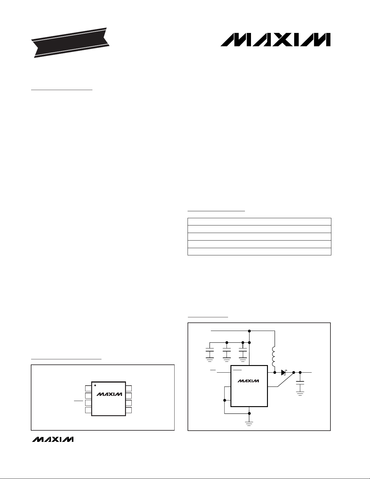
LX
OUT
SS
GND
PGND
FB
SHDN
IN
MAX606
MAX607
SO/µMAX
TOP VIEW
Pin Configuration
0.68µF 0.68µF
0.68µF
x 2
0.1µF
5µH
MAX606
LX
OUT
SHDN
FB
GND
PGND
IN
ON/OFF
OUTPUT
12V @ 90mA
INPUT
+4.5V TO +5.5V
Typical Operating Circuit
19-0459; Rev 1; 1/99
EVALUATION KIT MANUAL
FOLLOWS DATA SHEET
Ordering Information
For free samples & the latest literature: http://www.maxim-ic.com, or phone 1-800-998-8800.
For small orders, phone 1-800-835-8769.
MAX607EUA -40°C to +85°C 8 µMAX
MAX607ESA -40°C to +85°C 8 SO
MAX606EUA -40°C to +85°C 8 µMAX
MAX606ESA -40°C to +85°C 8 SO
PART TEMP. RANGE PIN-PACKAGE

MAX606/MAX607
Low-Profile, 5V/12V or Adjustable, Step-Up
DC-DC Converters for Flash Memory/PCMCIA Cards
2 _______________________________________________________________________________________
ABSOLUTE MAXIMUM RATINGS
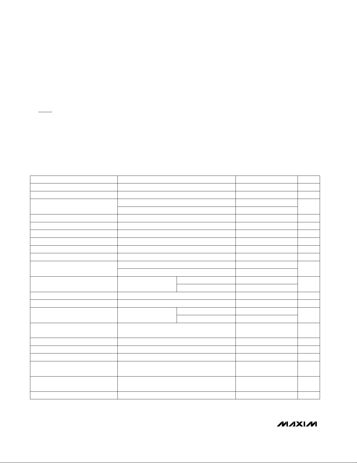
ELECTRICAL CHARACTERISTICS
(VIN= 3.3V, GND = PGND = FB = 0V, SHDN = IN, TA= 0°C to +85°C, unless otherwise noted. Typical values are at TA= +25°C.)
Stresses beyond those listed under “Absolute Maximum Ratings” may cause permanent damage to the device. These are stress ratings only, and functional
operation of the device at these or any other conditions beyond those indicated in the operational sections of the specifications is not implied. Exposure to
absolute maximum rating conditions for extended periods may affect device reliability.
IN to GND.................................................................-0.3V to +6V
LX, OUT to GND.....................................................-0.3V to +15V
PGND to GND.....................................................................±0.3V
FB to GND..................................................-0.3V to (V
CC
+ 0.3V)
SS, SHDN
to GND....................................................-0.3V to +6V
Continuous Power Dissipation (T
A
= +70°C)
µMAX (derate 4.10mW/°C above +70°C) ....................330mW
SO (derate 5.88mW/°C above +70°C).........................471mW
Operating Temperature Range ...........................-40°C to +85°C
Storage Temperature.......................................................+160°C
Lead Temperature (soldering, 10sec).............................+300°C
VIN= 3V to 5.5V. For VFBbelow this voltage,
output regulates to 12V.
V
SHDN
= 0 or V
IN
3V < VIN< 5V, FB = IN, I
LOAD
= 0 to 180mA
VIN= 5.5V
VIN= 3V
2V < (V
OUT
+ 0.5V - VIN) < 8V (see
Pulse-
Frequency-Modulation Control Scheme
section)
3V < VIN< 5.5V
(tON= K / VIN)
V
OUT
= 13V
V
SHDN
= VIN, VSS= 150mV
V
SHDN
= 0, OUT = IN
VLX= 12V
4.5V < VIN< 5.5V, FB = GND, I
LOAD
= 0 to 120mA
0.1V < VFB< (VIN- 0.1V)
0.1V < VFB< (VIN- 0.1V)
V
OUT
= 13V
VIN= 3V to 5.5V
V
SHDN
= VSS= 0
CONDITIONS
V0.1FB Input Low Voltage
µA±1
SHDN Input Current
V0.66V
IN
SHDN Input High Voltage
V0.25V
IN
SHDN Input Low Voltage
0.3 0.7Switch Off-Time Ratio
3.8 6.0 8.6
µs-A
1.9 3.0 4.3
Switch On-Time Constant (K)
µA80OUT Input Current
µA0.01 10Shutdown Quiescent Current
150 300
µA
250 500
Quiescent Supply Current
0.5
V
4.8 5.0 5.2
Output Voltage (Note 1)
V2.4 2.8
V3.0 5.5Supply Voltage
Undervoltage Lockout Threshold
kΩ
30 45 60
SS Resistance
A0.7 1.1Switch Current Limit
µA10Switch Off-Leakage
Ω
0.4 1Switch On-Resistance
11.5 12.0 12.5
V1.96 2.00 2.04FB Regulation Setpoint
VV
IN
12.5Adjustable Output Voltage Range
%0.5Line Regulation
UNITSMIN TYP MAXPARAMETER
VIN= 3V to 5.5V. For VFBabove this voltage,
output regulates to 5V.
VVIN- 0.1FB Input High Voltage
VFB= 2.05V, V
OUT
= 13V nA200FB Input Current
MAX606
MAX607
MAX606
MAX607

MAX606/MAX607
Low-Profile, 5V/12V or Adjustable, Step-Up
DC-DC Converters for Flash Memory/PCMCIA Cards
_______________________________________________________________________________________ 3
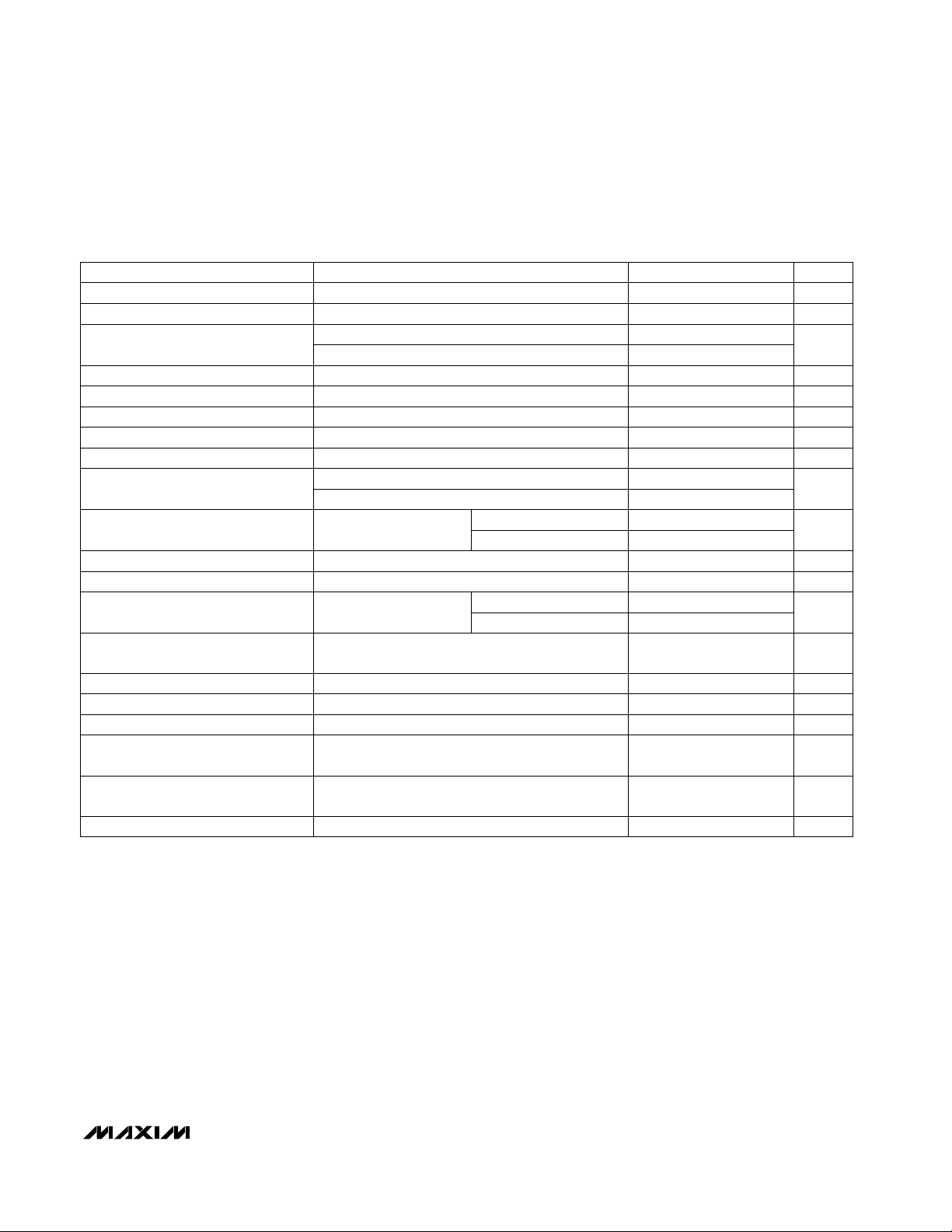
ELECTRICAL CHARACTERISTICS
(VIN= 3.3V, GND = PGND = FB = 0V, SHDN = IN, TA= -40°C to +85°C, unless otherwise noted.) (Note 2)
Note 1: The load specification is guaranteed by DC parametric tests and is not production tested in circuit.
Note 2: Specifications to -40°C are guaranteed by design, not production tested.
VIN= 3V to 5.5V. For VFBbelow this voltage,
output regulates to 12V.
V
SHDN
= 0 or V
IN
3V < VIN< 5V, FB = IN, I
LOAD
= 0 to 135mA
VIN= 5.5V
VIN= 3V
2V < (V
OUT
+ 0.5V - VIN) < 8V (see
Pulse-
Frequency-Modulation Control Scheme
section)
3V < VIN< 5.5V
(tON= K / VIN)
V
OUT
= 13V
V
SHDN
= VIN, VSS= 150mV
V
SHDN
= 0, OUT = IN
MAX606
VLX= 12V
4.5V < VIN< 5.5V, FB = GND, I
LOAD
= 0 to 90mA
0.1V < VFB< (VIN- 0.1V)
0.1V < VFB< (VIN- 0.1V)
V
OUT
= 13V
V
SHDN
= VSS= 0
CONDITIONS
MAX606
V0.1
MAX607
FB Input Low Voltage
µA±1
MAX607
SHDN Input Current
V0.66V
IN
SHDN Input High Voltage
V0.25V
IN
SHDN Input Low Voltage
0.3 0.7Switch Off-Time Ratio
3.5 9.0
µs-V
1.8 4.5
Switch On-Time Constant (K)
µA85OUT Input Current
µA10Shutdown Quiescent Current
300
µA
500
Quiescent Supply Current
0.5
V
4.75 5.25
Output Voltage (Note 1)
V2.4 2.8
V3.0 5.5Supply Voltage
Undervoltage Lockout Threshold
kΩ
30 60
SS Resistance
A0.55 1.25Switch Current Limit
µA10Switch Off-Leakage
Ω
1Switch On-Resistance
11.4 12.6
V1.94 2.06FB Regulation Setpoint
VV
IN
12.5Adjustable Output Voltage Range
UNITSMIN TYP MAXPARAMETER
VIN= 3V to 5.5V. For VFBabove this voltage,
output regulates to 5V.
VVIN- 0.1FB Input High Voltage
VFB= 2.05V, V
OUT
= 13V nA200FB Input Current

MAX606/MAX607
Low-Profile, 5V/12V or Adjustable, Step-Up
DC-DC Converters for Flash Memory/PCMCIA Cards
4 _______________________________________________________________________________________
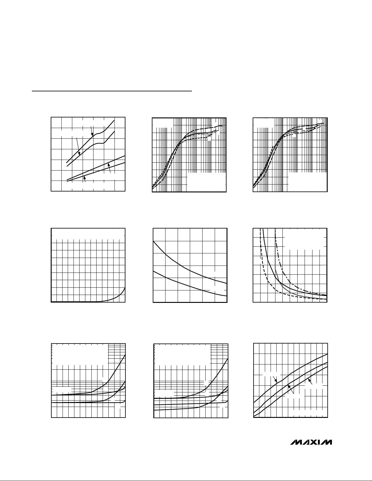
Typical Operating Characteristics
(VIN= 3.3V, TA= +25°C, unless otherwise noted.)
0
200
100
400
300
600
500
700
2.0 3.0 3.52.5 4.0 4.5 5.0 5.5
MAXIMUM OUTPUT CURRENT
vs. INPUT VOLTAGE
MAX606/07toc01
INPUT VOLTAGE (V)
MAXIMUM OUTPUT CURRENT (mA)
MAX606 (V
OUT
= 5V)
MAX607 (V
OUT
= 5V)
MAX606 (V
OUT
= 12V)
MAX607 (V
OUT
= 12V)
0
0.01 1 100 10000.1 10
MAX606
EFFICIENCY vs. OUTPUT CURRENT
20
MAX606/7 TOC02
OUTPUT CURRENT (mA)
EFFICIENCY (%)
40
60
80
10
30
50
70
100
90
A: V
OUT
= 12V, VIN = 3.3V
B: V
OUT
= 5V, VIN = 3.3V
C: V
OUT
= 12V, VIN = 5V
D: V
OUT
= 5V, VIN = 5V
CIN = 2 x 1µF
C
OUT
= 4.7µF
A
C
B
D
0
0.01 1 100 10000.1 10
MAX607
EFFICIENCY vs. OUTPUT CURRENT
20
MAX606/7 TOC03
OUTPUT CURRENT (mA)
EFFICIENCY (%)
40
60
80
10
30
50
70
100
90
A: V
OUT
= 12V, VIN = 3.3V
B: V
OUT
= 5V, VIN = 3.3V
C: V
OUT
= 12V, VIN = 5V
D: V
OUT
= 5V, VIN = 5V
CIN = 2 x 1µF
C
OUT
= 4.7µF
D
B
A
C
0
-40
SHUTDOWN QUIESCENT CURRENT
vs. TEMPERATURE
MAX606/7 TOC04
TEMPERATURE (°C)
SHUTDOWN I
Q
(µA)
0.1
0.2
0.3
0.4
0.5
0.6
0.7
0.8
0.9
1.0
-20 0 20 40 60 80
FOR VIN = 3V, 3.3V, AND 5V
5 MINUTE WAIT BEFORE MEASUREMENT
0
2.5
SWITCH ON-TIME vs.
INPUT VOLTAGE
MAX606/7 TOC-05
INPUT VOLTAGE (V)
SWITCH ON-TIME (ns)
500
1000
1500
2000
2500
3000
3.5 4.5 5.53.0 4.0 5.0
MAX607
MAX606
0
2
SWITCH OFF-TIME vs.
OUTPUT VOLTAGE
MAX606/7 TOC-06
OUTPUT VOLTAGE (V)
SWITCH OFF-TIME (ns)
500
1000
1500
2000
2500
3000
3500
4000
468103 5 7 9 11 12
A: MAX607, VIN = 5V
B: MAX606, V
IN
= 5V
C: MAX607, V
IN
= 3.3V
D: MAX606, V
IN
= 3V
A
B
C D
10,000
100
-40 -20 0 20 40 60 80
MAX607
NO-LOAD SUPPLY CURRENT
vs. TEMPERATURE
MAX606/7-08
TEMPERATURE (˚C)
NO-LOAD SUPPLY CURRENT (µA)
1000
D
B
A
A: V
OUT
= 12V, MBR0520 DIODE
B: V
OUT
= 12V, MBR0540 DIODE
C: V
OUT
= 5V, MBR0520 DIODE
D: V
OUT
= 5V, MBR0540 DIODE
C
VIN = 3.3V
10,000
100
-40 -20 0 20 40 60 80
MAX606
NO-LOAD SUPPLY CURRENT
vs. TEMPERATURE
MAX606/7-07
TEMPERATURE (˚C)
NO-LOAD SUPPLY CURRENT (µA)
1000
D
B
A
A: V
OUT
= 12V, MBR0520 DIODE
B: V
OUT
= 12V, MBR0540 DIODE
C: V
OUT
= 5V, MBR0520 DIODE
D: V
OUT
= 5V, MBR0540 DIODE
C
VIN = 3.3V
10,000
0.001
-40 -20 20
DIODE LEAKAGE CURRENT
vs. TEMPERATURE
0.1
0.01
100
10
1000
MAX606/07-09
TEMPERATURE (°C)
LEAKAGE CURRENT (µA)
040
1
60
80
MBR0520L
MBR0530
MBR0540
V
OUT
= V
ANODE
= 12V
 Loading...