

General Description
The MAX6061–MAX6068 are precision, low-dropout,
micropower voltage references. These three-terminal
devices are available with output voltage options of
1.25V, 1.8V, 2.048V, 2.5V, 3V, 4.096V, 4.5V, and 5V.
They feature a proprietary curvature-correction circuit
and laser-trimmed thin-film resistors that result in a very
low temperature coefficient of 20ppm/°C (max) and an
initial accuracy of ±0.2% (max). Specifications apply to
the extended temperature range (-40°C to +85°C).
The MAX6061–MAX6068 typically draw only 90µA of
supply current and can source 5mA or sink 2mA of load
current. Unlike conventional shunt-mode (two-terminal)
references that waste supply current and require an
external resistor, these devices offer a supply current
that is virtually independent of the supply voltage
(8µA/V variation) and do not require an external resistor. Additionally, the internally compensated devices do
not require an external compensation capacitor.
Eliminating the external compensation capacitor saves
valuable board area in space-critical applications. Low
dropout voltage and supply independent, ultra-low supply current make these devices ideal for battery-operated, high-performance, low-voltage systems.
The MAX6061–MAX6068 are available in a 3-pin SOT23
package.
Applications
Analog-to-Digital Converters (ADCs)
Portable Battery-Powered Systems
Notebook Computers
PDAs, GPSs, DMMs
Cellular Phones
Precision 3V/5V Systems
Features
♦ Ultra-Small 3-Pin SOT23 Package
♦ ±0.2% (max) Initial Accuracy
♦ 20ppm/°C (max) Temperature Coefficient
♦ 5mA Source Current
♦ 2mA Sink Current
♦ No Output Capacitor Required
♦ Stable with Capacitive Loads
♦ 90µA (typ) Quiescent Supply Current
♦ 200mV (max) Dropout at 1mA Load Current
♦ Output Voltage Options: 1.25V, 1.8V, 2.048V, 2.5V,
3V, 4.096V, 4.5V, 5V
♦ 13µVp-p Noise 0.1Hz to 10Hz (MAX6061)
MAX6061–MAX6068
Precision, Micropower, Low-Dropout,
High-Output-Current, SOT23 Voltage References
________________________________________________________________ Maxim Integrated Products 1
19-1659; Rev 1; 4/01
Ordering Information
Pin Configuration
Selector Guide
Note: There is a minimum order increment of 2500 pieces for
SOT23 packages.
Typical Operating Circuit appears at end of data sheet.
PART
OUTPUT
VOLTAGE (V)
INPUT VOLTAGE (V)
MAX6061 1.248 2.5 to 12.6
MAX6062 2.048 2.5 to 12.6
MAX6066 2.500 (V
OUT
+ 200mV) to 12.6
MAX6063 3.000 (V
OUT
+ 200mV) to 12.6
MAX6064 4.096 (V
OUT
+ 200mV) to 12.6
MAX6067 4.500 (V
OUT
+ 200mV) to 12.6
MAX6065 5.000 (V
OUT
+ 200mV) to 12.6
MAX6068 1.800 2.5 to 12.6
PART TEMP. RANGE
PINPACKAGE
TOP
MARK
MAX6061AEUR-T
-40°C to +85°C 3 SOT23-3
FZFP
MAX6061BEUR-T -40°C to +85°C 3 SOT23-3
FZFQ
MAX6062AEUR-T
-40°C to +85°C 3 SOT23-3
FZFY
MAX6062BEUR-T -40°C to +85°C 3 SOT23-3 FZFZ
MAX6063AEUR-T
-40°C to +85°C 3 SOT23-3 FZFV
MAX6063BEUR-T -40°C to +85°C 3 SOT23-3 FZFW
MAX6064AEUR-T
-40°C to +85°C 3 SOT23-3 FZGB
MAX6064BEUR-T -40°C to +85°C 3 SOT23-3 FZGC
MAX6065AEUR-T
-40°C to +85°C 3 SOT23-3 FZGE
MAX6065BEUR-T -40°C to +85°C 3 SOT23-3 FZGF
MAX6066AEUR-T
-40°C to +85°C 3 SOT23-3 FZFM
MAX6066BEUR-T -40°C to +85°C 3 SOT23-3 FZFN
Ordering Information continued at end of data sheet.
For pricing, delivery, and ordering information, please contact Maxim/Dallas Direct! at
1-888-629-4642, or visit Maxim’s website at www.maxim-ic.com.
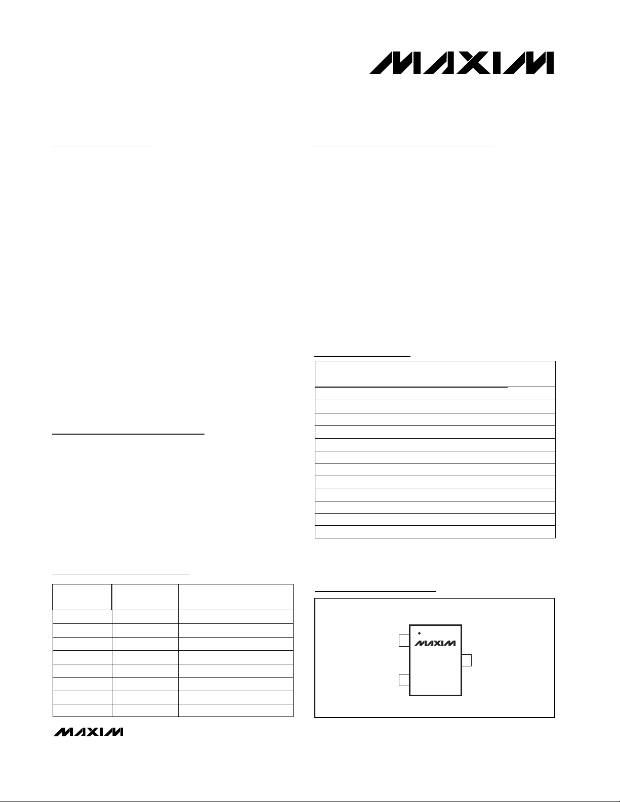
TOP VIEW
OUT
1
IN
2
MAX6061–
MAX6068
SOT23-3
3 GND

MAX6061–MAX6068
Precision, Micropower, Low-Dropout,
High-Output-Current, SOT23 Voltage References
2 _______________________________________________________________________________________
ABSOLUTE MAXIMUM RATINGS
ELECTRICAL CHARACTERISTICS—MAX6061, V
OUT
= 1.25V
(VIN= +5V, I
OUT
= 0, TA= T
MIN
to T
MAX
, unless otherwise noted. Typical values are at TA= +25°C.) (Note 1)
Stresses beyond those listed under “Absolute Maximum Ratings” may cause permanent damage to the device. These are stress ratings only, and functional
operation of the device at these or any other conditions beyond those indicated in the operational sections of the specifications is not implied. Exposure to
absolute maximum rating conditions for extended periods may affect device reliability.
(Voltages Referenced to GND)
IN .........................................................................-0.3V to +13.5V
OUT .............................................................-0.3V to (V
IN
+ 0.3V)
Output Short-Circuit Duration to GND or IN (VIN< 6V)...Continuous
Output Short-Circuit Duration to GND or IN (VIN≥ 6V)................60s
Continuous Power Dissipation (T
A
= +70°C)
3-Pin SOT23 (derate 4.0mW/°C above +70°C)............320mW
Operating Temperature Range ...........................-40°C to +85°C
Storage Temperature Range .............................-65°C to +150°C
Lead Temperature (soldering, 10s) .................................+300°C
Output Voltage V
Output Voltage Temperature
Coefficient (Note 2)
Line Regulation
Load Regulation
OUT Short-Circuit Current I
Long-Term Stability
Output Voltage Hysteresis (Note 3)
DYNAMIC CHARACTERISTICS
Noise Voltage e
Ripple Rejection
Turn-On Settling Time t
INPUT CHARACTERISTICS
Supply Voltage Range V
Quiescent Supply Current I
Change in Supply Current
PARAMETER SYMBOL CONDITIONS MIN TYP MAX UNITS
OUT
TCV
∆V
∆V
∆V
∆I
∆V
time
∆V
cycle
OUT
∆V
∆V
∆I
∆V
TA = +25°C
MAX6061A 6 20
OUT
MAX6061B 6 30
/
OUT
2.5V ≤ VIN ≥ 12.6V 10 90 µV/V
IN
Sourcing: 0 ≤ I
/
OUT
OUT Sinking: -2mA ≤ I
Short to GND 25
SC
Short to IN 25
/
OUT
1000hr at +25°C62
/
OUT
f = 0.1Hz to 10Hz 13 µVp-p
f = 10Hz to 10kHz 15 µV
/
OUT
V
= 5V ± 100mV, f = 120Hz 86 dB
IN
IN
R
IN
IN
/
IN
IN
To V
Guaranteed by line regulation test
2.5V ≤ VIN ≤ 12.6V 3.4 8.0 µA/V
= 0.1% of final value, C
OUT
MAX6061A (0.32%) 1.244 1.248 1.252
MAX6061B (0.48%) 1.242 1.248 1.254
≤ 5mA 0.5 0.9
OUT
≤ 0 1.3 3.0
OUT
130 ppm
= 50pF 50 µs
OUT
2.5
90 125 µA
V
ppm/°C
mV/mA
mA
ppm/
1000hr
RMS
12.6 V
MAX6061–MAX6068
Precision, Micropower, Low-Dropout,
High-Output-Current, SOT23 Voltage References
_______________________________________________________________________________________ 3
ELECTRICAL CHARACTERISTICS—MAX6068, V
OUT
= 1.80V
(VIN= +5V, TA= T
MIN
to T
MAX
, unless otherwise noted. Typical values are at TA= +25°C.) (Note 1)
Output Voltage V
Output Voltage Temperature
Coefficient (Note 2)
Line Regulation
Load Regulation
OUT Short-Circuit Current I
Long-Term Stability
Output Voltage Hysteresis (Note 3)
DYNAMIC CHARACTERISTICS
Noise Voltage e
Ripple Rejection
Turn-On Settling Time t
INPUT CHARACTERISTICS
Supply Voltage Range V
Quiescent Supply Current I
Change in Supply Current
PARAMETER SYMBOL CONDITIONS MIN TYP MAX UNITS
OUT
TCV
∆V
∆V
∆V
∆I
OUT Sinking: -2mA ≤ I
SC
∆V
time
∆V
cycle
OUT
∆V
∆V
∆I
∆V
TA = +25°C
MAX6068A 6 20
OUT
MAX6068B 6 30
/
OUT
2.5V ≤ VIN ≥ 12.6V 33 200 µV/V
IN
Sourcing: 0 ≤ I
/
OUT
Short to GND 25
Short to IN 25
/
OUT
1000hr at +25°C62
/
OUT
f = 0.1Hz to 10Hz 22 µVp-p
f = 10Hz to 10kHz 25 µV
/
OUT
V
= 5V ±100mV, f = 120Hz 86 dB
IN
IN
R
IN
IN
/
IN
IN
To V
Guaranteed by line regulation test 2.5 12.6 V
2.5V ≤ VIN ≤ 12.6V 3.3 8.0 µA/V
= 0.1% of final value, C
OUT
≤ 5mA 0.5 0.9
OUT
≤ 0 1.5 4
OUT
MAX6068A (0.17%) 1.797 1.800 1.803
MAX6068B (0.39%) 1.793 1.800 1.807
130 ppm
= 50pF 115 µs
OUT
90 125 µA
V
ppm/°C
mV/mA
mA
ppm/
1000hr
RMS
MAX6061–MAX6068
Precision, Micropower, Low-Dropout,
High-Output-Current, SOT23 Voltage References
4 _______________________________________________________________________________________
ELECTRICAL CHARACTERISTICS—MAX6062, V
OUT
= 2.048V
(VIN= +5V, I
OUT
= 0, TA= T
MIN
to T
MAX
, unless otherwise noted. Typical values are at TA= +25°C.) (Note 1)
MAX6062B (0.39%)
MAX6062A (0.24%)
Output Voltage V
OUT
2.043 2.048 2.053
PARAMETER SYMBOL MIN TYP MAX UNITS
OUT Short-Circuit Current I
SC
25
mA
1.5 4
Load Regulation
∆V
OUT
/
∆I
OUT
0.5 0.9
mV/mA
Line Regulation
∆V
OUT
/
∆V
IN
33 200
µV/V
25
Long-Term Stability
∆V
OUT
/
time
62
ppm/
1000hr
Output Voltage Hysteresis
(Note 3)
∆V
OUT
/
cycle
130
ppm
Output Voltage Temperature
Coefficient (Note 2)
2.040 2.048 2.056
TCV
OUT
620
ppm/°C
630
Noise Voltage e
OUT
22
µVp-p
25
µV
RMS
Ripple Rejection
∆V
OUT
/
∆V
IN
86
dB
Turn-On Settling Time t
R
115
µs
Supply Voltage Range V
IN
2.5 12.6
V
Quiescent Supply Current I
IN
90 125
µA
Change in Supply Current IIN/V
IN
3.3 8.0
µA/V
CONDITIONS
f = 0.1Hz to 10Hz
Short to GND
f = 10Hz to 10kHz
Sinking: -2mA ≤ I
OUT
≤ 0
Sourcing: 0 ≤ I
OUT
≤ 5mA
2.5V ≤ VIN≤ 12.6V
Short to IN
1000hr at +25°C
VIN= 5V ±100mV, f = 120Hz
To V
OUT
= 0.1% of final value, C
OUT
= 50pF
Guaranteed by line-regulation test
TA= +25°C
MAX6062A
2.5V ≤ VIN≤ 12.6V
MAX6062B
V
DYNAMIC CHARACTERISTICS
INPUT CHARACTERISTICS
MAX6061–MAX6068
Precision, Micropower, Low-Dropout,
High-Output-Current, SOT23 Voltage References
_______________________________________________________________________________________ 5
ELECTRICAL CHARACTERISTICS—MAX6066, V
OUT
= 2.500V
(VIN= +5V, I
OUT
= 0, TA= T
MIN
to T
MAX
, unless otherwise noted. Typical values are at TA= +25°C.) (Note 1)
MAX6066B (0.4%)
MAX6066A (0.2%)
TA= +25°C V
2.495 2.500 2.505
V
OUT
Output Voltage
MAX6066B
(V
OUT
+ 0.2V) ≤ VIN≤ 12.6V
MAX6066A
Guaranteed by line-regulation test
To V
OUT
= 0.1% of final value, C
OUT
= 50pF
VIN= 5V ±100mV, f = 120Hz
1000hr at +25°C
Short to IN
(V
OUT
+ 0.2V) ≤ VIN≤ 12.6V
Sourcing: 0 ≤ I
OUT
≤ 5mA
Sinking: -2mA ≤ I
OUT
≤ 0
f = 10Hz to 10kHz
Short to GND
f = 0.1Hz to 10Hz
CONDITIONS
µA/V
3.3 8.0
IIN/V
IN
Change in Supply Current
µA
90 125
I
IN
Quiescent Supply Current
V
V
OUT
+ 0.2 12.6
V
IN
Supply Voltage Range
µs
115
t
R
Turn-On Settling Time
dB
86
∆V
OUT
/
∆V
IN
Ripple Rejection
µV
RMS
30
µVp-p
27
e
OUT
Noise Voltage
630
ppm/°C
620
TCV
OUT
2.490 2.500 2.510
Output Voltage Temperature
Coefficient (Note 2)
ppm
130
∆V
OUT
/
cycle
Output Voltage Hysteresis
(Note 3)
ppm/
1000hr
62
∆V
OUT
/
time
Long-Term Stability
25
µV/V
60 300
∆V
OUT
/
∆V
IN
Line Regulation
mV/mA
0.5 0.9
∆V
OUT
/
∆I
OUT
Load Regulation
1.6 5
mA
25
I
SC
OUT Short-Circuit Current
UNITSMIN TYP MAXSYMBOLPARAMETER
I
OUT
= 1mA mV
50 200
V
IN
-
V
OUT
Dropout Voltage (Note 4)
DYNAMIC CHARACTERISTICS
INPUT CHARACTERISTICS

MAX6061–MAX6068
Precision, Micropower, Low-Dropout,
High-Output-Current, SOT23 Voltage References
6 _______________________________________________________________________________________
Output Voltage
ELECTRICAL CHARACTERISTICS—MAX6063, V
OUT
= 3.0V
(VIN= +5V, I
OUT
= 0, TA= T
MIN
to T
MAX
, unless otherwise noted. Typical values are at TA= +25°C.) (Note 1)
UNITSMIN TYP MAXCONDITIONSSYMBOLPARAMETER
Output Voltage V
OUT
TA= +25°C
MAX6063A (0.2%)
MAX6063B (0.4%)
2.994 3.000 3.006
2.988 3.000 3.012
V
ppm/°C
620
630
MAX6063A
MAX6063B
TCV
OUT
Output Voltage Temperature
Coefficient (Note 2)
Line Regulation
∆V
OUT
/
∆V
IN
(V
OUT
+ 0.2V) ≤ VIN≤ 12.6V
90 400
µV/V
mV/mA
0.5 0.9
2.0 6.0
Sourcing: 0 ≤ I
OUT
≤ 5mA
Sinking: -2mA ≤ I
OUT
≤ 0
∆V
OUT
/
∆I
OUT
Load Regulation
Dropout Voltage (Note 4)
V
IN
-
V
OUT
I
OUT
= 1mA
50 200
mV
mA
25
25
Short to GND
Short to IN
I
SC
OUT Short-Circuit Current
Long-Term Stability
∆V
OUT
/
time
1000hr at +25°C
62
ppm/
1000hr
ppm
130
∆V
OUT
/
cycle
Output Voltage Hysteresis
(Note 3)
µVp-p
35
f = 0.1Hz to 10Hz
e
OUT
Noise Voltage
f = 10Hz to 10kHz
40
µV
RMS
dB
76
VIN= 5V ±100mV, f = 120Hz
∆V
OUT
/
∆V
IN
Ripple Rejection
Turn-On Settling Time t
R
To V
OUT
= 0.1% of final value, C
OUT
= 50pF
115
µs
V
V
OUT
+ 0.2 12.6
Guaranteed by line-regulation testV
IN
Supply Voltage Range
Quiescent Supply Current I
IN
90 125
µA
µA/V
3.4 8.0
(V
OUT
+ 0.2V) ≤ VIN≤ 12.6VIIN/V
IN
Change in Supply Current
INPUT CHARACTERISTICS
DYNAMIC CHARACTERISTICS

MAX6061–MAX6068
Precision, Micropower, Low-Dropout,
High-Output-Current, SOT23 Voltage References
_______________________________________________________________________________________ 7
ELECTRICAL CHARACTERISTICS—MAX6064, V
OUT
= 4.096V
(VIN= +5V, I
OUT
= 0, TA= T
MIN
to T
MAX
, unless otherwise noted. Typical values are at TA= +25°C.) (Note 1)
UNITSMIN TYP MAXCONDITIONSSYMBOLPARAMETER
Output Voltage V
OUT
TA= +25°C
MAX6064A (0.2%)
4.088 4.096 4.104
4.080 4.096 4.112
V
ppm/°C
620
630
MAX6064A
MAX6064B
TCV
OUT
Output Voltage Temperature
Coefficient (Note 2)
Line Regulation
∆V
OUT
/
∆V
IN
(V
OUT
+ 0.2V) ≤ VIN≤ 12.6V
130 430
µV/V
mV/mA
0.5 0.9
2.2 8
Sourcing: 0 ≤ I
OUT
≤ 5mA
Sinking: -2mA ≤ I
OUT
≤ 0
∆V
OUT
/
∆I
OUT
Load Regulation
Dropout Voltage (Note 4)
V
IN
-
V
OUT
I
OUT
= 1mA
50 200
mV
mA
25
25
Short to GND
Short to IN
I
SC
OUT Short-Circuit Current
Long-Term Stability
∆V
OUT
/
time
1000hr at +25°C
62
ppm/
1000hr
ppm
130
∆V
OUT
/
cycle
Output Voltage Hysteresis
(Note 3)
µVp-p
50
f = 0.1Hz to 10Hz
e
OUT
Noise Voltage
f = 10Hz to 10kHz
50
µV
RMS
dB
72
VIN= 5V ±100mV, f = 120Hz
∆V
OUT
/
∆V
IN
Ripple Rejection
Turn-On Settling Time t
R
To V
OUT
= 0.1% of final value, C
OUT
= 50pF
190
µs
V
V
OUT
+ 0.2 12.6
Guaranteed by line-regulation testV
IN
Supply Voltage Range
Quiescent Supply Current I
IN
90 125
µA
µA/V
3.2 8.0
(V
OUT
+ 0.2V) ≤ VIN≤ 12.6VIIN/V
IN
Change in Supply Current
MAX6064B (0.4%)
INPUT CHARACTERISTICS
DYNAMIC CHARACTERISTICS

MAX6061–MAX6068
Precision, Micropower, Low-Dropout,
High-Output-Current, SOT23 Voltage References
8 _______________________________________________________________________________________
ELECTRICAL CHARACTERISTICS—MAX6067, V
OUT
= 4.500V
(VIN= +5V, I
OUT
= 0, TA= T
MIN
to T
MAX
, unless otherwise noted. Typical values are at TA= +25°C.) (Note 1)
Dropout Voltage (Note 4)
V
IN
-
V
OUT
50 200
mVI
OUT
= 1mA
PARAMETER SYMBOL MIN TYP MAX UNITS
OUT Short-Circuit Current I
SC
25
mA
2.4 8
Load Regulation
∆V
OUT
/
∆I
OUT
0.5 0.9
mV/mA
Line Regulation
∆V
OUT
/
∆V
IN
170 550
µV/V
25
Long-Term Stability
∆V
OUT
/
time
62
ppm/
1000hr
Output Voltage Hysteresis
(Note 3)
∆V
OUT
/
cycle
130
ppm
Output Voltage Temperature
Coefficient (Note 2)
4.482 4.500 4.518
TCV
OUT
620
ppm/°C
630
Noise Voltage e
OUT
55
µVp-p
55
µV
RMS
Ripple Rejection
∆V
OUT
/
∆V
IN
70
dB
Turn-On Settling Time t
R
230
µs
Supply Voltage Range V
IN
V
OUT
+ 0.2 12.6
V
Quiescent Supply Current I
IN
90 125
µA
Change in Supply Current IIN/V
IN
3.2 8.0
µA/V
CONDITIONS
f = 0.1Hz to 10Hz
Short to GND
f = 10Hz to 10kHz
Sinking: -2mA ≤ I
OUT
≤ 0
Sourcing: 0 ≤ I
OUT
≤ 5mA
(V
OUT
+ 0.2V) ≤ VIN≤ 12.6V
Short to IN
1000hr at +25°C
VIN= 5V ±100mV, f = 120Hz
To V
OUT
= 0.1% of final value, C
OUT
= 50pF
Guaranteed by line-regulation test
MAX6067A
(V
OUT
+ 0.2V) ≤ VIN≤ 12.6V
MAX6067B
MAX6067B (0.4%)
Output Voltage V
OUT
4.491 4.500 4.509
V
TA= +25°C
MAX6067A (0.2%)
DYNAMIC CHARACTERISTICS
INPUT CHARACTERISTICS

MAX6061–MAX6068
Precision, Micropower, Low-Dropout,
High-Output-Current, SOT23 Voltage References
_______________________________________________________________________________________ 9
ELECTRICAL CHARACTERISTICS—MAX6065, V
OUT
= 5.000V
(VIN= +5.2V, I
OUT
= 0, TA= T
MIN
to T
MAX
, unless otherwise noted. Typical values are at TA= +25°C.) (Note 1)
Note 1: All devices are 100% production tested at T
A
= +25°C and are guaranteed by design for TA= T
MIN
to T
MAX
, as specified.
Note 2: Temperature Coefficient is measured by the “box” method, i.e., the maximum ∆V
OUT
is divided by the maximum ∆T.
Note 3: Temperature Hysteresis is defined as the change in +25°C output voltage before and after cycling the device from T
MIN
to T
MAX
.
Note 4: Dropout voltage is the minimum input voltage at which V
OUT
changes ≤ 0.2% from V
OUT
at VIN= 5.0V (VIN= 5.5V for MAX6065).
V
OUT
4.990 5.000 5.010
VTA= +25°C
MAX6065A (0.2%)
MAX6065B (0.4%)
PARAMETER SYMBOL MIN TYP MAX UNITS
OUT Short-Circuit Current I
SC
25
mA
2.4 8.0
Load Regulation
∆V
OUT
/
∆I
OUT
0.5 0.9
mV/mA
Line Regulation
∆V
OUT
/
∆V
IN
180 550
µV/V
25
Long-Term Stability
∆V
OUT
/
time
62
ppm/
1000hr
Output Voltage Hysteresis
(Note 3)
∆V
OUT
/
cycle
130
ppm
Output Voltage Temperature
Coefficient (Note 2)
4.980 5.000 5.020
TCV
OUT
620
ppm/°C
630
Noise Voltage e
OUT
60
µVp-p
60
µV
RMS
Ripple Rejection
∆V
OUT
/
∆V
IN
65
dB
Turn-On Settling Time t
R
300
µs
Supply Voltage Range V
IN
V
OUT
+ 0.2 12.6
V
Quiescent Supply Current I
IN
90 125
µA
Change in Supply Current IIN/V
IN
3.2 8.0
µA/V
Dropout Voltage (Note 4)
V
IN
-
V
OUT
CONDITIONS
f = 0.1Hz to 10Hz
Short to GND
f = 10Hz to 10kHz
Sinking: -2mA ≤ I
OUT
≤ 0
Sourcing: 0 ≤ I
OUT
≤ 5mA
(V
OUT
+ 0.2V) ≤ VIN≤ 12.6V
Short to IN
1000hr at +25°C
VIN= 5V ±100mV, f = 120Hz
To V
OUT
= 0.1% of final value, C
OUT
= 50pF
Guaranteed by line-regulation test
MAX6065A
(V
OUT
+ 0.2V) ≤ VIN≤ 12.6V
50 200
MAX6065B
mVI
OUT
= 1mA
Output Voltage
DYNAMIC CHARACTERISTICS
INPUT CHARACTERISTICS

MAX6061–MAX6068
Precision, Micropower, Low-Dropout,
High-Output-Current, SOT23 Voltage References
10 ______________________________________________________________________________________
Typical Operating Characteristics
(VIN= +5V for MAX6061–MAX6068, VIN= +5.5V for MAX6065, I
OUT
= 0, TA= +25°C, unless otherwise noted.) (Note 5)
2.046
2.047
2.049
2.048
2.050
2.051
-40 10-15 35 60 85
MAX6062
OUTPUT VOLTAGE TEMPERATURE DRIFT
MAX6061/68 toc01
TEMPERATURE (°C)
OUTPUT VOLTAGE (V)
THREE TYPICAL PARTS
4.998
4.999
5.001
5.000
5.002
5.003
-40 10-15 35 60 85
MAX6065
OUTPUT VOLTAGE TEMPERATURE DRIFT
MAX6061/68 toc02
TEMPERATURE (°C)
OUTPUT VOLTAGE (V)
THREE
TYPICAL PARTS
-300
-200
-100
0
100
200
300
2 4 6 8 10 12
MAX6061
LINE REGULATION
MAX6061/68 toc03
INPUT VOLTAGE (V)
OUTPUT VOLTAGE CHANGE (
µ
V)
TA = +85°C
TA = +25°C
TA = -40°C
-1200
-600
-800
-1000
-400
-200
0
200
5971113
MAX6065
LINE REGULATION
MAX6061/68 toc04
INPUT VOLTAGE (V)
OUTPUT VOLTAGE CHANGE (µV)
TA = +85°C
TA = +25°C
TA = -40°C
-3
1
0
-1
-2
2
3
4
5
-4 -2 0 2 4
MAX6061/68 toc05
LOAD CURRENT (mA)
OUTPUT VOLTAGE CHANGE (mV)
TA = +25°C
TA = -40°C
MAX6061
LOAD REGULATION
TA = +85°C
-6
2
0
-2
-4
4
8
6
10
12
-6 -2-4 0 2 4 6
MAX6061/68 toc06
LOAD CURRENT (mA)
OUTPUT VOLTAGE CHANGE (mV)
MAX6065
LOAD REGULATION
TA = +25°C
TA = +85°C
TA = -40°C
0
0.10
0.05
0.20
0.15
0.25
0.30
021345
MAX6066
DROPOUT VOLTAGE
vs. LOAD CURRENT
MAX6061/68 toc07
LOAD CURRENT (mA)
DROPOUT VOLTAGE (V)
TA = +85°C
TA = +25°C
TA = -40°C
0
0.05
0.15
0.10
0.20
0.25
021345
TA = +85°C
TA = +25°C
TA = -40°C
MAX6061/68 toc08
LOAD CURRENT (mA)
DROPOUT VOLTAGE (V)
MAX6065
DROPOUT VOLTAGE
vs. LOAD CURRENT
POWER-SUPPLY REJECTION RATIO
MAX6061
vs. FREQUENCY
0
-10
-20
-30
-40
-50
PSRR (dB)
-60
-70
-80
-90
0.001 1 10 1000.01 0.1 1000
FREQUENCY (kHz)
MAX6061/68 toc09

MAX6061–MAX6068
Precision, Micropower, Low-Dropout,
High-Output-Current, SOT23 Voltage References
______________________________________________________________________________________ 11
Typical Operating Characteristics (continued)
(VIN= +5V for MAX6061–MAX6068, VIN= +5.5V for MAX6065, I
OUT
= 0, TA= +25°C, unless otherwise noted.) (Note 5)
V
OUT
10µV/div
1s/div
MAX6065
NOISE
MAX6061/68 toc18
POWER-SUPPLY REJECTION RATIO
0
-10
-20
-30
-40
PSRR (dB)
-50
-60
-70
-80
0.001 10 1000
120
110
100
90
SUPPLY CURRENT (µA)
80
70
-40 10-15 35 60 85
180
160
140
120
100
80
60
OUTPUT IMPEDANCE (Ω)
40
20
0
0.001 10 1000
MAX6065
vs. FREQUENCY
0.1
FREQUENCY (kHz)
MAX6061
SUPPLY CURRENT
vs. TEMPERATURE
VIN = 12.5V
VIN = 7.5V
VIN = 2.5V
VIN = 5.5V
TEMPERATURE (°C)
MAX6065
OUTPUT IMPEDANCE
vs. FREQUENCY
0.1
FREQUENCY (kHz)
MAX6061/68 toc10
MAX6061/68 toc13
MAX6061/68 toc16
110
100
A)
µ
90
SUPPLY CURRENT (
80
70
24681012
115
A)
µ
105
95
SUPPLY CURRENT (
85
-40 10-15 35 60 85
0.1Hz TO 10Hz OUTPUT NOISE
V
OUT
10µV/div
MAX6061
SUPPLY CURRENT
vs. INPUT VOLTAGE
115
110
MAX6061/68 toc11
A)
105
µ
100
95
SUPPLY CURRENT (
90
85
80
5791113
INPUT VOLTAGE (V)
MAX6065
SUPPLY CURRENT
vs. TEMPERATURE
220
200
180
)
MAX6061/68 toc14
Ω
VIN = 12.5V
VIN = 7.5V
VIN = 5.5V
TEMPERATURE (°C)
160
140
120
100
80
OUTPUT IMPEDANCE (
60
40
20
0
0.001 10 1000
MAX6061
MAX6061/68 toc17
1s/div
MAX6065
SUPPLY CURRENT
vs. INPUT VOLTAGE
MAX6061/68 toc12
INPUT VOLTAGE (V)
MAX6061
OUTPUT IMPEDANCE
vs. FREQUENCY
MAX6061/68 toc15
0.1
FREQUENCY (kHz)

MAX6061–MAX6068
Precision, Micropower, Low-Dropout,
High-Output-Current, SOT23 Voltage References
12 ______________________________________________________________________________________
Typical Operating Characteristics (continued)
(VIN= +5V for MAX6061–MAX6068, VIN= +5.5V for MAX6065, I
OUT
= 0, TA= +25°C, unless otherwise noted.) (Note 5)
I
OUT
500µA/div
V
OUT
AC-COUPLED
20mV/div
400µs/div
MAX6065
LOAD TRANSIENT
(I
OUT
= ±250µA, CL = 1µF, V
IN
= 5.5V)
+250µA
-250µA
MAX6061/68 toc24
V
OUT
500mV/div
V
IN
5V/div
MAX6061
TURN-ON TRANSIENT
(C
L
= 50pF)
MAX6061/68 toc19
V
OUT
2V/div
V
IN
5V/div
40µs/div
MAX6065
TURN-ON TRANSIENT
(C
L
= 50pF)
MAX6061/68 toc20
I
OUT
500µA/div
V
OUT
AC-COUPLED
100mV/div
400µs/div
MAX6061
LOAD TRANSIENT
(I
OUT
= ±250µA, V
IN
= 5.0, CL = 0)
I
OUT
+250µA
I
OUT
-250µA
MAX6061/68 toc21
I
OUT
500µA/div
V
OUT
AC-COUPLED
50mV/div
400µs/div
MAX6065
LOAD TRANSIENT
(I
OUT
= ±250µA, CL = 0, V
IN
= 5.5V)
+250µA
-250µA
MAX6061/68 toc22
I
OUT
500µA/div
V
OUT
AC-COUPLED
10mV/div
400µs/div
MAX6061
LOAD TRANSIENT
(I
OUT
= ±250µA, V
IN
= 5.0V, CL = 1µF)
+250µA
-250µA
MAX6061/68 toc23

MAX6061–MAX6068
Precision, Micropower, Low-Dropout,
High-Output-Current, SOT23 Voltage References
______________________________________________________________________________________ 13
Typical Operating Characteristics (continued)
(VIN= +5V for MAX6061–MAX6068, VIN= +5.5V for MAX6065, I
OUT
= 0, TA= +25°C, unless otherwise noted.) (Note 5)
I
OUT
5mA/div
V
OUT
AC-COUPLED
100mV/div
400µs/div
MAX6061
LOAD TRANSIENT
(V
IN
= 5.0V, CL = 0, I
OUT
= ±2mA)
+2mA
-2mA
MAX6061/68 toc25
I
OUT
5mA/div
V
OUT
AC-COUPLED
50mV/div
400µs/div
MAX6065
LOAD TRANSIENT
(C
L
= 0, I
OUT
= ±2mA, V
IN
= 5.5V)
+2mA
-2mA
MAX6061/68 toc26
I
OUT
5mA/div
V
OUT
AC-COUPLED
50mV/div
400µs/div
MAX6061
LOAD TRANSIENT
(V
IN
= 5.0V, CL = 1µF, I
OUT
= ±2mA)
+2mA
-2mA
MAX6061/68 toc27
I
OUT
5mA/div
V
OUT
AC-COUPLED
20mV/div
400µs/div
MAX6065
LOAD TRANSIENT
(C
L
= 1µF, I
OUT
= ±2mA, V
IN
= 5.5V)
+2mA
-2mA
MAX6061/68 toc28
I
OUT
5mA/div
V
OUT
AC-COUPLED
200mV/div
400µs/div
MAX6061
LOAD TRANSIENT
(V
IN
= 5.0V, CL = 0, I
OUT
= ±4mA)
+4mA
-4mA
MAX6061/68 toc29
I
OUT
5mA/div
V
OUT
AC-COUPLED
100mV/div
400µs/div
MAX6065
LOAD TRANSIENT
(I
OUT
= ±5mA, CL = 0, V
IN
= 5.5V)
+5mA
-5mA
MAX6061/68 toc30

MAX6061–MAX6068
Precision, Micropower, Low-Dropout,
High-Output-Current, SOT23 Voltage References
14 ______________________________________________________________________________________
Typical Operating Characteristics (continued)
(VIN= +5V for MAX6061–MAX6068, VIN= +5.5V for MAX6065, I
OUT
= 0, TA= +25°C, unless otherwise noted.) (Note 5)
I
OUT
5mA/div
V
OUT
AC-COUPLED
50mV/div
400µs/div
MAX6061
LOAD TRANSIENT
(V
IN
= 5.0V, CL = 1µF, I
OUT
= ±4mA)
+4mA
-4mA
MAX6061/68 toc31
Note 5: Many of the MAX6061 family Typical Operating Characteristics are extremely similar. The extremes of these characteristics
are found in the MAX6061 (1.25V output) and the MAX6065 (5.0V output). The Typical Operating Characteristics of the
remainder of the MAX6061 family, typically lie between these two extremes and can be estimated based on their output
voltages.
MAX6065
LOAD TRANSIENT
= ±5mA, CL = 1µF, V
(I
OUT
I
OUT
5mA/div
V
OUT
AC-COUPLED
50mV/div
400µs/div
= 5.5V)
IN
MAX6061/68 toc32
+5mA
-5mA
V
IN
500mV/div
V
OUT
AC-COUPLED
20mV/div
MAX6061
LINE TRANSIENT
= 0)
(C
L
40µs/div
MAX6061/68 toc33
+0.25
-0.25
V
500mV/div
V
OUT
AC-COUPLED
20mV/div
IN
MAX6065
LINE TRANSIENT
= 0)
(C
L
40µs/div
MAX6061/68 toc34
+0.25
-0.25

MAX6061–MAX6068
Precision, Micropower, Low-Dropout,
High-Output-Current, SOT23 Voltage References
______________________________________________________________________________________ 15
Applications Information
Input Bypassing
For the best line-transient performance, decouple the
input with a 0.1µF ceramic capacitor as shown in the
Typical Operating Circuit. Locate the capacitor as close
to IN as possible. Where transient performance is less
important, no capacitor is necessary.
Output/Load Capacitance
Devices in the MAX6061 family do not require an output
capacitance for frequency stability. In applications
where the load or the supply can experience step
changes, an output capacitor of at least 0.1µF will
reduce the amount of overshoot (undershoot) and
improve the circuit’s transient response. Many applications do not require an external capacitor, and the
MAX6061 family can offer a significant advantage in
these applications when board space is critical.
Supply Current
The quiescent supply current of the series-mode
MAX6061 family is typically 90µA and is virtually independent of the supply voltage, with only an 8µA/V (max)
variation with supply voltage. Unlike series references,
shunt-mode references operate with a series resistor
connected to the power supply. The quiescent current
of a shunt-mode reference is thus a function of the input
voltage. Additionally, shunt-mode references have to
be biased at the maximum expected load current, even
if the load current is not present at the time. In the
MAX6061 family, the load current is drawn from the
input voltage only when required, so supply current is
not wasted and efficiency is maximized at all input voltages. This improved efficiency reduces power dissipation and extends battery life. When the supply voltage
is below the minimum specified input voltage (as during
turn-on), the devices can draw up to 400µA beyond the
nominal supply current. The input voltage source must
be capable of providing this current to ensure reliable
turn-on.
Output Voltage Hysteresis
Output voltage hysteresis is the change of output voltage
at TA= +25°C before and after the device is cycled
over its entire operating temperature range. Hysteresis
is caused by differential package stress appearing
across the bandgap core transistors. The typical temperature hysteresis value is 130ppm.
Turn-On Time
These devices typically turn on and settle to within 0.1%
of their final value in 50µs to 300µs, depending on the
device. The turn-on time can increase up to 1.5ms with
the device operating at the minimum dropout voltage and
the maximum load.
Chip Information
TRANSISTOR COUNT: 117
PROCESS: BiCMOS
Pin Description
PIN NAME FUNCTION
1 IN Input Voltage
2 OUT Reference Output
3 GND Ground
Typical Operating Circuit
Ordering Information (continued)
PART TEMP. RANGE
PINPACKAGE
TOP
MARK
MAX6067AEUR-T
-40°C to +85°C 3 SOT23-3 FZFS
MAX6067BEUR-T -40°C to +85°C 3 SOT23-3 FZFT
MAX6068AEUR-T
-40°C to +85°C 3 SOT23-3 FZIB
MAX6068BEUR-T -40°C to +85°C 3 SOT23-3 FZIC
+SUPPLY INPUT (SEE
*
*CAPACITORS ARE OPTIONAL.
SELECTOR GUIDE
IN
MAX6061MAX6068
GND
)
OUT REFERENCE
OUT
1µF *

MAX6061–MAX6068
Precision, Micropower, Low-Dropout,
High-Output-Current, SOT23 Voltage References
Package Information
Maxim cannot assume responsibility for use of any circuitry other than circuitry entirely embodied in a Maxim product. No circuit patent licenses are
implied. Maxim reserves the right to change the circuitry and specifications without notice at any time.
16 ____________________Maxim Integrated Products, 120 San Gabriel Drive, Sunnyvale, CA 94086 408-737-7600
© 2001 Maxim Integrated Products Printed USA is a registered trademark of Maxim Integrated Products.
SOTPO3L.EPS
 Loading...