

Page 1
General Description
The MAX6043 precision voltage reference provides
accurate preset +2.5V, +3.3V, +4.096V, +5.0V, and
+10V reference voltages from up to +40V input voltages. The MAX6043 features a proprietary temperature
coefficient curvature-correction circuit and lasertrimmed thin-film resistors that result in a very low temperature coefficient of 15ppm/°C (max) and excellent
initial accuracy of 0.05% (max). Low temperature drift
and low noise make the MAX6043 ideal for use with
high-resolution A/D or D/A converters.
The MAX6043 draws 320µA of supply current and
sources 10mA or sinks 0.6mA of load current. The
MAX6043 uses bandgap technology for low-noise performance and excellent accuracy. The MAX6043 does
not require an output bypass capacitor for stability, and
is stable with capacitive loads up to 100µF. Eliminating
the output bypass capacitor saves valuable board area
in space-critical applications. The supply-independent,
low supply current makes the MAX6043 ideal for battery-operated, high-performance systems.
The MAX6043 is available in a 6-pin SOT23 package
and operates over the automotive (-40°C to +125°C)
temperature range.
Applications
Analog-to-Digital Converters
Digital-to-Analog Converters
Digital Voltmeters
Voltage Regulators
Threshold Detectors
Features
♦ +2.5V, +3.3V, +4.096V, +5.0V, or +10V Output
Voltages
♦ Excellent Temperature Stability: 15ppm/°C (max)
♦ Tight Initial Accuracy: 0.05% (max)
♦ Tiny SOT23 Package
♦ Wide +4.5V to +40V Supply Voltage Range
♦ Low Noise: 4µV
P-P
(typ at 2.5V Output)
♦ Short-Circuit Protected
♦ Wide Operating Temperature Range
-40°C to +125°C
♦ Stable with Capacitive Loads from 0 to 100µF
♦ No External Capacitors Required for Stability
MAX6043
Precision High-Voltage Reference in SOT23
________________________________________________________________ Maxim Integrated Products 1
19-3036; Rev 1; 5/04
For pricing, delivery, and ordering information, please contact Maxim/Dallas Direct! at
1-888-629-4642, or visit Maxim’s website at www.maxim-ic.com.
Ordering Information
Ordering Information continued at end of data sheet.
Typical Operating Circuit appears at end of data sheet.
Selector Guide
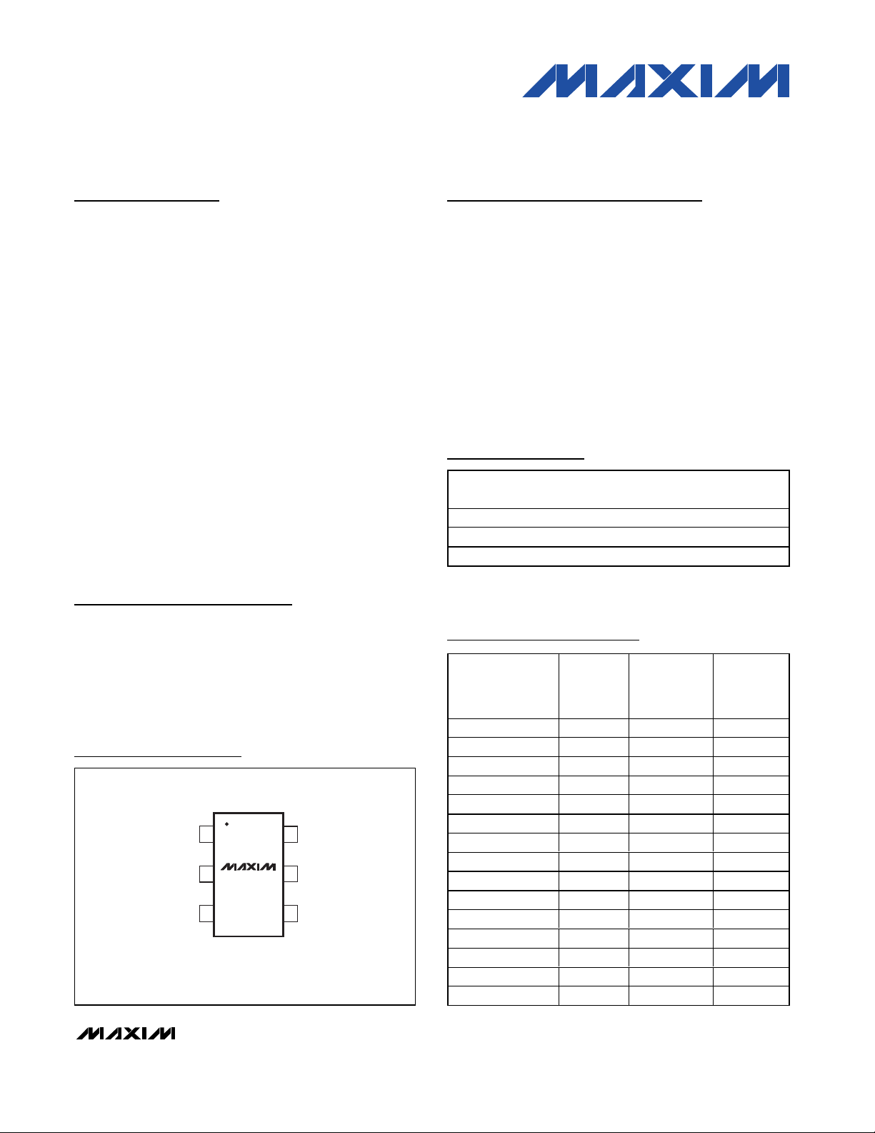
Pin Configuration
TOP VIEW
16OUTS
I.C.*
GND
2
MAX6043
34
SOT23-6
*INTERNALLY CONNECTED. DO NOT CONNECT.
5 OUTF
INI.C.*
PART TEMP RANGE
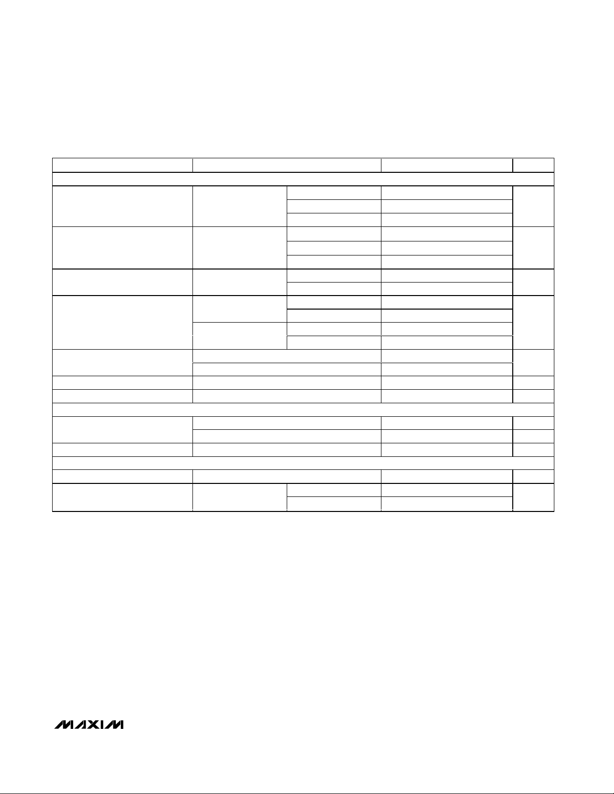
MAX6043AAUT25-T -40°C to +125°C 6 SOT23-6 ABRZ
MAX6043BAUT25-T -40°C to +125°C 6 SOT23-6 ABDQ
MAX6043CAUT25-T -40°C to +125°C 6 SOT23-6 ABDR
PART
MAX6043AAUT25 2.5 15 0.06
MAX6043BAUT25 2.5 20 0.1
MAX6043CAUT25 2.5 65 0.5
MAX6043AAUT33 3.3 15 0.06
MAX6043BAUT33 3.3 20 0.1
MAX6043CAUT33 3.3 65 0.5
MAX6043AAUT41 4.096 15 0.06
MAX6043BAUT41 4.096 20 0.1
MAX6043CAUT41 4.096 65 0.5
MAX6043AAUT50 5.0 15 0.06
MAX6043BAUT50 5.0 20 0.1
MAX6043CAUT50 5.0 65 0.5
MAX6043AAUT10 10.0 15 0.05
MAX6043BAUT10 10.0 20 0.1
MAX6043CAUT10 10.0 65 0.5
OUTPUT
VOLTAGE
(V)
PINPACKAGE
TEMPCO
o
(ppm/
C)
o
-40
C to
o
+125
C
INITIAL
ACCURACY
TOP
MARK
(%)
Page 2
MAX6043
Precision High-Voltage Reference in SOT23
2 _______________________________________________________________________________________
ABSOLUTE MAXIMUM RATINGS
Stresses beyond those listed under “Absolute Maximum Ratings” may cause permanent damage to the device. These are stress ratings only, and functional
operation of the device at these or any other conditions beyond those indicated in the operational sections of the specifications is not implied. Exposure to
absolute maximum rating conditions for extended periods may affect device reliability.
IN to GND ...............................................................-0.3V to +42V
OUTF, OUTS to GND...................................-0.3V to (V
IN
+ 0.3V)
Continuous Power Dissipation (T
A
= +70°C)
6-Pin SOT23 (derate 9.1mW/°C above +70°C)............727mW
OUT_ Short-Circuit Duration .....................................................5s
Operating Temperature Range .........................-40°C to +125°C
Storage Temperature Range .............................-65°C to +150°C
Junction Temperature Range ............................-65°C to +150°C
Lead Temperature (soldering, 10s) .................................+300°C
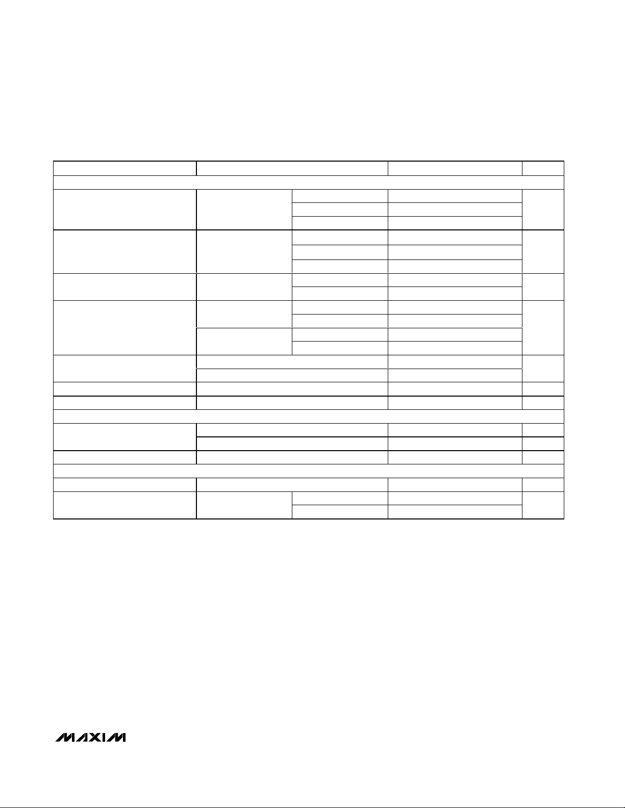
ELECTRICAL CHARACTERISTICS—V
OUT
= +2.5V
(VIN= +5V, I
OUT
= 0, TA= T
MIN
to T
MAX
. Typical values are at TA= +25°C, unless otherwise noted.) (Note 1)
OUTPUT
Output Voltage I
Output-Voltage Temperature
Coefficient (Note 2)
Line Regulation (Note 4) 4.5V < VIN < 40V
Load Regulation (Note 4)
OUT Short-Circuit Current
Thermal Hysteresis (Note 3) 150 ppm
Long-Term Stability ∆t = 1000hr 150 ppm
DYNAMIC CHARACTERISTICS
Output Noise Voltage
Turn-On Settling Time To V
INPUT
Supply Voltage Range Inferred from line regulation test 4.5 40.0 V
Quiescent Supply Current I
PARAMETER CONDITIONS MIN TYP MAX UNITS
= 0, TA = +25°C
OUT
= -40°C to +125°C
T
A
Sourcing,
0 < I
Sinking,
-0.6mA < I
Output shorted to GND 60
Output shorted to IN -2
0.1Hz to 10Hz 4 µV
10Hz to 1kHz 7 µV
< 10mA
OUT
< 0mA
OUT
= 0.05% of final value, C
OUT
= 0
OUT
MAX6043A (0.06%) 2.4985 2.5000 2.5015
MAX6043B (0.1%) 2.4975 2.5000 2.5025
MAX6043C (0.5%) 2.4876 2.5000 2.5125
MAX6043A_25 3 15
MAX6043B_25 5 25
MAX6043C_25 10 65
TA = +25°C16
T
= -40°C to +125°C 1.5 10
A
TA = +25°C870
T
= -40°C to +125°C70
A
TA = +25°C 70 900
T
= -40°C to +125°C 900
A
= 50pF 150 µs
OUT
TA = +25°C 320 490
= -40°C to +125°C 370 650
T
A
ppm/°C
ppm/V
ppm/mA
mA
V
P-P
RMS
µA
Page 3
MAX6043
Precision High-Voltage Reference in SOT23
_______________________________________________________________________________________ 3
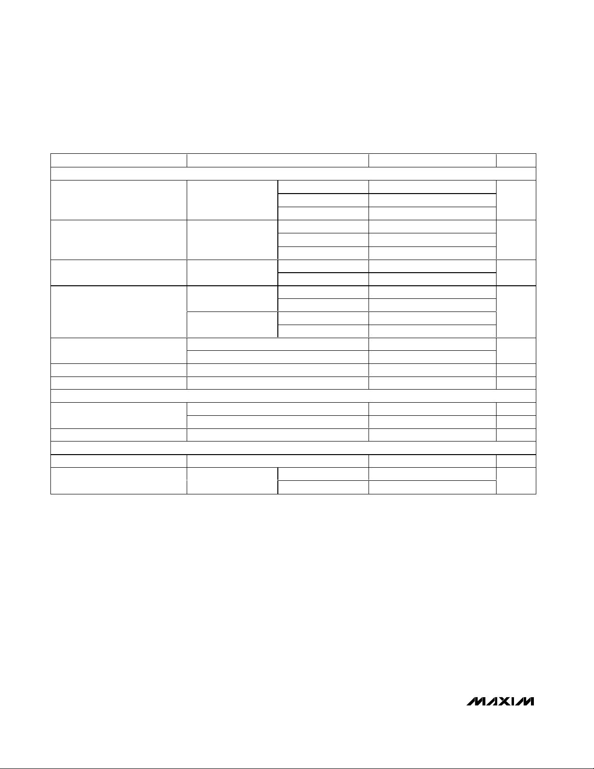
ELECTRICAL CHARACTERISTICS—V
OUT
= +3.3V
(VIN= +10V, I
OUT
= 0, TA= T
MIN
to T
MAX
. Typical values are at TA= +25°C, unless otherwise noted.) (Note 1)
OUTPUT
Output Voltage I
Output-Voltage Temperature
Coefficient (Note 2)
Line Regulation (Note 4) 5.3V ≤ VIN ≤ 40V
Load Regulation (Note 4)
OUT Short-Circuit Current
Thermal Hysteresis (Note 3) 150 ppm
Long-Term Stability ∆t = 1000hr 150 ppm
DYNAMIC CHARACTERISTICS
Output Noise Voltage
Turn-On Settling Time To V
INPUT
Supply Voltage Range Inferred from line regulation test 5.3 40.0 V
Quiescent Supply Current I
PARAMETER CONDITIONS MIN TYP MAX UNITS
= 0, TA = +25°C
OUT
T
= -40°C to +125°C
A
Sourcing,
0 ≤ I
Sinking,
-0.6mA ≤ I
OUT shorted to GND 60
OUT shorted to IN -2
0.1Hz to 10Hz 5.3 µV
10Hz to 1kHz 9.5 µV
≤ 10mA
OUT
≤ 0mA
OUT
= 0.05% of final value, C
OUT
= 0
OUT
MAX6043A (0.06%) 3.2980 3.3000 3.3020
MAX6043B (0.1%) 3.2967 3.3000 3.3033
MAX6043C (0.5%) 3.2836 3.3000 3.3165
MAX6043A_33 3 15
MAX6043B_33 5 25
MAX6043C_33 10 65
TA = +25°C16
= -40°C to +125°C 1.5 10
T
A
TA = +25°C2370
T
= -40°C to +125°C70
A
TA = +25°C 100 900
T
= -40°C to +125°C 900
A
= 50pF 180 µs
OUT
TA = +25°C 320 490
T
= -40°C to +125°C 380 650
A
ppm/°C
ppm/V
ppm/mA
mA
V
P-P
RMS
µA
Page 4
MAX6043
Precision High-Voltage Reference in SOT23
4 _______________________________________________________________________________________
ELECTRICAL CHARACTERISTICS—V
OUT
= +4.096V
(VIN= +10V, I
OUT
= 0, TA= T
MIN
to T
MAX
. Typical values are at TA= +25°C, unless otherwise noted.) (Note 1)
OUTPUT
Output-Voltage Temperature
Coefficient (Note 2)
Line Regulation (Note 4) 6.1V ≤ VIN ≤ 40V
Load Regulation (Note 4)
OUT Short-Circuit Current
Thermal Hysteresis (Note 3) 150 ppm
Long-Term Stability ∆t = 1000hr 150 ppm
DYNAMIC CHARACTERISTICS
Output Noise Voltage
Turn-On Settling Time To V
INPUT
Supply Voltage Range Inferred from line regulation test 6.1 40.0 V
Quiescent Supply Current I
PARAMETER CONDITIONS MIN TYP MAX UNITS
= 0, TA = +25°C
OUT
T
= -40°C to +125°C
A
Sourcing,
0 ≤ I
Sinking,
-0.6mA ≤ I
OUT shorted to GND 60
OUT shorted to IN -2
0.1Hz to 10Hz 6.6 µV
10Hz to 1kHz 12 µV
≤ 10mA
OUT
≤ 0mA
OUT
= 0.05% of final value, C
OUT
= 0
OUT
MAX6043A (0.06%) 4.0935 4.0960 4.0985
MAX6043B (0.1%) 4.0919 4.0960 4.1001Output Voltage I
MAX6043C (0.5%) 4.0755 4.0960 4.1165
MAX6043A_41 3 15
MAX6043B_41 5 25
MAX6043C_41 10 65
TA = +25°C16
= -40°C to +125°C 1.5 10
T
A
TA = +25°C1970
T
= -40°C to +125°C70
A
TA = +25°C 100 900
T
= -40°C to +125°C 900
A
= 50pF 200 µs
OUT
TA = +25°C 320 490
T
= -40°C to +125°C 380 650
A
V
ppm/°C
ppm/V
ppm/mA
mA
P-P
RMS
µA
Page 5
MAX6043
Precision High-Voltage Reference in SOT23
_______________________________________________________________________________________ 5
ELECTRICAL CHARACTERISTICS—V
OUT
= +5.0V
(VIN= +15V, I
OUT
= 0, TA= T
MIN
to T
MAX
. Typical values are at TA= +25°C, unless otherwise noted.) (Note 1)
OUTPUT
Output-Voltage Temperature
Coefficient (Note 2)
Line Regulation (Note 4) 7V ≤ VIN ≤ 40V
Load Regulation (Note 4)
OUT Short-Circuit Current
Thermal Hysteresis (Note 3) 150 ppm
Long-Term Stability ∆t = 1000hr 150 ppm
DYNAMIC CHARACTERISTICS
Output Noise Voltage
Turn-On Settling Time To V
INPUT
Supply Voltage Range Inferred from line regulation test 7.0 40.0 V
Quiescent Supply Current I
PARAMETER CONDITIONS MIN TYP MAX UNITS
= 0, TA = +25°C
OUT
T
= -40°C to +125°C
A
Sourcing,
0 ≤ I
Sinking,
-0.6mA ≤ I
OUT shorted to GND 60
OUT shorted to IN -2
0.1Hz to 10Hz 9.5 µV
10Hz to 1kHz 15 µV
≤ 10mA
OUT
≤ 0mA
OUT
= 0.05% of final value, C
OUT
= 0
OUT
MAX6043A (0.06%) 4.9970 5.0000 5.0030
MAX6043B (0.1%) 4.9950 5.0000 5.0050Output Voltage I
MAX6043C (0.5%) 4.9751 5.0000 5.0250
MAX6043A_50 3 15
MAX6043B_50 5 25
MAX6043C_50 10 65
TA = +25°C16
= -40°C to +125°C 1.5 10
T
A
TA = +25°C3270
T
= -40°C to +125°C70
A
TA = +25°C 130 900
T
= -40°C to +125°C 900
A
= 50pF 230 µs
OUT
TA = +25°C 320 490
= -40°C to +125°C 380 650
T
A
ppm/°C
ppm/V
ppm/mA
mA
V
P-P
RMS
µA
Page 6

MAX6043
Precision High-Voltage Reference in SOT23
6 _______________________________________________________________________________________
Note 1: All devices are 100% production tested at TA= +25°C and guaranteed by design over TA= T
MIN
to T
MAX
as specified.
Note 2: Temperature coefficient is defined as ∆V
OUT
divided by the temperature range.
Note 3: Thermal hysteresis defined as the change in output voltage at T
A
= +25°C before and after cycling the device from T
MAX
to T
MIN.
Note 4: Line and load regulation do not include the effect of self heating.
ELECTRICAL CHARACTERISTICS—V
OUT
= +10.0V
(VIN= +15V, I
OUT
= 0, TA= T
MIN
to T
MAX
. Typical values are at TA= +25°C, unless otherwise noted.) (Note 1)
OUTPUT
Output Voltage I
Output-Voltage Temperature
Coefficient (Note 2)
Line Regulation (Note 4) 12V ≤ VIN ≤ 40V
Load Regulation (Note 4)
OUT Short-Circuit Current
Thermal Hysteresis (Note 3) 150 ppm
Long-Term Stability ∆t = 1000hr 150 ppm
DYNAMIC CHARACTERISTICS
Output Noise Voltage
Turn-On Settling Time To V
INPUT
Supply Voltage Range Inferred from line regulation test 12.0 40.0 V
Quiescent Supply Current I
PARAMETER CONDITIONS MIN TYP MAX UNITS
= 0, TA = +25°C
OUT
T
= -40°C to +125°C
A
Sourcing,
0 ≤ I
Sinking,
-0.6mA ≤ I
OUT shorted to GND 60
OUT shorted to IN -2
0.1Hz to 10Hz 19 µV
10Hz to 1kHz 30 µV
≤ 10mA
OUT
≤ 0mA
OUT
= 0.05% of final value, C
OUT
= 0
OUT
MAX6043A (0.05%) 9.9950 10.0000 10.0050
MAX6043B (0.1%) 9.9900 10.0000 10.0100
MAX6043C (0.5%) 9.9500 10.0000 10.0500
MAX6043A_10 3 15
MAX6043B_10 5 25
MAX6043C_10 10 65
TA = +25°C16
= -40°C to +125°C 1.5 10
T
A
TA = +25°C1670
T
= -40°C to +125°C70
A
TA = +25°C 170 900
T
= -40°C to +125°C 900
A
= 50pF 390 µs
OUT
TA = +25°C 320 490
T
= -40°C to +125°C 390 650
A
V
ppm/°C
ppm/V
ppm/mA
mA
P-P
RMS
µA
Page 7

MAX6043
Precision High-Voltage Reference in SOT23
_______________________________________________________________________________________ 7
Typical Operating Characteristics
(VIN= +5V for V
OUT
= +2.5V, VIN= +10V for V
OUT
= +3.3V or +4.096V, VIN= +15V for V
OUT
= +5V or +10V, I
OUT
= 0, TA= +25°C,
unless otherwise noted.)
OUTPUT VOLTAGE (V)
OUTPUT VOLTAGE vs. TEMPERATURE
2.5020
THREE TYPICAL UNITS
2.5015
2.5010
2.5005
2.5000
2.4995
2.4990
2.4985
2.4980
-40 125
(V
OUT
TEMPERATURE (°C)
LOAD REGULATION
(SOURCING, V
2.0
1.5
1.0
(mV)
OUT
∆V
0.5
0
-0.5
-1.0
-1.5
-2.0
TA = -40°C
TA = +125°C
TA = +85°C
OUTPUT CURRENT (mA)
= 2.5V)
= 2.5V)
OUT
OUTPUT VOLTAGE vs. TEMPERATURE
10.005
THREE TYPICAL UNITS
10.004
10.003
MAX6043 toc01
10.002
10.001
10.000
9.999
9.998
9.997
9.996
9.995
OUTPUT VOLTAGE (V)
9.994
9.993
9.992
9.991
9.990
1109565 80-10 5 20 35 50-25
MAX6043 toc04
TA = +25°C
605010 20 30 40070
-40 125
25
20
15
10
(mV)
5
OUT
∆V
0
-5
-10
TA = +125°C
-15
-4 0
= 10V)
(V
OUT
TEMPERATURE (°C)
LOAD REGULATION
(SINKING, V
OUTPUT CURRENT (mA)
OUT
TA = +85°C
= 10V)
TA = +25°C
TA = -40°C
-1-2-3
(SOURCING, V
4
2
MAX6043 toc02
0
-2
-4
(mV)
OUT
-6
∆V
-8
-10
TA = +125°C
-12
1109565 80-10 5 20 35 50-25
-14
TA = +85°C
070
(SINKING, V
2.0
1.5
MAX6043 toc05
1.0
0.5
(mV)
0
OUT
∆V
-0.5
-1.0
TA = +125°C
-1.5
-2.0
-3.0 0
LOAD REGULATION
= 10V)
OUT
TA = +25°C
OUTPUT CURRENT (mA)
TA = -40°C
LOAD REGULATION
= 2.5V)
OUT
TA = +25°C
TA = -40°C
TA = +85°C
OUTPUT CURRENT (mA)
MAX6043 toc03
605030 402010
MAX6043 toc06
-0.5-1.0-2.5 -2.0 -1.5
0.1750
0.1500
0.1250
0.1000
0.0750
(mV)
OUT
0.0500
∆V
0.0250
-0.0250
-0.0500
0
LINE REGULATION
TA = +125°C
TA = +85°C
= 2.5V)
(V
OUT
TA = -40°C
INPUT VOLTAGE (V)
0.500
0.400
MAX6043 toc07
0.300
0.200
(mV)
OUT
0.100
∆V
TA = +25°C
-0.100
363224 2812 16 208440
-0.200
TA = -40°C
0
TA = +85°C
LINE REGULATION
= 10V)
(V
OUT
TA = +125°C
TA = +25°C
INPUT VOLTAGE (V)
MAX6043 toc08
363216 20 24 2812 40
MINIMUM INPUT-OUTPUT DIFFERENTIAL
vs. LOAD CURRENT (V
3.0
V
∆
/ V
= 0.1%
OUT
OUT
2.5
TA = -40°C
2.0
1.5
1.0
0.5
MINIMUM INPUT-OUTPUT DIFFERENTIAL (V)
0
080
TA = +125°C
LOAD CURRENT (mA)
= 2.5V)
OUT
TA = +85°C
604020
TA = +25°C
MAX6043 toc09
Page 8

MAX6043
Precision High-Voltage Reference in SOT23
8 _______________________________________________________________________________________
Typical Operating Characteristics (continued)
(VIN= +5V for V
OUT
= +2.5V, VIN= +10V for V
OUT
= +3.3V or +4.096V, VIN= +15V for V
OUT
= +5V or +10V, I
OUT
= 0, TA= +25°C,
unless otherwise noted.)
MINIMUM INPUT-OUTPUT DIFFERENTIAL
vs. LOAD CURRENT (V
OUT
= 10V)
MAX6043 toc10
LOAD CURRENT (mA)
MINIMUM INPUT-OUTPUT DIFFERENTIAL (V)
4020
0.5
1.0
1.5
2.0
2.5
3.0
0
060
∆
V
OUT
/ V
OUT
= 0.1%
TA = +125°C
TA = +85°C
TA = +25°C
TA = -40°C
POWER-SUPPLY REJECTION RATIO
vs. FREQUENCY (V
OUT
= 2.5V)
MAX6043 toc11
FREQUENCY (kHz)
PSRR (dB)
100101
-100
-80
-60
-40
-20
0
-120
0.1 1000
POWER-SUPPLY REJECTION RATIO
vs. FREQUENCY (V
OUT
= 10V)
MAX6043 toc12
FREQUENCY (kHz)
PSRR (dB)
100101
-100
-80
-60
-40
-20
0
-120
0.1 1000
0.1 1 100 1000
OUTPUT IMPEDANCE
vs. FREQUENCY
MAX6043 toc13
FREQUENCY (kHz)
OUTPUT IMPEDANCE (Ω)
10
100
0.01
0.1
1
10
SUPPLY CURRENT vs. INPUT VOLTAGE
(V
OUT
= 2.5V)
MAX6043 toc14
INPUT VOLTAGE (V)
SUPPLY CURRENT (µA)
363224 288 12 16 204
40
80
120
160
200
240
280
320
360
400
440
480
0
040
TA = +125°C
TA = +85°C
TA = -40°C
TA = +25°C
SUPPLY CURRENT vs. INPUT VOLTAGE
(V
OUT
= 10V)
MAX6043 toc15
INPUT VOLTAGE (V)
SUPPLY CURRENT (µA)
363224 288 12 16 204
40
80
120
160
200
240
280
320
360
400
440
0
040
TA = +125°C
TA = +85°C
TA = -40°C
TA = +25°C
SUPPLY CURRENT vs. TEMPERATURE
(V
OUT
= 2.5V)
MAX6043 toc16
TEMPERATURE (°C)
SUPPLY CURRENT (µA)
1109565 80-10 5 20 35 50-25
260
280
300
320
340
360
380
400
420
440
240
-40 125
VIN = 5V
SUPPLY CURRENT vs. TEMPERATURE
(V
OUT
= 10V)
MAX6043 toc17
TEMPERATURE (°C)
SUPPLY CURRENT (µA)
1109565 80-10 5 20 35 50-25
260
280
300
320
340
360
380
400
420
440
240
-40 125
VIN = 15V
OUTPUT NOISE-VOLTAGE DENSITY
vs. FREQUENCY
MAX6043 toc18
FREQUENCY (Hz)
OUTPUT NOISE-VOLTAGE DENSITY (nV/√Hz)
100101
1000
0.1 1000
10,000
100
V
OUT
= 10V
V
OUT
= 2.5V
Page 9

MAX6043
Precision High-Voltage Reference in SOT23
_______________________________________________________________________________________ 9
Typical Operating Characteristics (continued)
(VIN= +5V for V
OUT
= +2.5V, VIN= +10V for V
OUT
= +3.3V or +4.096V, VIN= +15V for V
OUT
= +5V or +10V, I
OUT
= 0, TA= +25°C,
unless otherwise noted.)
2.5V
0.1Hz TO 10Hz OUTPUT NOISE
= 2.5V)
(V
OUT
1s/div
LOAD TRANSIENT
= 2.5V)
(V
OUT
VIN = 5V
= 0µF
C
OUT
0.1Hz TO 10Hz OUTPUT NOISE
MAX6043 toc19
V
OUT
AC-COUPLED
1µV/div
MAX6043 toc21
VIN = 15V
= 0µF
C
V
OUT
50mV/div
AC-COUPLED
OUT
10V
(V
OUT
1s/div
LOAD TRANSIENT
(V
OUT
= 10V)
= 10V)
MAX6043 toc20
MAX6043 toc22
V
OUT
AC-COUPLED
4µV/div
V
OUT
200mV/div
AC-COUPLED
20mA
2.5V
20mA
I
OUT
10mA/div
0
100µs/div
LOAD TRANSIENT
= 2.5V)
(V
OUT
VIN = 5V
= 1µF
C
OUT
0
100µs/div
MAX6043 toc23
V
OUT
50mV/div
AC-COUPLED
I
OUT
10mA/div
20mA
10V
20mA
I
OUT
10mA/div
0
100µs/div
LOAD TRANSIENT
= 10V)
(V
OUT
0
100µs/div
MAX6043 toc24
VIN = 15V
= 1µF
C
OUT
V
OUT
100mV/div
AC-COUPLED
I
OUT
10mA/div
Page 10

TURN-ON TRANSIENT
(V
OUT
= 2.5V)
MAX6043 toc31
C
OUT
= 0µF
0V
2.5V
5V
V
IN
2V/div
V
OUT
1V/div
4µs/div
0V
TURN-ON TRANSIENT
(V
OUT
= 10V)
MAX6043 toc32
C
OUT
= 0µF
0V
10V
15V
V
IN
5V/div
V
OUT
5V/div
40µs/div
0V
MAX6043
Precision High-Voltage Reference in SOT23
10 ______________________________________________________________________________________
Typical Operating Characteristics (continued)
(VIN= +5V for V
OUT
= +2.5V, VIN= +10V for V
OUT
= +3.3V or +4.096V, VIN= +15V for V
OUT
= +5V or +10V, I
OUT
= 0, TA= +25°C,
unless otherwise noted.)
LOAD TRANSIENT
(V
OUT
= 2.5V)
MAX6043 toc25
VIN = 5V
C
OUT
= 0µF
-2mA
0
2.5V
V
OUT
50mV/div
AC-COUPLED
I
OUT
2mA/div
200µs/div
LOAD TRANSIENT
(V
OUT
= 10V)
MAX6043 toc26
VIN = 15V
C
OUT
= 0µF
-2mA
0
10V
V
OUT
100mV/div
AC-COUPLED
I
OUT
2mA/div
400µs/div
LINE TRANSIENT
(V
OUT
= 2.5V)
MAX6043 toc29
V
IN
AC-COUPLED
500mV/div
10µs/div
5.5V
V
OUT
AC-COUPLED
10mV/div
4.5V
LINE TRANSIENT
(V
OUT
= 10V)
MAX6043 toc30
V
IN
AC-COUPLED
500mV/div
10µs/div
15.5V
V
OUT
AC-COUPLED
10mV/div
14.5V
LOAD TRANSIENT
(V
OUT
= 2.5V)
MAX6043 toc27
VIN = 5V
C
OUT
= 1µF
-2mA
0
2.5V
V
OUT
20mV/div
AC-COUPLED
I
OUT
2mA/div
200µs/div
LOAD TRANSIENT
(V
OUT
= 10V)
MAX6043 toc28
VIN = 15V
C
OUT
= 1µF
-2mA
0
10V
V
OUT
50mV/div
AC-COUPLED
I
OUT
2mA/div
400µs/div
Page 11

MAX6043
Precision High-Voltage Reference in SOT23
______________________________________________________________________________________ 11
Typical Operating Characteristics (continued)
(VIN= +5V for V
OUT
= +2.5V, VIN= +10V for V
OUT
= +3.3V or +4.096V, VIN= +15V for V
OUT
= +5V or +10V, I
OUT
= 0, TA= +25°C,
unless otherwise noted.)
TURN-OFF TRANSIENT
(V
OUT
= 10V)
MAX6043 toc36
C
OUT
= 0µF
0V
10V
15V
V
IN
5V/div
V
OUT
5V/div
2µs/div
0V
TURN-OFF TRANSIENT
(V
OUT
= 2.5V)
MAX6043 toc37
C
OUT
= 1µF
0V
2.5V
5V
V
IN
2V/div
V
OUT
1V/div
20ms/div
0V
LONG-TERM DRIFT
(V
OUT
= 10V)
XMAX6043 toc40
TIME (hr)
∆ OUTPUT VOLTAGE (ppm)
800600400200
-125
-75
-100
-50
-25
0
50
25
75
100
125
150
-150
0 1000
5V
0V
2.5V
0V
TURN-ON TRANSIENT
C
= 1µF
OUT
= 2.5V)
(V
OUT
40µs/div
MAX6043 toc33
V
IN
2V/div
V
OUT
1V/div
TURN-ON TRANSIENT
= 10V)
(V
15V
10V
OUT
C
= 1µF
OUT
0V
0V
40µs/div
MAX6043 toc34
V
5V/div
V
5V/div
IN
OUT
5V
0V
2.5V
0V
15V
TURN-OFF TRANSIENT
(V
OUT
C
= 0µF
OUT
TURN-OFF TRANSIENT
C
= 1µF
OUT
= 2.5V)
1µs/div
MAX6043 toc35
MAX6043 toc38
V
IN
2V/div
V
OUT
1V/div
V
IN
5V/div
LONG-TERM DRIFT
= 2.5V)
(V
150
125
100
75
50
25
0
-25
-50
∆ OUTPUT VOLTAGE (ppm)
-75
-100
-125
-150
0 1000
OUT
TIME (hr)
0V
10V
V
OUT
0V
40ms/div
MAX6043 toc39
800600400200
5V/div
Page 12

MAX6043
Precision High-Voltage Reference in SOT23
12 ______________________________________________________________________________________
Applications Information
Bypassing/Output Capacitance
For the best line-transient performance, decouple the
input with a 0.1µF ceramic capacitor as shown in the
Typical Operating Circuit. Place the capacitor as close
to IN as possible. When transient performance is less
important, no capacitor is necessary.
The MAX6043 does not require an output capacitor for
stability and is stable with capacitive loads up to 100µF.
In applications where the load or the supply can experience step changes, a larger output capacitor reduces
the amount of overshoot (undershoot) and improves the
circuit’s transient response. Place output capacitors as
close to the device as possible for best performance.
Supply Current
The MAX6043 consumes 320µA of quiescent supply
current. This improved efficiency reduces power dissipation and extends battery life.
Thermal Hysteresis
Thermal hysteresis is the change in the output voltage
at TA= +25°C before and after the device is cycled
over its entire operating temperature range. Hysteresis
is caused by differential package stress appearing
across the bandgap core transistors. The typical thermal hysteresis value is 150ppm.
Turn-On Time
The MAX6043 typically turns on and settles to within
0.05% of the preset output voltage in 150µs.
Short-Circuited Outputs
The MAX6043 features a short-circuit-protected output.
Internal circuitry limits the output current to 60mA when
short-circuiting the output.
Temperature Coefficient vs.
Operating Temperature Range
for a 1 LSB Maximum Error
In a data converter application, the reference voltage of
the converter must stay within a certain limit to keep the
error in the data converter smaller than the resolution
limit through the operating temperature range. Figure 1
shows the maximum allowable reference-voltage temperature coefficient to keep the conversion error to less
than 1 LSB, as a function of the operating temperature
range (T
MAX
- T
MIN
) with the converter resolution as a
parameter. The graph assumes the reference-voltage
temperature coefficient as the only parameter affecting
accuracy.
In reality, the absolute static accuracy of a data converter is dependent on the combination of many parameters
such as integral nonlinearity, differential nonlinearity,
offset error, gain error, as well as voltage-reference
changes.
Pin Description
PIN NAME FUNCTION
1, 3 I.C. Internally Connected. Do not connect externally.
2 GND Ground
4 IN Positive Power-Supply Input
5 OUTF
6 OUTS Voltage-Reference Sense Input
Voltage-Reference Force Output. Connect OUTF to OUTS as close to the device as possible. OUTF
and OUTS do not require a bypass capacitor for stability.
Page 13

MAX6043
Precision High-Voltage Reference in SOT23
______________________________________________________________________________________ 13
Figure 1. Temperature Coefficient vs. Operating Temperature Range for a 1 LSB Maximum Error
10,000
1000
100
TEMPERATURE
COEFFICIENT
(ppm/°C)
10
1
0.1
0.01
110
OPERATING TEMPERATURE RANGE (T
MAX
- T
MIN
) (°C)
8 BIT
10 BIT
12 BIT
14 BIT
16 BIT
18 BIT
20 BIT
100
Page 14

MAX6043
Precision High-Voltage Reference in SOT23
14 ______________________________________________________________________________________
Ordering Information (continued)
Chip Information
TRANSISTOR COUNT: 152
PROCESS: BiCMOS
*INPUT CAPACITOR IS OPTIONAL.
IN
GND
INPUT
SUPPLY
REFERENCE
OUTPUT
(SEE ORDERING
INFORMATION)
0.1µF
*
MAX6043
OUTF
OUTS
Typical Operating Circuit
PART TEMP RANGE
MAX6043AAUT33-T -40°C to +125°C 6 SOT23-6 ABSA
MAX6043BAUT33-T -40°C to +125°C 6 SOT23-6 ABDS
MAX6043CAUT33-T -40°C to +125°C 6 SOT23-6 ABDT
MAX6043AAUT41-T -40°C to +125°C 6 SOT23-6 ABSB
MAX6043BAUT41-T -40°C to +125°C 6 SOT23-6 ABDU
MAX6043CAUT41-T -40°C to +125°C 6 SOT23-6 ABDV
MAX6043AAUT50-T -40°C to +125°C 6 SOT23-6 ABSC
MAX6043BAUT50-T -40°C to +125°C 6 SOT23-6 ABDW
MAX6043CAUT50-T -40°C to +125°C 6 SOT23-6 ABDX
MAX6043AAUT10-T -40°C to +125°C 6 SOT23-6 ABSD
MAX6043BAUT10-T -40°C to +125°C 6 SOT23-6 ABDY
MAX6043CAUT10-T -40°C to +125°C 6 SOT23-6 ABDZ
PINPACKAGE
TOP
MARK
Page 15

MAX6043
Precision High-Voltage Reference in SOT23
Maxim cannot assume responsibility for use of any circuitry other than circuitry entirely embodied in a Maxim product. No circuit patent licenses are
implied. Maxim reserves the right to change the circuitry and specifications without notice at any time.
Maxim Integrated Products, 120 San Gabriel Drive, Sunnyvale, CA 94086 408-737-7600 ____________________ 15
© 2004 Maxim Integrated Products Printed USA is a registered trademark of Maxim Integrated Products.
Package Information
(The package drawing(s) in this data sheet may not reflect the most current specifications. For the latest package outline information,
go to www.maxim-ic.com/packages
.)
6LSOT.EPS
PACKAGE OUTLINE, SOT-23, 6L
1
21-0058
F
1
 Loading...