

Page 1
General Description
The MAX6035 is a high-voltage, precision micropower
voltage reference. This three-terminal device is available
with output voltage options of 2.5V, 3.0V, and 5.0V. It is an
excellent upgrade for industry-standard devices such as
the REF02 and REF43. The MAX6035 offers 14x lower
power than the REF02 and 5x lower power than the
REF43, as well as a reduced package size from an 8-pin
SO to a 3-pin SOT23. The MAX6035 features a proprietary
temperature coefficient curvature-correction circuit and
laser-trimmed, thin-film resistors that result in a very low
temperature coefficient of 25ppm/°C (max) and an initial
accuracy of ±0.2% (max).
The MAX6035 typically draws only 73µA of supply current and can source 10mA or sink 2mA of load current.
Unlike conventional shunt-mode (two-terminal) references that waste supply current and require an external
resistor, this device offers a supply current that is virtually independent of the supply voltage and does not
require an external resistor. Additionally, this internally
compensated device does not require an external compensation capacitor, but is also stable with capacitive
loads up to 5µF. Eliminating the external compensation
capacitor saves valuable board area in space-critical
applications. The supply independent, ultra-low supply
current makes this device ideal for battery-operated,
high-performance systems.
The MAX6035 is available in a 3-pin SOT23 package
and is specified for operation from -40°C to +125°C.
Applications
Features
♦ Wide Supply Voltage Range: Up to 33V
♦ 25ppm/°C (max) Temperature Coefficient
(-40°C to +85°C)
♦ ±0.2% (max) Initial Accuracy
♦ 95µA (max) Quiescent Supply Current
♦ 10mA Source Current, 2mA Sink Current
♦ No Output Capacitor Required
♦ Stable with Capacitive Loads up to 5µF
MAX6035
High-Supply-Voltage, Precision
Voltage Reference in SOT23
________________________________________________________________ Maxim Integrated Products 1
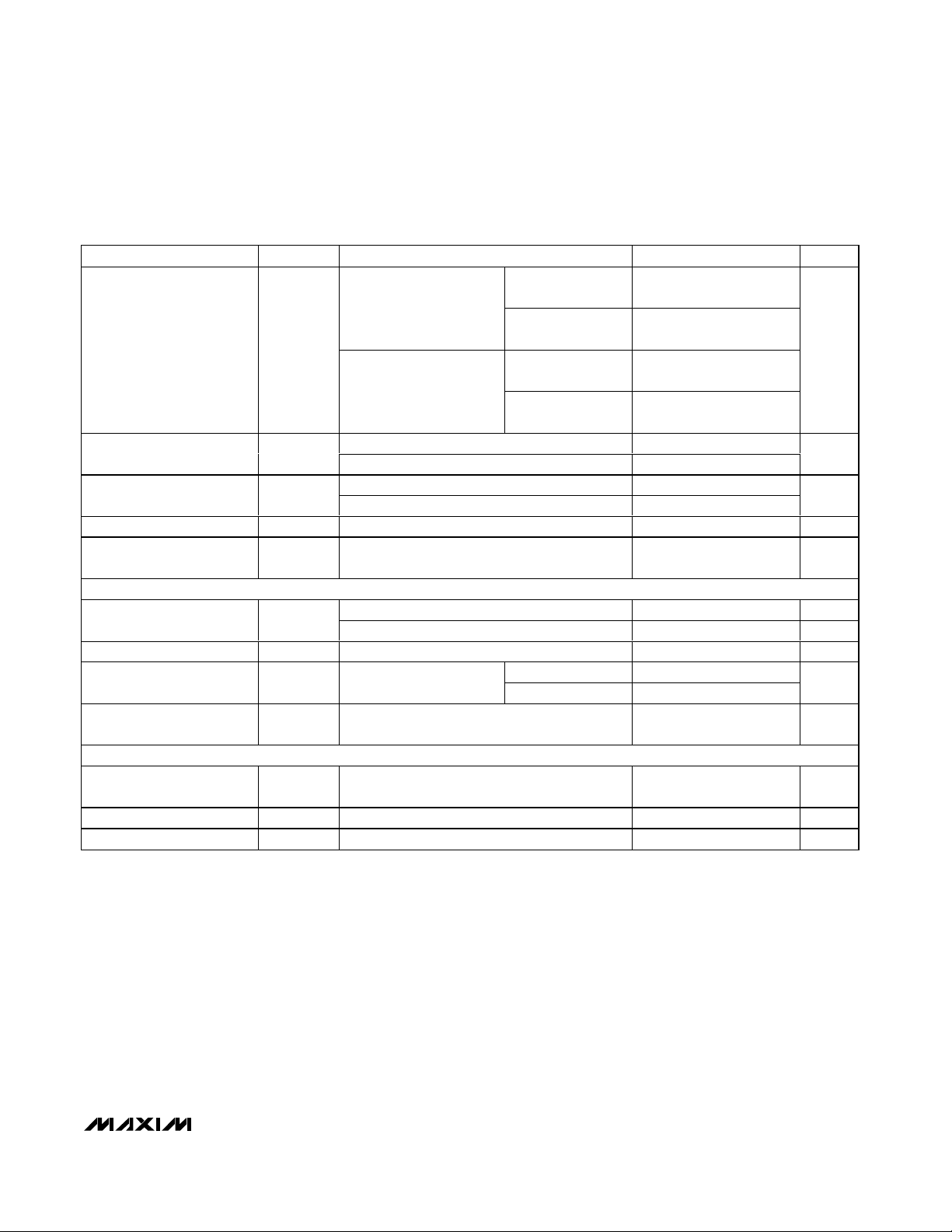
Ordering Information
19-2606; Rev 3; 11/06
For pricing, delivery, and ordering information, please contact Maxim/Dallas Direct! at
1-888-629-4642, or visit Maxim’s website at www.maxim-ic.com.
PART
TEMP RANGE
PIN -
TOP
MARK
MAX6035AAUR25-T
FZMW
MAX6035BAUR25-T
FZMX
MAX6035ESA25
8 SO —
MAX6035AAUR30-T
FZMY
MAX6035BAUR30-T
FZMZ
MAX6035AAUR50-T
FZNA
MAX6035BAUR50-T
FZNB
(
)
Selector Guide
OUT
1
3 GND
IN
MAX6035
SOT23
TOP VIEW
2
OUT
N.C.GND
1
2
87N.C.
N.C.IN
N.C.
N.C.
SO
3
4
6
5
MAX6035
Pin Configurations
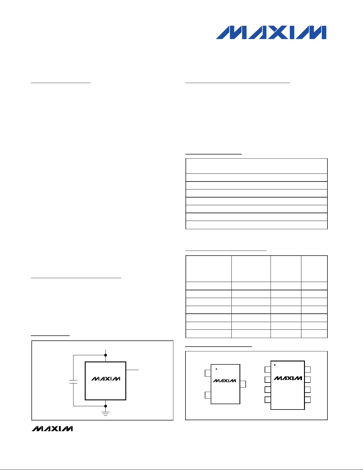
MAX6035
0.1µF*
*CAPACITOR IS OPTIONAL.
REFERENCE
OUT
OUT
IN
GND
+SUPPLY INPUT (SEE SELECTOR GUIDE)
Typical Operating Circuit
4mA to 20mA Industrial
Control Loops
Li+ Battery Chargers
12-Bit A/D and D/A
Converters
Digital Multimeters
Portable Data-Acquisition
Systems
Low-Power Test
Equipment
Note: The 3-pin SOT23 package code is U3-1. The 8-pin SO
package code is S8-2.
PA C K A G E
-40°C to +125°C 3 SOT23-3
-40°C to +125°C 3 SOT23-3
-40°C to +85°C
-40°C to +125°C 3 SOT23-3
-40°C to +125°C 3 SOT23-3
-40°C to +125°C 3 SOT23-3
-40°C to +125°C 3 SOT23-3
MAXIMUM
PART
MAX6035AAUR25 25 0.20 2.5
MAX6035BAUR25 65 0.50 2.5
MAX6035ESA25 40 0.20 2.5
MAX6035AAUR30 25 0.20 3.0
MAX6035BAUR30 65 0.50 3.0
MAX6035AAUR50 25 0.20 5.0
MAX6035BAUR50 65 0.50 5.0
TEMPCO
(ppm/°C)
-40°C to +85°C
MAXIMUM
INITIAL
ACCURACY
(%)
OUTPUT
VOLTAGE
(V)
Page 2
MAX6035
High-Supply-Voltage, Precision
Voltage Reference in SOT23
2 _______________________________________________________________________________________
ABSOLUTE MAXIMUM RATINGS
ELECTRICAL CHARACTERISTICS—MAX6035_AUR25 and MAX6035ESA25 (2.5V)
(VIN= 5V, I
OUT
= 0, TA= T
MIN
to T
MAX
, unless otherwise noted. Typical values are at TA= +25°C.) (Note 2)
Stresses beyond those listed under “Absolute Maximum Ratings” may cause permanent damage to the device. These are stress ratings only, and functional
operation of the device at these or any other conditions beyond those indicated in the operational sections of the specifications is not implied. Exposure to
absolute maximum rating conditions for extended periods may affect device reliability.
(Voltages referenced to GND)
IN ............................................................................-0.3V to +36V
OUT .............................................................-0.3V to (V
IN
+ 0.3V)
OUT Short-Circuit Duration to GND or IN (Note 1).....Continuous
Current into Any Pin..........................................................±20mA
Continuous Power Dissipation
3-Pin SOT23 (derate 4.0mW/°C above +70°C)............320mW
8-Pin SO (derate 5.9mW/°C above +70°C)...............470.6mW
Operating Temperature Range:
MAX6035ESA ..................................................-40°C to +85°C
MAX6035_AUR ..............................................-40°C to +125°C
Storage Temperature Range .............................-65°C to +150°C
Junction Temperature......................................................+150°C
Lead Temperature (soldering, 10s) .................................+300°C
PARAMETER
CONDITIONS
UNITS
MAX6035AAUR,
Output Voltage V
OUT
TA = +25°C
MAX6035BAUR
V
MAX6035AAUR 20
TA = 0°C to +70°C
MAX6035BAUR 50
MAX6035AAUR 25
MAX6035ESA 40
TA = -40°C to +85°C
MAX6035BAUR 65
MAX6035AAUR 30
Output Voltage
Temperature Coefficient
(Notes 3 and 6)
TCV
OUT
TA = -40°C to +125°C
MAX6035BAUR 75
ppm/°C
TA = +25°C415
Line Regulation (Note 4)
TA = T
MIN
to T
MAX
20
µV/V
Sourcing:
0 ≤ I
OUT
≤ 10mA
25 70
TA = +25°C,
MAX6035_AUR
Sinking:
-2mA ≤ I
OUT
≤ 0
45 180
Sourcing:
0 ≤ I
OUT
≤ 10mA
85
TA = T
MIN
to T
MAX
,
MAX6035_AUR
Sinking:
-2mA ≤ I
OUT
≤ 0
225
Sourcing:
0 ≤ I
OUT
≤ 10mA
105 175
TA = +25°C,
MAX6035ESA
Sinking:
-2mA ≤ I
OUT
≤ 0
205 375
Sourcing:
0 ≤ I
OUT
≤ 10mA
350
Load Regulation (Note 4)
∆V
OUT
/
∆I
OUT
TA = T
MIN
to T
MAX
,
MAX6035ESA
Sinking:
-2mA ≤ I
OUT
≤ 0
500
µV/mA
Short to GND 27
OUT Short-Circuit Current I
SC
Short to IN -4
mA
Note 1: Continuous power dissipation should also be observed.
SYMBOL
MIN TYP MAX
MAX6035ESA (0.2%)
∆V
/∆VIN(V
OUT
OUT
+ 2V) ≤ VIN ≤ 33V
2.4950 2.5000 2.5050
2.4875 2.5000 2.5125
Page 3
MAX6035
High-Supply-Voltage, Precision
Voltage Reference in SOT23
_______________________________________________________________________________________ 3
PARAMETER
SYMBOL
CONDITIONS
MIN
TYP
MAX
UNITS
I
OUT
= 10µA 1.9
Dropout Voltage (Note 7)
I
OUT
= 10mA
V
Thermal Hysteresis (Note 5)
135
ppm
Long-Term Stability
1000hr at +25°C 110
ppm/
1000hr
DYNAMIC CHARACTERISTICS
f = 0.1Hz to 10Hz 21
µV
P-P
Output Noise Voltage e
n
f = 10Hz to 1kHz 20
µV
RMS
Ripple Rejection
VIN = 5V ±100mV, f = 120Hz 86 dB
C
OUT
= 50pF 35
Turn-On Settling Time t
R
To V
OUT
= 0.1%
of final value
C
OUT
= 1µF 240
µs
Capacitive-Load Stability
(Note 6)
C
OUT
05µF
INPUT CHARACTERISTICS
Supply Voltage Range V
IN
Infer r ed fr om l i ne r eg ul ati on and d r op out vol tag e 4.4 33 V
Quiescent Supply Current I
IN
73 95 µA
Change in Supply Current
4.4V ≤ VIN ≤ 33V 0.4 0.7
µA/V
ELECTRICAL CHARACTERISTICS—MAX6035_AUR25 and MAX6035ESA25 (2.5V)
(continued)
(VIN= 5V, I
OUT
= 0, TA= T
MIN
to T
MAX
, unless otherwise noted. Typical values are at TA= +25°C.) (Note 2)
PARAMETER
SYMBOL
CONDITIONS
MIN
TYP
MAX
UNITS
Output Voltage V
OUT
TA = +25°C
V
MAX6035A 20
TA = 0°C to +70°C
MAX6035B 50
MAX6035A 25
TA = -40°C to +85°C
MAX6035B 65
MAX6035A 30
Output Voltage
Temperature Coefficient
(Note 3)
TCV
OUT
TA = -40°C to +125°C
MAX6035B 75
ppm/°C
TA = +25°C 4.5 15
24
Line Regulation (Note 4)
∆V
OUT
/
∆V
IN
(V
OUT
+ 2V) ≤ VIN ≤ 33V
24
µV/V
Sourcing:
0 ≤ I
OUT
≤ 10mA
30 81
TA = +25°C
Sinking:
54 170
Sourcing:
0 ≤ I
OUT
≤ 10mA
96
Load Regulation (Note 4)
∆V
OUT
/
∆I
OUT
TA = -40°C to +125°C
Sinking:
230
µV/mA
ELECTRICAL CHARACTERISTICS—MAX6035_AUR30 (3.0V)
(VIN= 5V, I
OUT
= 0, TA= T
MIN
to T
MAX
, unless otherwise noted. Typical values are at TA= +25°C.) (Note 2)
VIN - V
OUT
∆V
/cycl e
OU T
∆V
/time
OUT
∆V
/∆V
OUT
IN
∆IIN/∆V
IN
2.25
MAX6035A (0.2%) 2.9940 3.0000 3.0060
MAX6035B (0.5%) 2.9850 3.0000 3.0150
( V
+ 1.75V ) ≤ V
OU T
≤ 33V
I N
= 0°C to +125°C
T
A
TA = -40°C to +125°C
-2mA ≤ I
-2mA ≤ I
≤ 0mA
OUT
≤ 0mA
OUT
Page 4
MAX6035
High-Supply-Voltage, Precision
Voltage Reference in SOT23
4 _______________________________________________________________________________________
PARAMETER
SYMBOL
CONDITIONS
MIN
TYP
MAX
UNITS
Short to GND 27
OUT Short-Circuit Current I
SC
Short to IN -4
mA
TA = 0°C to +125°CI
OUT
= 10µA
I
OUT
= 10µA 1.9Dropout Voltage (Note 7)
TA = -40°C to +125°C
I
OUT
= 10mA
V
Thermal Hysteresis (Note 5)
135
ppm
Long-Term Stability
1000hr at +25°C 120
ppm/
1000hr
DYNAMIC CHARACTERISTICS
f = 0.1Hz to 10Hz 25
µV
P-P
Output Noise Voltage e
n
f = 10Hz to 1kHz 25
µV
RMS
Ripple Rejection
∆V
OUT
/
∆V
IN
V
IN
= 5V ±100mV, f = 120Hz 80 dB
C
OUT
= 50pF 40
Turn-On Settling Time t
R
V
OUT
= 0.1% of final value
C
OUT
= 1µF 250
µs
Capacitive-Load Stability
(Note 6)
C
OUT
05µF
INPUT CHARACTERISTICS
TA = 0°C to +125°C, inferred from line regulation
and dropout voltage
33
Supply Voltage Range V
IN
TA = -40°C to +125°C, inferred from line
regulation and dropout voltage
4.9 33
V
Quiescent Current Supply I
IN
73 95 µA
Change in Supply Current
4.9V ≤ VIN ≤ 33V 0.4 0.7 µA/V
ELECTRICAL CHARACTERISTICS—MAX6035_AUR30 (3.0V) (continued)
(VIN= 5V, I
OUT
= 0, TA= T
MIN
to T
MAX
, unless otherwise noted. Typical values are at TA= +25°C.) (Note 2)
ELECTRICAL CHARACTERISTICS—MAX6035_AUR50 (5.0V)
(VIN= 5V, I
OUT
= 0, TA= T
MIN
to T
MAX
, unless otherwise noted. Typical values are at TA= +25°C.) (Note 2)
PARAMETER
CONDITIONS
UNITS
Output Voltage V
OUT
TA = +25°C
V
MAX6035A 20
TA = 0°C to +70°C
MAX6035B 50
MAX6035A 25
TA = -40°C to +85°C
MAX6035B 65
MAX6035A 30
Output Voltage
Temperature Coefficient
(Note 3)
TCV
OUT
TA = -40°C to +125°C
MAX6035B 75
ppm/°C
TA = + 25°C 7.5 25
Line Regulation (Note 4)
840
µV/V
VIN - V
OUT
∆V
/cycl e
OU T
∆V
/time
OUT
1.75
2.25
4.75
∆IIN/∆V
∆V
IN
SYMBOL
MAX6035A (0.2%) 4.9900 5.0000 5.0100
MAX6035B (0.5%) 4.9750 5.0000 5.0250
/∆VIN(V
OUT
OUT
+ 2V) ≤ V
≤ 33V
OUT
= - 40°C to + 125°C
T
A
MIN TYP MAX
Page 5
MAX6035
High-Supply-Voltage, Precision
Voltage Reference in SOT23
_______________________________________________________________________________________ 5
ELECTRICAL CHARACTERISTICS—MAX6035_AUR50 (5.0V) (continued)
(VIN= 5V, I
OUT
= 0, TA= T
MIN
to T
MAX
, unless otherwise noted. Typical values are at TA= +25°C.) (Note 2)
PARAMETER
CONDITIONS
UNITS
Sourcing:
0 ≤ I
OUT
≤ 10mA
50 135
TA = +25°C
Sinking:
90 215
Sourcing:
0 ≤ I
OUT
≤ 10mA
160
Load Regulation (Note 4)
∆V
OUT
/
∆I
OUT
TA = -40°C to +125°C
Sinking:
300
µV/mA
Shorted to GND 27
OUT Short-Circuit Current I
SC
Shorted to IN -4
mA
I
OUT
= 10µA 1.9
Dropout Voltage (Note 7)
I
OUT
= 10mA
V
Thermal Hysteresis (Note 5)
ppm
Long-Term Stability
1000hr at +25°C
ppm/
1000hr
DYNAMIC CHARACTERISTICS
f = 0.1Hz to 10Hz 68
µV
P-P
Output Noise Voltage e
n
f = 10Hz to 1kHz 48
µV
RMS
Ripple Rejection
VIN = 15V ±100mV, f = 120Hz 72 dB
C
OUT
= 50pF
Turn-On Settling Time t
R
To V
OUT
= 0.1% of final
value
C
OUT
= 1µF
µs
Capacitive-Load Stability
(Note 6)
C
OUT
05µF
INPUT CHARACTERISTICS
Supply Voltage Range V
IN
Inferred by line regulation and dropout voltage 6.9 33 V
Quiescent Current Supply I
IN
80 100 µA
Change in Supply Current
6.9V ≤ VIN ≤ 33V 0.4 0.7
µA/V
Note 2: All devices are 100% production tested at TA= +25°C and are guaranteed by design for TA= T
MIN
to T
MAX
, as specified.
Note 3: Temperature Coefficient is measured by the “box” method, i.e., the maximum ∆V
OUT
is divided by the maximum ∆T.
Note 4: Line and load regulation are measured with pulses and do not include output voltage fluctuation due to die-temperature
changes.
Note 5: Thermal Hysteresis is defined as the change in the output voltage at T
A
= +25°C before and after cycling the device from
T
MAX
to T
MIN
.
Note 6: Guaranteed by design.
Note 7: Although the source current is guaranteed to be 10mA, exercise caution to ensure that the package’s absolute power dissi-
pation rating is not exceeded.
SYMBOL
VIN - V
OUT
∆V
/cycl e 135
OU T
∆V
/time
OUT
∆V
/∆V
OUT
IN
-2mA ≤ I
-2mA ≤ I
OUT
OUT
≤ 0mA
≤ 0mA
MIN TYP MAX
160
140
300
2.25
∆IIN/∆V
IN
Page 6

MAX6035
High-Supply-Voltage, Precision
Voltage Reference in SOT23
6 _______________________________________________________________________________________
Typical Operating Characteristics
(VIN= 5V for MAX6035AAUR25/MAX6035AAUR30, VIN= 15V for MAX6035AAUR50, I
OUT
= 0, TA= +25°C, unless otherwise noted.)
MAX6035
LOAD REGULATION (V
OUT
= 5V)
MAX6035 toc09
LOAD CURRENT (mA)
OUTPUT VOLTAGE (V)
86420
4.995
4.996
4.997
4.998
4.999
5.000
5.001
4.994
-2 10
TA = +25°C
TA = -40°C
TA = +85°C
TA = +125°C
MAX6035
LOAD REGULATION (V
OUT
= 3V)
MAX6035 toc08
LOAD CURRENT (mA)
OUTPUT VOLTAGE (V)
86420
2.9960
2.9965
2.9970
2.9975
2.9980
2.9985
2.9990
2.9995
3.0000
3.0005
2.9955
-2 10
TA = +25°C
TA = -40°C
TA = +85°C
TA = +125°C
MAX6035
LOAD REGULATION (V
OUT
= 2.5V)
MAX6035 toc07
LOAD CURRENT (mA)
OUTPUT VOLTAGE (V)
86420
2.4970
2.4975
2.4980
2.4985
2.4990
2.4995
2.5000
2.5005
2.5010
2.4965
-2 10
TA = -40°C
TA = +25°C
TA = +85°C
TA = +125°C
MAX6035
LINE REGULATION (V
OUT
= 5V)
MAX6035 toc06
INPUT VOLTAGE (V)
OUTPUT VOLTAGE (V)
302622181410
4.9975
4.9980
4.9985
4.9990
4.9995
4.9970
634
TA = +125°C
TA = +85°C
TA = +25°C
TA = -40°C
MAX6035
LINE REGULATION (V
OUT
= 3V)
MAX6035 toc05
INPUT VOLTAGE (V)
OUTPUT VOLTAGE (V)
28221610
2.9965
2.9970
2.9975
2.9980
2.9985
2.9990
2.9995
3.0000
3.0005
2.9960
434
TA = +125°C
TA = +85°C
TA = +25°C
TA = -40°C
MAX6035
LINE REGULATION (V
OUT
= 2.5V)
MAX6035 toc04
INPUT VOLTAGE (V)
OUTPUT VOLTAGE (V)
282210 16
2.4975
2.4980
2.4985
2.4990
2.4995
2.5000
2.5005
2.5010
2.4970
434
TA = +85°C
TA = -40°C
TA = +125°C
TA = +25°C
MAX6035AAUR50
OUTPUT VOLTAGE TEMPERATURE DRIFT
MAX6035 toc03
TEMPERATURE (°C)
OUTPUT VOLTAGE (V)
110
8560
35
10-15
5.000
5.001
5.002
5.003
5.004
5.005
4.999
4.998
4.997
-40
THREE TYPICAL PARTS
MAX6035AAUR30
OUTPUT VOLTAGE TEMPERATURE DRIFT
MAX6035 toc02
TEMPERATURE (°C)
OUTPUT VOLTAGE (V)
110
85
603510-15
2.997
2.999
3.001
3.003
2.995
2.993
-40
THREE TYPICAL PARTS
MAX6035AAUR25
OUTPUT VOLTAGE TEMPERATURE DRIFT
MAX6035 toc01
TEMPERATURE (°C)
OUTPUT VOLTAGE (V)
110
8560
35
10-15
2.5010
2.5005
2.5000
2.4995
2.5015
2.5020
2.5025
2.5030
2.5035
2.4990
-40
THREE TYPICAL PARTS
Page 7

MAX6035
High-Supply-Voltage, Precision
Voltage Reference in SOT23
_______________________________________________________________________________________ 7
MAX6035
SUPPLY CURRENT
vs. INPUT VOLTAGE (V
OUT
= 3V)
MAX6035 toc14
INPUT VOLTAGE (V)
SUPPLY CURRENT (µA)
28221610
75
80
85
90
95
70
434
TA = +125°C
TA = -40°C
TA = +25°C
MAX6035 toc15
INPUT VOLTAGE (V)
SUPPLY CURRENT (µA)
30241812
75
80
85
90
95
70
6
MAX6035
SUPPLY CURRENT
vs. INPUT VOLTAGE (V
OUT
= 5V)
TA = -40°C
TA = +25°C
TA = +125°C
0.01
0.1
1
10 100
1000
MAX6035
OUTPUT IMPEDANCE
vs. FREQUENCY (V
OUT
= 2.5V)
MAX6035 toc16
FREQUENCY (kHz)
OUTPUT IMPEDANCE (Ω)
400
0
100
200
300
0.001 0.1 10 1000
MAX6035
OUTPUT IMPEDANCE
vs. FREQUENCY (V
OUT
= 3V)
MAX6035 toc17
FREQUENCY (kHz)
OUTPUT IMPEDANCE (Ω)
400
0
100
200
300
0.01
0.1
1
10 100
1000
MAX6035
OUTPUT IMPEDANCE
vs. FREQUENCY (V
OUT
= 5V)
MAX6035 toc18
FREQUENCY (kHz)
OUTPUT IMPEDANCE (Ω)
300
0
50
150
100
250
200
MAX6035
SUPPLY CURRENT
vs. INPUT VOLTAGE (V
OUT
= 2.5V)
MAX6035 toc13
INPUT VOLTAGE (V)
SUPPLY CURRENT (µA)
28221610
70
75
80
85
90
95
65
434
TA = +125°C
TA = -40°C
TA = +25°C
0.001 0.1 10 1000
MAX6035
POWER-SUPPLY REJECTION RATIO
vs. FREQUENCY (V
OUT
= 5V)
MAX6035 toc12
FREQUENCY (kHz)
PSRR (dB)
0
-120
-100
-80
-60
-40
-20
0.001 0.1 10 1000
MAX6035
POWER-SUPPLY REJECTION RATIO
vs. FREQUENCY (V
OUT
= 3V)
MAX6035 toc11
FREQUENCY (kHz)
PSRR (dB)
0
-120
-100
-80
-60
-40
-20
0.001 0.1 10 1000
MAX6035
POWER-SUPPLY REJECTION RATIO
vs. FREQUENCY (V
OUT
= 2.5V)
MAX6035 toc10
FREQUENCY (kHz)
PSRR (dB)
0
-120
-100
-80
-60
-40
-20
Typical Operating Characteristics (continued)
(VIN= 5V for MAX6035AAUR25/MAX6035AAUR30, VIN= 15V for MAX6035AAUR50, I
OUT
= 0, TA= +25°C, unless otherwise noted.)
Page 8

MAX6035
High-Supply-Voltage, Precision
Voltage Reference in SOT23
8 _______________________________________________________________________________________
MAX6035 toc19
1s/div
10µV/div
MAX6035
0.1Hz to 10Hz OUTPUT NOISE
(V
OUT
= 2.5V)
MAX6035 toc20
1s/div
10µV/div
MAX6035
0.1Hz to 10Hz OUTPUT NOISE
(V
OUT
= 3V)
MAX6035 toc21
1s/div
20µV/div
MAX6035
0.1Hz to 10Hz OUTPUT NOISE
(V
OUT
= 5V)
MAX6035 toc22
50µV/div
MAX6035
10Hz to 1kHz OUTPUT NOISE
(V
OUT
= 2.5V)
MAX6035 toc23
50µV/div
MAX6035
10Hz to 1kHz OUTPUT NOISE
(V
OUT
= 3V)
MAX6035 toc24
100µV/div
MAX6035
10Hz to 1kHz OUTPUT NOISE
(V
OUT
= 5V)
MAX6035 toc25
10µs/div
0V
0V
V
OUT
1V/div
V
IN
5V/div
MAX6035
TURN-ON TRANSIENT (V
OUT
= 2.5V)
CL = 50pF
MAX6035 toc26
10µs/div
V
OUT
1V/div
V
IN
5V/div
MAX6035
TURN-ON TRANSIENT (V
OUT
= 3V)
CL = 50pF
0V
0V
MAX6035 toc27
40µs/div
V
OUT
2V/div
V
IN
10V/div
MAX6035
TURN-ON TRANSIENT (V
OUT
= 5V)
CL = 50pF
Typical Operating Characteristics (continued)
(VIN= 5V for MAX6035AAUR25/MAX6035AAUR30, VIN= 15V for MAX6035AAUR50, I
OUT
= 0, TA= +25°C, unless otherwise noted.)
Page 9

MAX6035
High-Supply-Voltage, Precision
Voltage Reference in SOT23
_______________________________________________________________________________________ 9
MAX6035 toc28
40µs/div
V
L
10V/div
V
OUT
AC-COUPLED
100mV/div
MAX6035
LOAD TRANSIENT (V
OUT
= 2.5V)
(I
OUT
= ±250µA, CL = 0, RL = 10kΩ) (Figure 1)
MAX6035 toc29
20µs/div
V
L
10V/div
V
OUT
AC-COUPLED
200mV/div
MAX6035
LOAD TRANSIENT (V
OUT
= 3V)
(I
OUT
= ±250µA, CL = 0, RL = 12kΩ) (Figure 1)
MAX6035 toc30
20µs/div
V
L
10V/div
V
OUT
AC-COUPLED
100mV/div
MAX6035
LOAD TRANSIENT (V
OUT
= 5V)
(I
OUT
= ±250µA, CL = 0, RL = 20kΩ) (Figure 1)
MAX6035 toc31
100µs/div
V
L
5V/div
V
OUT
AC-COUPLED
20mV/div
MAX6035
LOAD TRANSIENT (V
OUT
= 2.5V)
(I
OUT
= ±250µA, CL = 1µF, RL = 10kΩ) (Figure 1)
MAX6035 toc32
100µs/div
V
L
10V/div
V
OUT
AC-COUPLED
20mV/div
MAX6035
LOAD TRANSIENT (V
OUT
= 3V)
(I
OUT
= ±250µA, CL = 1µF, RL = 12kΩ) (Figure 1)
MAX6035 toc33
100µs/div
V
L
10V/div
V
OUT
AC-COUPLED
20mV/div
MAX6035
LOAD TRANSIENT (V
OUT
= 5V)
(I
OUT
= ±250µA, CL = 1µF, RL = 20kΩ) (Figure 1)
MAX6035 toc34
10µs/div
V
L
5V/div
V
OUT
AC-COUPLED
500mV/div
MAX6035
LOAD TRANSIENT (V
OUT
= 2.5V)
(I
OUT
= ±2mA, CL = 0, RL = 1.25kΩ) (Figure 1)
MAX6035 toc35
40µs/div
V
L
5V/div
V
OUT
AC-COUPLED
500mV/div
MAX6035
LOAD TRANSIENT (V
OUT
= 3V)
(I
OUT
= ±2mA, CL = 0, RL = 1.5kΩ) (Figure 1)
MAX6035 toc36
20µs/div
V
L
10V/div
V
OUT
AC-COUPLED
500mV/div
MAX6035
LOAD TRANSIENT (V
OUT
= 5V)
(I
OUT
= ±2mA, CL = 0, RL = 2.5kΩ) (Figure 1)
Typical Operating Characteristics (continued)
(VIN= 5V for MAX6035AAUR25/MAX6035AAUR30, VIN= 15V for MAX6035AAUR50, I
OUT
= 0, TA= +25°C, unless otherwise noted.)
Page 10

MAX6035
High-Supply-Voltage, Precision
Voltage Reference in SOT23
10 ______________________________________________________________________________________
MAX6035 toc37
40µs/div
V
L
5V/div
V
OUT
AC-COUPLED
100mV/div
MAX6035
LOAD TRANSIENT (V
OUT
= 2.5V)
(I
OUT
= ±2mA, CL = 1µF, RL = 1.25kΩ) (Figure 1)
MAX6035 toc38
100µs/div
V
L
10V/div
V
OUT
AC-COUPLED
100mV/div
MAX6035
LOAD TRANSIENT (V
OUT
= 3V)
(I
OUT
= ±2mA, CL = 1µF, RL = 1.5kΩ) (Figure 1)
MAX6035 toc39
200µs/div
V
L
10V/div
V
OUT
AC-COUPLED
20mV/div
MAX6035
LOAD TRANSIENT (V
OUT
= 5V)
(I
OUT
= ±2mA, CL = 1µF, RL = 2.5kΩ) (Figure 1)
MAX6035 toc40
20µs/div
V
L
5V/div
V
OUT
AC-COUPLED
500mV/div
MAX6035
LOAD TRANSIENT (V
OUT
= 2.5V)
(I
OUT
= 0 to 10mA, CL = 0, RL = 250Ω) (Figure 2)
MAX6035 toc41
20µs/div
V
L
5V/div
V
OUT
AC-COUPLED
500mV/div
MAX6035
LOAD TRANSIENT (V
OUT
= 3V)
(I
OUT
= 0 to 10mA, CL = 0, RL = 300Ω) (Figure 2)
MAX6035 toc42
200µs/div
V
L
5V/div
V
OUT
AC-COUPLED
20mV/div
MAX6035
LOAD TRANSIENT (V
OUT
= 5V)
(I
OUT
= 0 to 10mA, CL = 0, RL = 500Ω) (Figure 2)
Typical Operating Characteristics (continued)
(VIN= 5V for MAX6035AAUR25/MAX6035AAUR30, VIN= 15V for MAX6035AAUR50, I
OUT
= 0, TA= +25°C, unless otherwise noted.)
Page 11

MAX6035
High-Supply-Voltage, Precision
Voltage Reference in SOT23
______________________________________________________________________________________ 11
MAX6035 toc43
100µs/div
V
L
5V/div
V
OUT
AC-COUPLED
100mV/div
MAX6035
LOAD TRANSIENT (V
OUT
= 2.5V)
(I
OUT
= 0 to 10mA, CL = 1µF, RL = 250Ω) (Figure 2)
MAX6035 toc44
100µs/div
V
L
5V/div
V
OUT
AC-COUPLED
100mV/div
MAX6035
LOAD TRANSIENT (V
OUT
= 3V)
(I
OUT
= 0 to 10mA, CL = 1µF, RL = 300Ω) (Figure 2)
MAX6035 toc45
100µs/div
V
L
5V/div
V
OUT
AC-COUPLED
100mV/div
MAX6035
LOAD TRANSIENT (V
OUT
= 5V)
(I
OUT
= 0 to 10mA, CL = 1µF, RL = 500Ω) (Figure 2)
MAX6035 toc46
4µs/div
V
OUT
AC-COUPLED
100mV/div
V
IN
500mV/div
MAX6035
LINE TRANSIENT (V
OUT
= 2.5V)
CL = 0
MAX6035 toc47
10µs/div
V
OUT
AC-COUPLED
100mV/div
V
IN
500mV/div
MAX6035
LINE TRANSIENT (V
OUT
= 3V)
CL = 0
Typical Operating Characteristics (continued)
(VIN= 5V for MAX6035AAUR25/MAX6035AAUR30, VIN= 15V for MAX6035AAUR50, I
OUT
= 0, TA= +25°C, unless otherwise noted.)
MAX6035 toc48
4µs/div
V
OUT
AC-COUPLED
100mV/div
V
IN
500mV/div
MAX6035
LINE TRANSIENT (V
OUT
= 5V)
CL = 0
V
OUT
2V
OUT
0V
V
L
+V
IN
V
OUT
C
L
R
L
MAX6035
Figure 1. Load-Transient Test Circuit
V
OUT
V
OUT
0V
V
L
+V
IN
V
OUT
C
L
R
L
MAX6035
Figure 2. Load-Transient Test Circuit
Page 12

MAX6035
High-Supply-Voltage, Precision
Voltage Reference in SOT23
12 ______________________________________________________________________________________
Applications Information
Input Bypassing
For the best line-transient performance, decouple the
input with a 0.1µF ceramic capacitor as shown in the
Typical Operating Circuit. Locate the capacitor as
close to the device as possible. Where transient performance is less important, no capacitor is necessary.
Output/Load Capacitance
Devices in the MAX6035 family do not require any output capacitance for frequency stability. In applications
where the load or the supply can experience step
changes, an output capacitor of at least 0.1µF reduces
the amount of overshoot (undershoot) and improves the
circuit’s transient response. Many applications do not
require an external capacitor, and the MAX6035 family
can offer a significant advantage in these applications
when board space is critical.
Supply Current
The quiescent supply current of the MAX6035 seriesmode family is typically 73µA and is virtually independent of the supply voltage, with only a 0.7µA/V (max)
variation with supply voltage. In contrast, the quiescent
current of a shunt-mode reference is a function of the
input voltage due to a series resistor connected to the
power supply. Additionally, shunt-mode references
have to be biased at the maximum expected load current, even if the load current is not present at the time.
In the MAX6035 family, the load current is drawn from
the input voltage only when required, so supply current
is not wasted and efficiency is maximized at all input
voltages. This improved efficiency reduces power dissipation and extends battery life.
Thermal Hysteresis
Thermal hysteresis is the change of output voltage at
TA= +25°C before and after the device is cycled over
its entire operating temperature range. The typical temperature hysteresis value is 135ppm.
Turn-On Time
These devices typically turn on and settle to within
0.1% of their final value in 240µs. Increased output
capacitance also increases turn-on time.
Temperature Coefficient vs.
Operating Temperature Range
for a 1 LSB Maximum Error
In a data converter application, the reference voltage of
the converter must stay within a certain limit to keep the
error in the data converter smaller than the resolution
limit through the operating temperature range. Figure 3
shows the maximum allowable reference-voltage temperature coefficient to keep the conversion error to less
than 1LSB, as a function of the operating temperature
range (T
MAX
- T
MIN
) with the converter resolution as a
parameter. The graph assumes the reference-voltage
temperature coefficient as the only parameter affecting
accuracy.
In reality, the absolute static accuracy of a data converter is dependent on the combination of many parameters such as integral nonlinearity, differential
nonlinearity, offset error, gain error, as well as voltage
reference changes
PIN
SOT23
SO
NAME
FUNCTION
1
2
IN Input Voltage
2
6
OUT Reference Output
3
4
GND Ground
1, 3, 5,
7, 8
N.C.
No Connection. Not internally
connected.
Pin Description
Page 13

MAX6035
High-Supply-Voltage, Precision
Voltage Reference in SOT23
______________________________________________________________________________________ 13
Figure 3. Temperature Coefficient vs. Operating Temperature Range for a 1 LSB Maximum Error
TEMPERATURE
COEFFICIENT
(ppm/°C)
110
100
16 BIT
14 BIT
12 BIT
10 BIT
8 BIT
0.01
0.1
10
100
1000
1
10,000
18 BIT
20 BIT
OPERATING TEMPERATURE RANGE (T
MAX
- T
MIN
) (°C)
Chip Information
TRANSISTOR COUNT: 84
PROCESS: BiCMOS
Page 14

MAX6035
High-Supply-Voltage, Precision
Voltage Reference in SOT23
14 ______________________________________________________________________________________
Package Information
(The package drawing(s) in this data sheet may not reflect the most current specifications. For the latest package outline information,
go to www.maxim-ic.com/packages
.
SOT23 L.EPS
Page 15

MAX6035
High-Supply-Voltage, Precision
Voltage Reference in SOT23
Maxim cannot assume responsibility for use of any circuitry other than circuitry entirely embodied in a Maxim product. No circuit patent licenses are
implied. Maxim reserves the right to change the circuitry and specifications without notice at any time.
Maxim Integrated Products, 120 San Gabriel Drive, Sunnyvale, CA 94086 408-737-7600 ____________________ 15
© 2006 Maxim Integrated Products is a registered trademark of Maxim Integrated Products, Inc.
SOICN .EPS
PACKAGE OUTLINE, .150" SOIC
1
1
21-0041
B
REV.DOCUMENT CONTROL NO.APPROVAL
PROPRIETARY INFORMATION
TITLE:
TOP VIEW
FRONT VIEW
MAX
0.010
0.069
0.019
0.157
0.010
INCHES
0.150
0.007
E
C
DIM
0.014
0.004
B
A1
MIN
0.053A
0.19
3.80 4.00
0.25
MILLIMETERS
0.10
0.35
1.35
MIN
0.49
0.25
MAX
1.75
0.050
0.016L
0.40 1.27
0.3940.386D
D
MINDIM
D
INCHES
MAX
9.80 10.00
MILLIMETERS
MIN
MAX
16
AC
0.337 0.344 AB8.758.55 14
0.189 0.197 AA5.004.80 8
N MS012
N
SIDE VIEW
H 0.2440.228 5.80 6.20
e 0.050 BSC 1.27 BSC
C
HE
e
B
A1
A
D
0∞-8∞
L
1
VARIATIONS:
Package Information (continued)
(The package drawing(s) in this data sheet may not reflect the most current specifications. For the latest package outline information
go to www.maxim-ic.com/packages
.)
Revision History
Pages changed at Rev 2: 1, 2, 3, 12, 15
Pages changed at Rev 3: 1, 2, 15
 Loading...