

General Description
The MAX6034 family of precision, low-dropout, micropower voltage references are available in the miniature
3-pin SC70 surface-mount package. They feature a
proprietary temperature coefficient curvature-correction
circuit and laser-trimmed, thin-film resistors that result
in a low temperature coefficient of 30ppm/°C (max) and
initial accuracy of ±0.20% (max). These devices are
available over the extended temperature range of -40°C
to +85°C.
The MAX6034 family of series-mode voltage references
typically draw only 90µA of supply current and can
source 1mA and sink 200µA of load current. Unlike
conventional shunt-mode (two terminal) references that
waste supply current and require an external resistor,
devices in the MAX6034 family offer supply current that
is virtually independent of supply voltage (16µA/V, max
variation) and do not require an external resistor. These
internally compensated devices do not require an
external compensation capacitor, but are stable with up
to 1µF of load capacitance. Eliminating the external
compensation capacitor saves valuable board space in
space-critical applications. The low dropout voltage
and supply-independent, ultra-low supply current make
the MAX6034 ideal for battery-powered applications.
Applications
Hand-Held Equipment
Data-Acquisition Systems
Industrial and Process Control Systems
Battery-Operated Equipment
Hard-Disk Drives
Features
♦ Ultra-Small, 3-Pin SC70 Package
♦ ±0.2% (max) Initial Accuracy
♦ 30ppm/°C (max) Temperature Coefficient
♦ 90µA Supply Current
♦ 200mV (max) Dropout Voltage at 1mA Load
Current
♦ Stable with C
LOAD
= 0 to 1µF
♦ No Output Capacitor Needed
MAX6034
Precision, Micropower, Low-Dropout, SC70
Series Voltage Reference
________________________________________________________________ Maxim Integrated Products 1
Ordering Information
19-2428; Rev 0; 4/02
For pricing, delivery, and ordering information, please contact Maxim/Dallas Direct! at
1-888-629-4642, or visit Maxim’s website at www.maxim-ic.com.
Selector Guide
Pin Configuration
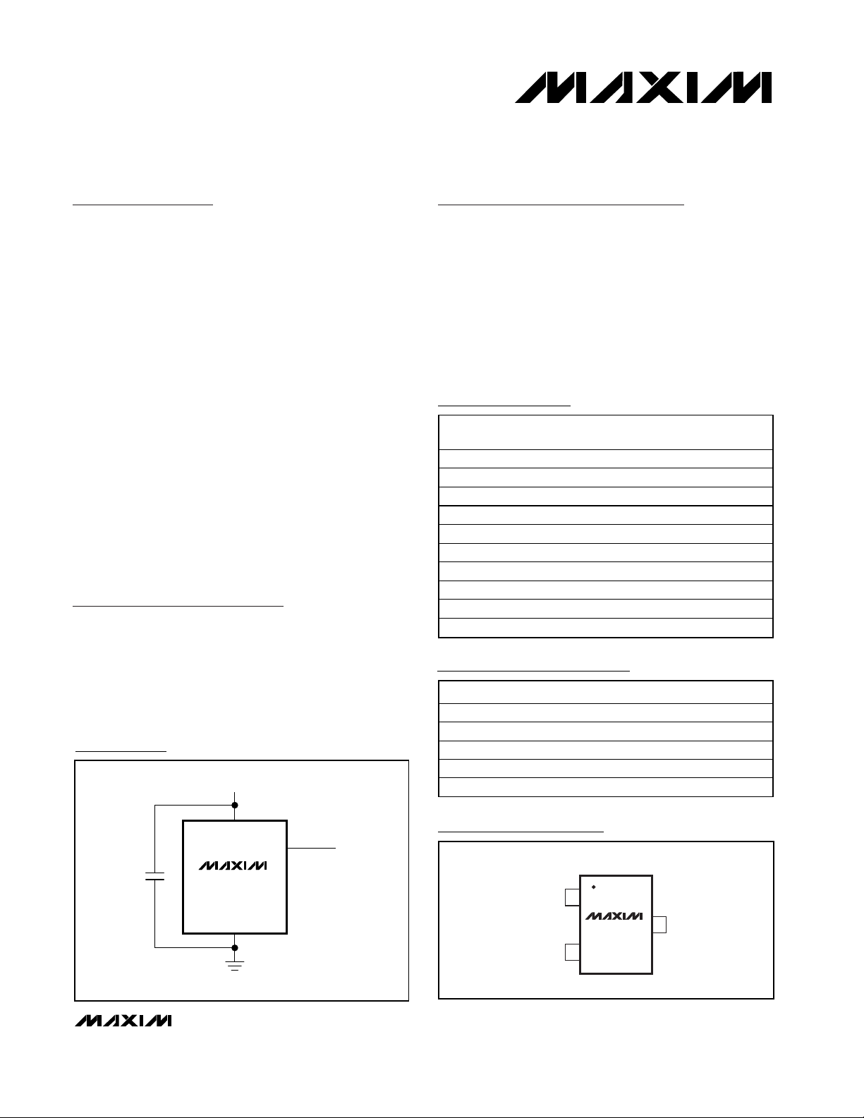
Typical Operating Circuit
+SUPPLY INPUT (SEE SELECTOR GUIDE)
PART TEMP RANGE
MAX6034AEXR21-T -40°C to +85°C 3 SC70-3 AJH
MAX6034BEXR21-T -40°C to +85°C 3 SC70-3 AJM
MAX6034AEXR25-T -40°C to +85°C 3 SC70-3 AJI
MAX6034BEXR25-T -40°C to +85°C 3 SC70-3 AJN
MAX6034AEXR30-T -40°C to +85°C 3 SC70-3 AJJ
MAX6034BEXR30-T -40°C to +85°C 3 SC70-3 AJO
MAX6034AEXR33-T -40°C to +85°C 3 SC70-3 AJK
MAX6034BEXR33-T -40°C to +85°C 3 SC70-3 AJP
MAX6034AEXR41-T -40°C to +85°C 3 SC70-3 AJL
MAX6034BEXR41-T -40°C to +85°C 3 SC70-3 AJQ
PART
MAX6034_EXR21-T 2.048 2.5 to 5.5
MAX6034_EXR25-T 2.500 (V
MAX6034_EXR30-T 3.000 (V
MAX6034_EXR33-T 3.300 (V
MAX6034_EXR41-T 4.096 (V
V
OUT INPUT VOLTAGE (V)
PI N PA C K A G E
+ 200mV) to 5.5
OUT
+ 200mV) to 5.5
OUT
+ 200mV) to 5.5
OUT
+ 200mV) to 5.5
OUT
MARK
TOP
IN
1
MAX6034
2
SC70
3 GND
*
*CAPACITOR IS OPTIONAL.
MAX6034
GND
OUT
REFERENCE
OUT
TOP VIEW
IN
OUT
MAX6034
Precision, Micropower, Low-Dropout, SC70
Series Voltage Reference
2 _______________________________________________________________________________________
ABSOLUTE MAXIMUM RATINGS
ELECTRICAL CHARACTERISTICS–MAX6034_21 (V
OUT
= 2.048V)
(VIN= 2.7V, I
OUT
= 0, TA= T
MIN
to T
MAX
, unless otherwise noted. Typical values are at TA= +25°C.) (Note 1)
Stresses beyond those listed under “Absolute Maximum Ratings” may cause permanent damage to the device. These are stress ratings only, and functional
operation of the device at these or any other conditions beyond those indicated in the operational sections of the specifications is not implied. Exposure to
absolute maximum rating conditions for extended periods may affect device reliability.
(Voltages Referenced to GND)
IN ...........................................................................-0.3V to +6.0V
OUT .............................................................-0.3V to (VIN+ 0.3V)
Output Short Circuit to GND or IN..............................Continuous
Continuous Power Dissipation (T
A
= +70°C)
3-Pin SC70 (derate 2.9mW/°C above +70°C).............235mW
Operating Temperature Range ...........................-40°C to +85°C
Junction Temperature......................................................+150°C
Storage Temperature Range .............................-65°C to +150°C
Lead Temperature (soldering, 10s) ................................+300°C
OUTPUT
Output Voltage V
Output Voltage Temperature
Coefficient (Note 2)
Line Regulation
Load Regulation
OUT Short-Circuit Current I
Temperature Hysteresis
Long-Term Stability
DYNAMIC
Noise Voltage e
Ripple Rejection
Turn-On Settling Time t
Capacitive-Load Stability Range C
INPUT
Supply Voltage Range V
Quiescent Supply Current I
Change in Supply Current Per
Change in Input Voltage
PARAMETER SYMBOL CONDITIONS MIN TYP MAX UNITS
OUT
TCV
∆V
OUT
∆V
∆V
OUT
∆I
OUT Sinking: 0 ≤ I
SC
∆V
OUT
cycle
∆V
OUT
time
OUT
∆V
OUT
∆V
OUT
IN
∆I
/∆VIN2.5V ≤ VIN ≤ 5.5V 4.1 16 µA/V
IN
TA = +25°C
MAX6034A_21 7 30
OUT
MAX6034B_21 7 75
/
2.5V ≤ VIN ≤ 5.5V 33 220 µV/V
IN
Sourcing: 0 ≤ I
/
Short to GND 12
Short to IN 4
/
(Note 3) 100 ppm
/
1000hr at T
f = 0.1Hz to 10Hz 45 µV
f = 10Hz to 10kHz 46 µV
/
VIN = 2.7V ±100mV, f = 120Hz 80 dB
IN
To V
R
C
OUT
(Note 4) 0 1 µF
Guaranteed by line-regulation test 2.5 5.5 V
IN
A
= 0.1% of final value,
OUT
= 50pF
MAX6034A_21 (±0.2%) 2.044 2.048 2.052
MAX6034B_21 (±0.4%) 2.040 2.048 2.056
≤ 1mA 0.25 1.0
OUT
≤ 200µA 2.1 62
OUT
= +25°C90
V
ppm/°C
mV/mA
mA
ppm/
1000hr
P-P
RMS
85 µs
85 115 µA
MAX6034
Precision, Micropower, Low-Dropout, SC70
Series Voltage Reference
_______________________________________________________________________________________ 3
ELECTRICAL CHARACTERISTICS–MAX6034_25 (V
OUT
= 2.500V)
(VIN= 2.7V, I
OUT
= 0, TA= T
MIN
to T
MAX
, unless otherwise noted. Typical values are at TA= +25°C.) (Note 1)
OUTPUT
Output Voltage V
Output Voltage Temperature
Coefficient (Note 2)
Line Regulation
Load Regulation
OUT Short-Circuit Current I
Dropout Voltage
Temperature Hysteresis
Long-Term Stability
DYNAMIC
Noise Voltage e
Ripple Rejection
Turn-On Settling Time t
Capacitive-Load Stability Range C
INPUT
Supply Voltage Range V
Quiescent Supply Current I
Change in Supply Current Per
Change in Input Voltage
PARAMETER SYMBOL CONDITIONS MIN TYP MAX UNITS
OUT
TCV
∆V
OUT
∆V
∆V
OUT
∆I
OUT Sinking: 0 ≤ I
SC
V
IN
V
OUT
∆V
OUT
cycle
∆V
OUT
time
OUT
∆V
OUT
∆V
OUT
IN
/∆VIN(V
∆I
IN
TA = +25°C
MAX6034A_25 7 30
OUT
MAX6034B_25 7 75
/
(V
IN
-
IN
R
IN
OUT
Sourcing: 0 ≤ I
/
Short to GND 12
Short to IN 4
I
OUT
/
(Note 3) 100 ppm
/
1000hr at T
f = 0.1Hz to 10Hz 55 µV
f = 10Hz to 10kHz 64 µV
/
VIN = 2.7V ±100mV, f = 120Hz 80 dB
To V
C
OUT
(Note 4) 0 1 µF
Guaranteed by line-regulation test
OUT
+ 200mV) ≤ VIN ≤ 5.5V 40 250 µV/V
= 1mA (Note 5) 70 200 mV
A
= 0.1% of final value,
OUT
= 50pF
+ 200mV) ≤ VIN ≤ 5.5V 4.2 16 µA/V
MAX6034A_25 (±0.2%) 2.495 2.500 2.505
MAX6034B_25 (±0.4%) 2.490 2.500 2.510
≤ 1mA 0.22 1.0
OUT
≤ 200µA 2.5 8
OUT
= +25°C90
V
OUT
+ 0.2
V
ppm/°C
mV/mA
mA
ppm/
1000hr
P-P
RMS
140 µs
5.5 V
85 115 µA
MAX6034
Precision, Micropower, Low-Dropout, SC70
Series Voltage Reference
4 _______________________________________________________________________________________
ELECTRICAL CHARACTERISTICS–MAX6034_30 (V
OUT
= 3.000V)
(VIN= 5V, I
OUT
= 0, TA= T
MIN
to T
MAX
, unless otherwise noted. Typical values are at TA= +25°C.) (Note 1)
OUTPUT
Output Voltage V
Output Voltage Temperature
Coefficient (Note 2)
Line Regulation
Load Regulation
OUT Short-Circuit Current I
Dropout Voltage V
Temperature Hysteresis
Long-Term Stability
DYNAMIC
Noise Voltage e
Ripple Rejection
Turn-On Settling Time t
Capacitive-Load Stability Range C
INPUT
Supply Voltage Range V
Quiescent Supply Current I
Change in Supply Current Per
Change in Input Voltage
PARAMETER SYMBOL CONDITIONS MIN TYP MAX UNITS
OUT
/
IN
/
TA = +25°C
MAX6034A_30
MAX6034B_30
(V
+ 200mV) ≤ VIN ≤ 5.5V
OUT
Sourcing: 0 ≤ I
Sinking: 0 ≤ I
OUT
OUT
≤ 200µA
TCV
∆V
∆V
∆V
∆I
OUT
OUT
OUT
OUT
Short to GND 13
SC
- V
IN
∆V
OUT
cycle
∆V
OUT
time
OUT
∆V
OUT
∆V
OUT
IN
∆I
/∆VIN(V
IN
Short to IN 4
I
OU T
/
/
= 1mA (Note 5)
OUT
(Note 3) 100 ppm
1000hr at T
= +25°C90
A
f = 0.1Hz to 10Hz
f = 10Hz to 10kHz
/
VIN = 5V ±100mV, f = 120Hz
IN
To V
R
C
= 0.1% of final value,
OUT
= 50pF
OUT
(Note 4)
Guaranteed by line-regulation test
IN
+ 200mV) ≤ V
OUT
MAX6034A_30 (±0.2%) 2.994 3.000 3.006
MAX6034B_30 (±0.4%) 2.988 3.000 3.012
730
775
43 280
≤ 1mA 0.30 1.3
2.6 8
70 200
66
80
76
165
01
V
OUT
+ 0.2
5.5
95 125
IN
≤ 5.5V
4.5 16
V
ppm/°C
µV/V
mV/mA
mA
mV
ppm/
1000hr
µV
P-P
µV
RMS
dB
µs
µF
V
µA
µA/V

MAX6034
Precision, Micropower, Low-Dropout, SC70
Series Voltage Reference
_______________________________________________________________________________________ 5
ELECTRICAL CHARACTERISTICS–MAX6034_33 (V
OUT
= 3.300V)
(VIN= 5V, I
OUT
= 0, TA= T
MIN
to T
MAX
, unless otherwise noted. Typical values are at TA= +25°C.) (Note 1)
OUTPUT
Output Voltage V
Output Voltage Temperature
Coefficient (Note 2)
Line Regulation
Load Regulation
OUT Short-Circuit Current I
Dropout Voltage V
Temperature Hysteresis
Long-Term Stability
DYNAMIC
Noise Voltage e
Ripple Rejection
Turn-On Settling Time t
Capacitive-Load Stability Range C
INPUT
Supply Voltage Range V
Quiescent Supply Current I
Change in Supply Current Per
Change in Input Voltage
PARAMETER SYMBOL CONDITIONS MIN TYP MAX UNITS
OUT
TCV
∆V
OUT
∆V
∆V
OUT
∆I
OUT Sinking: 0 ≤ I
SC
- V
IN
∆V
OUT
cycle
∆V
OUT
time
OUT
∆V
OUT
∆V
R
OUT
IN
IN
∆I
/∆VIN(V
IN
TA = +25°C
MAX6034A_33 7 30
OUT
MAX6034B_33 7 75
/
(V
Sourcing: 0 ≤ I
/
OUT
IN
Short to GND 13
Short to IN 4
I
OU T
OUT
/
(Note 3) 100 ppm
/
1000hr at T
f = 0.1Hz to 10Hz 73 µV
f = 10Hz to 10kHz 88 µV
/
VIN = 5V ±100mV, f = 120Hz 76 dB
IN
To V
C
OUT
(Note 4) 0 1 µF
Guaranteed by line-regulation test
OUT
+ 200mV) ≤ VIN ≤ 5.5V 45 300 µV/V
= 1mA (Note 5) 70 200 mV
= 0.1% of final value,
OUT
= 50pF
+ 200mV) ≤ V
MAX6034A_33 (±0.2%) 3.293 3.300 3.307
MAX6034B_33 (±0.4%) 3.287 3.300 3.313
≤ 1mA 0.3 1.3
OUT
≤ 200µA 3 8.6
OUT
= +25°C90
A
≤ 5.5V 3.8 16 µA/V
IN
V
OUT
+ 0.2
V
ppm/°C
mV/mA
mA
ppm/
1000hr
P-P
RMS
200 µs
5.5 V
95 125 µA

MAX6034
Precision, Micropower, Low-Dropout, SC70
Series Voltage Reference
6 _______________________________________________________________________________________
ELECTRICAL CHARACTERISTICS–MAX6034_41 (V
OUT
= 4.096V)
(VIN= 5V, I
OUT
= 0, TA= T
MIN
to T
MAX
, unless otherwise noted. Typical values are at TA= +25°C.) (Note 1)
Note 1: All devices are 100% production tested at TA= +25°C and are guaranteed by design for TA= T
MIN
to T
MAX
as specified.
Note 2: Temperature coefficient is measured by the “box” method, i.e. the maximum ∆V
OUT
/ V
OUT
is divided by the maximum ∆T.
Note 3: Temperature hysteresis is defined as the change in +25°C output voltage after cycling the device from T
MIN
to T
MAX
.
Note 4: Not production tested. Guaranteed by design.
Note 5: Dropout voltage is defined as the minimum differential voltage (V
IN
- V
OUT)
at which V
OUT
decreases by 0.2% from its
original value at V
IN
= 5.0V (VIN= 2.7V for MAX6034_25).
OUTPUT
Output Voltage V
Output Voltage Temperature
Coefficient (Note 2)
Line Regulation
Load Regulation
OUT Short-Circuit Current I
Dropout Voltage V
Temperature Hysteresis
Long-Term Stability
DYNAMIC
Noise Voltage e
Ripple Rejection
Turn-On Settling Time t
Capacitive-Load Stability Range C
INPUT
Supply Voltage Range V
Quiescent Supply Current I
Change in Supply Current Per
Change in Input Voltage
PARAMETER SYMBOL CONDITIONS MIN TYP MAX UNITS
OUT
/
IN
/
TA = +25°C
MAX6034A_41
MAX6034B_41
(V
+ 200mV) ≤ VIN ≤ 5.5V
OUT
Sourcing: 0 ≤ I
Sinking: 0 ≤ I
OUT
OUT
TCV
∆V
∆V
∆V
∆I
OUT
OUT
OUT
OUT
Short to GND 13
SC
- V
IN
∆V
OUT
cycle
∆V
OUT
time
OUT
∆V
OUT
∆V
OUT
IN
/∆VIN(V
∆I
IN
Short to IN 7
OU TIOUT
/
/
= 1mA (Note 5)
(Note 3) 100 ppm
1000hr at T
= +25°C90
A
f = 0.1Hz to 10Hz
f = 10Hz to 10kHz
/
VIN = 5V ±100mV, f = 120Hz
IN
To V
R
C
= 0.1% of final value,
OUT
= 50pF
OUT
(Note 4)
Guaranteed by line-regulation test
IN
+ 200mV) ≤ V
OUT
MAX6034A_41 (±0.2%) 4.088 4.096 4.104
MAX6034B_41 (±0.4%) 4.080 4.096 4.112
730
775
50 350
≤ 1mA 0.35 1.5
≤ 200µA
3.4 9.8
70 200
90
105
73
260
01
V
OUT
+ 0.2
5.5
95 125
IN
≤ 5.5V
4.7 16
V
ppm/°C
µV/V
mV/mA
mA
mV
ppm/
1000hr
µV
P-P
µV
RMS
dB
µs
µF
V
µA
µA/V

MAX6034
Precision, Micropower, Low-Dropout, SC70
Series Voltage Reference
_______________________________________________________________________________________ 7
Typical Operating Characteristics
(VIN= 2.7V for MAX6034_21/25, VIN= 5V for MAX6034_30/33/41, I
OUT
= 0, TA= +25°C, unless otherwise noted.) (Note 6)
OUTPUT VOLTAGE TEMPERATURE DRIFT
2.053
THREE TYPICAL PARTS
2.051
2.049
2.047
OUTPUT VOLTAGE (V)
2.045
2.043
-40 85
MAX6034_21
= 2.048V)
(V
OUT
TEMPERATURE (°C)
OUTPUT VOLTAGE TEMPERATURE DRIFT
4.106
THREE TYPICAL PARTS
MAX6034 toc01
4.102
4.098
4.094
OUTPUT VOLTAGE (V)
4.090
4.086
603510-15
-40 85
MAX6034_41
SUPPLY CURRENT
vs. SUPPLY VOLTAGE
4.098
4.097
LONG-TERM DRIFT
= 4.096V)
(V
OUT
MAX6034 toc04
105
100
MAX6034_41
= 4.096V)
(V
OUT
603510-15
TEMPERATURE (°C)
2.050
MAX6034 toc02
2.049
2.048
OUTPUT VOLTAGE (V)
2.047
2.046
MAX6034 toc05
0400200 600 800 1000
SUPPLY CURRENT vs. TEMPERATURE
110
105
100
MAX6034_21
LONG-TERM DRIFT
(V
OUT
TIME (hr)
VIN = 5.5V
= 2.048V)
MAX6034 toc03
MAX6034 toc06
4.096
OUTPUT VOLTAGE (V)
4.095
4.094
0 400200 600 800 1000
TIME (hr)
95
SUPPLY CURRENT (µA)
90
85
2.5 5.5
MAX6034_25
DROPOUT VOLTAGE vs. SOURCE CURRENT
= 2.500V)
(V
0.6
0.5
0.4
0.3
0.2
DROPOUT VOLTAGE (V)
0.1
0
05
OUT
TA = +85°C
TA = +25°C
SOURCE CURRENT (mA)
MAX6034 toc07
TA = -40°C
4321
DROPOUT VOLTAGE vs. SINK CURRENT
0.15
0.10
0.05
DROPOUT VOLTAGE (V)
0
01.0
SUPPLY VOLTAGE (V)
MAX6034_25
= 2.500V)
(V
OUT
TA = +85°C
TA = +25°C
TA = -40°C
SINK CURRENT (mA)
95
90
SUPPLY CURRENT (µA)
85
80
5.04.54.03.53.0
-40 85
VIN = 2.7V
603510-15
TEMPERATURE (°C)
MAX6034_41
DROPOUT VOLTAGE vs. SOURCE CURRENT
= 4.096V)
(V
0.6
0.5
MAX6034 toc08
0.4
0.3
0.2
DROPOUT VOLTAGE (V)
0.1
0
0.80.60.40.2
05
OUT
TA = +85°C
TA = +25°C
SOURCE CURRENT (mA)
MAX6034 toc09
TA = -40°C
4321

MAX6034
Precision, Micropower, Low-Dropout, SC70
Series Voltage Reference
8 _______________________________________________________________________________________
Typical Operating Characteristics (continued)
(VIN= 2.7V for MAX6034_21/25, VIN= 5V for MAX6034_30/33/41, I
OUT
= 0, TA= +25°C, unless otherwise noted.) (Note 6)
V
OUT
100mV/div
AC-COUPLED
V
IN
5.5V
5.0V
100µs
MAX6034_41
LINE TRANSIENT
(V
OUT
= 4.096V)
MAX6034 toc17
C
LOAD
= 0
V
OUT
50mV/div
AC-COUPLED
V
IN
2.95V
2.70V
100µs
MAX6034_25
LINE TRANSIENT
(V
OUT
= 2.500V)
MAX6034 toc16
C
LOAD
= 0
MAX6034 toc15
FREQUENCY (kHz)
PSRR (dB)
1001010.10.01
-80
-60
-40
-20
0
-100
0.001 1000
MAX6034_41
POWER-SUPPLY REJECTION RATIO
vs. FREQUENCY (V
OUT
= 4.096V)
MAX6034 toc14
FREQUENCY (kHz)
PSRR (dB)
1001010.10.01
-80
-60
-40
-20
0
-100
0.001 1000
MAX6034_25
POWER-SUPPLY REJECTION RATIO
vs. FREQUENCY (V
OUT
= 2.500V)
MAX6034 toc13
INPUT VOLTAGE (V)
OUTPUT VOLTAGE CHANGE (µV)
5.04.54.03.53.0
-80
-60
-40
-20
0
20
-100
2.5 5.5
MAX6034_25
LINE REGULATION
(V
OUT
= 2.500V)
TA = +85°C
TA = -40°C
TA = +25°C
MAX6034 toc12
LOAD CURRENT (mA)
OUTPUT VOLTAGE CHANGE (mV)
43210
-2
-1
0
1
2
3
-3
-1 5
MAX6034_41
LOAD REGULATION
(V
OUT
= 4.096V)
TA = +85°C
TA = +85°C
TA = +25°C
TA = -40°C
TA = -40°C
TA = +25°C
SINK
SOURCE
MAX6034 toc11
LOAD CURRENT (mA)
OUTPUT VOLTAGE CHANGE (mV)
43210
-2
-1
0
1
2
3
-3
-1 5
MAX6034_21
LOAD REGULATION
(V
OUT
= 2.048V)
TA = +25°C
TA = +85°C
TA = +25°C
SINK
SOURCE
TA = -40°C
TA = -40°C
TA = +85°C
MAX6034 toc10
SINK CURRENT (mA)
DROPOUT VOLTAGE (V)
0.80.60.40.2
0.05
0.10
0.15
0
01.0
MAX6034_41
DROPOUT VOLTAGE vs. SINK CURRENT
(V
OUT
= 4.096V)
TA = +85°C
TA = +25°C
TA = -40°C

MAX6034
Precision, Micropower, Low-Dropout, SC70
Series Voltage Reference
_______________________________________________________________________________________ 9
Typical Operating Characteristics (continued)
(VIN= 2.7V for MAX6034_21/25, VIN= 5V for MAX6034_30/33/41, I
OUT
= 0, TA= +25°C, unless otherwise noted.) (Note 6)
V
OUT
10mV/div
AC-COUPLED
I
OUT
+10µA
-10µA
1ms
MAX6034_25
LOAD TRANSIENT
C
LOAD
= 0
I
LOAD
= ±10µA
V
OUT
= 2.5V
MAX6034 toc18
V
OUT
2mV/div
AC-COUPLED
I
OUT
+10µA
-10µA
1ms
MAX6034_25
LOAD TRANSIENT
C
LOAD
= 1µF
I
LOAD
= ±10µA
V
OUT
= 2.5V
MAX6034 toc19
V
OUT
2mV/div
AC-COUPLED
I
OUT
+10µA
-10µA
1ms
MAX6034_41
LOAD TRANSIENT
C
LOAD
= 1µF
I
LOAD
= ±10µA
V
OUT
= 4.096V
MAX6034 toc21
V
OUT
10mV/div
AC-COUPLED
I
OUT
+10µA
-10µA
1ms
MAX6034_41
LOAD TRANSIENT
MAX6034 toc20
C
LOAD
= 0
I
LOAD
= ±10µA
V
OUT
= 4.096V
V
OUT
20mV/div
AC-COUPLED
I
OUT
+1mA
-0.2mA
1ms
MAX6034_25
LOAD TRANSIENT
MAX6034 toc23
C
LOAD
= 1µF
I
LOAD
= +1mA/-0.2mA
V
OUT
= 2.5V
V
OUT
100mV/div
AC-COUPLED
I
OUT
+1mA
-0.2mA
1ms
MAX6034_25
LOAD TRANSIENT
C
LOAD
= 0
I
LOAD
= +1mA/-0.2mA
V
OUT
= 2.5V
MAX6034 toc22

MAX6034
Precision, Micropower, Low-Dropout, SC70
Series Voltage Reference
10 ______________________________________________________________________________________
Typical Operating Characteristics (continued)
(VIN= 2.7V for MAX6034_21/25, VIN= 5V for MAX6034_30/33/41, I
OUT
= 0, TA= +25°C, unless otherwise noted.) (Note 6)
Note 6: Many of the MAX6034 family Typical Operating Characteristics are extremely similar. The extremes of these characteristics are
found in the MAX6034_21 (2.048V output) and the MAX6034_41 (4.096V output). The Typical Operating Characteristics of the
remainder of the MAX6034 family typically lie between those two extremes and can be estimated based on their output voltages.
1s
MAX6034_41
OUTPUT NOISE (0.1Hz TO 10Hz)
MAX6034 toc29
V
OUT
= 4.096V
50µV/div
1s
MAX6034_25
OUTPUT NOISE (0.1Hz TO 10Hz)
MAX6034 toc28
V
OUT
= 2.5V
50µV/div
40µs
MAX6034_41
TURN-ON TRANSIENT
MAX6034 toc27
C
LOAD
= 50pF
V
OUT
= 4.096V
V
IN
5V
0
V
OUT
4.096V
0
V
IN
2.7V
0
V
OUT
2.5V
0
40µs
MAX6034_25
TURN-ON TRANSIENT
MAX6034 toc26
C
LOAD
= 50pF
V
OUT
= 2.5V
V
OUT
50mV/div
AC-COUPLED
I
OUT
+1mA
-0.2mA
1ms
MAX6034_41
LOAD TRANSIENT
MAX6034 toc25
C
LOAD
= 1µF
I
LOAD
= +1mA/-0.2mA
V
OUT
= 4.096V
V
OUT
100mV/div
AC-COUPLED
I
OUT
+1mA
-0.2mA
1ms
MAX6034_41
LOAD TRANSIENT
MAX6034 toc24
C
LOAD
= 0
I
LOAD
= +1mA/-0.2mA
V
OUT
= 4.096V

MAX6034
Precision, Micropower, Low-Dropout, SC70
Series Voltage Reference
______________________________________________________________________________________ 11
Detailed Description
The MAX6034 family of precision bandgap references
use a proprietary temperature coefficient curvature-correction circuit and laser-trimmed, thin-film resistors,
resulting in a low temperature coefficient of less than
30ppm/°C and initial accuracy of better than 0.2%.
These devices can source up to 1mA and sink up to
200µA with less than 200mV of dropout voltage, making
them attractive for use in low-voltage applications.
Applications Information
Input Bypassing
For the best line-transient performance, decouple the
input with a 0.1µF ceramic capacitor as shown in the
Typical Operating Circuit. Locate the capacitor as
close to IN as possible.
Output/Load Capacitance
Devices in the MAX6034 family do not require an output
capacitor for frequency stability. They are stable for
capacitive loads from 0 to 1µF. However, in applications where the load or the supply can experience step
changes, an output capacitor reduces the amount of
overshoot (or undershoot) and improves the circuit’s
transient response. Many applications do not need an
external capacitor, and the MAX6034 can offer a significant advantage in these applications when board
space is critical.
Supply Current
The quiescent supply current of the series-mode
MAX6034 family is typically 90µA and is virtually independent of the supply voltage, with only a 16µA/V
(max) variation with supply voltage.
When the supply voltage is below the minimum-specified input voltage (as during turn-on), the device can
draw up to 50µA beyond the nominal supply current.
The input-voltage source must be capable of providing
this current to ensure reliable turn-on.
Output Voltage Hysteresis
Output voltage hysteresis is the change in the output
voltage at TA= +25°C before and after the device is
cycled over its entire operating temperature range.
Hysteresis is caused by differential package stress
appearing across the bandgap core transistors. The
typical temperature hysteresis value for the MAX6034
family is 100ppm.
Turn-On Time
These devices typically turn on and settle to within
0.1% of their final value in 85µs to 260µs depending on
the device. The turn-on time can increase up to 1.25ms
with the device operating at the minimum dropout voltage and the maximum load.
Temperature Coefficient vs.
Operating Temperature Range for a 1LSB
Maximum Error
In a data converter application, the reference voltage of
the converter must stay within a certain limit to keep the
error in the data converter smaller than the resolution
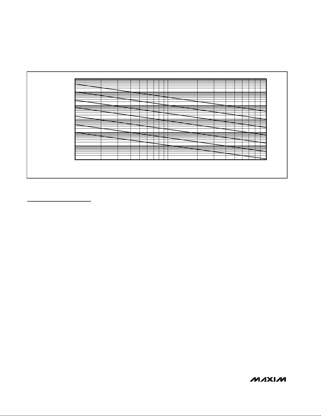
limit through the operating temperature range. Figure 1
shows the maximum allowable reference voltage temperature coefficient to keep the conversion error to less
than 1LSB, as a function of the operating temperature
range (T
MAX
- T
MIN
) with the converter resolution as a
parameter. The graph assumes the reference-voltage
temperature coefficient as the only parameter affecting
accuracy.
In reality, the absolute static accuracy of a data converter is dependent on the combination of many parameters such as integral nonlinearity, differential
nonlinearity, offset error, gain error, as well as voltage
reference changes.
Pin Description
PIN NAME FUNCTION
1 IN Supply Voltage Input
2 OUT Reference Voltage Output
3 GND Ground
MAX6034
Precision, Micropower, Low-Dropout, SC70
Series Voltage Reference
12 ______________________________________________________________________________________
Chip Information
TRANSISTOR COUNT: 113
PROCESS: BiCMOS
Figure 1. Temperature Coefficient vs. Operating Temperature Range for a 1LSB Maximum Error
10,000
1000
100
TEMPERATURE
COEFFICIENT
(ppm/°C)
10
1
0.1
0.01
110
OPERATING TEMPERATURE RANGE (T
MAX
- T
MIN
) (°C)
8 BIT
10 BIT
12 BIT
14 BIT
16 BIT
18 BIT
20 BIT
100
MAX6034
Precision, Micropower, Low-Dropout, SC70
Series Voltage Reference
Maxim cannot assume responsibility for use of any circuitry other than circuitry entirely embodied in a Maxim product. No circuit patent licenses are
implied. Maxim reserves the right to change the circuitry and specifications without notice at any time.
Maxim Integrated Products, 120 San Gabriel Drive, Sunnyvale, CA 94086 408-737-7600 ____________________ 13
© 2002 Maxim Integrated Products Printed USA is a registered trademark of Maxim Integrated Products.
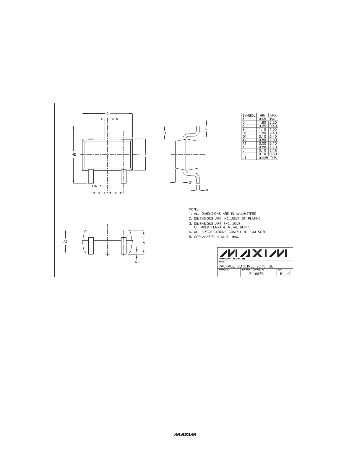
Package Information
SC70, 3L.EPS
 Loading...