

Page 1
General Description
The MAX6033 ultra-high-precision series voltage reference features a low 7ppm/°C (max) temperature coefficient and a low dropout voltage (200mV, max). Low
temperature drift and low noise make the MAX6033
ideal for use with high-resolution ADCs or DACs.
This device uses bandgap technology for low-noise performance and excellent accuracy. Laser-trimmed, highstability, thin-film resistors, and postpackage trimming
guarantee excellent initial accuracy (±0.04%, max). The
MAX6033 consumes only 40µA of supply current and
sources up to 15mA. Series mode references save system power and use minimal external components compared to two-terminal shunt references.
The MAX6033 is available in the miniature 6-pin SOT23
package and is offered over the automotive temperature range (-40°C to +125°C).
Applications
Precision Regulators
A/D and D/A Converters
Power Supplies
Hard-Disk Drives
High-Accuracy Industrial and Process Control
Hand-Held Instruments
Features
o Tiny 6-Pin SOT23 Package
o Ultra-Low Temperature Drift: 7ppm/°C (max)
o ±0.04% Initial Accuracy
o Stable with Capacitive Loads
o Low 16µV
P-P
Noise (0.1Hz to 10Hz) (2.5V Output)
o 15mA Output Source Current
o Low 200mV Dropout Voltage
o Low 40µA Quiescent Current
o Wide 2.7V to 12.6V Supply Voltage
o Excellent Load Regulation: 0.001mV/mA
MAX6033
Ultra-High-Precision SOT23 Series
Voltage Reference
________________________________________________________________
Maxim Integrated Products
1
Ordering Information/Selector Guide
19-2300; Rev 3; 3/12
For pricing, delivery, and ordering information, please contact Maxim Direct at 1-888-629-4642,
or visit Maxim’s website at www.maxim-ic.com.
Ordering Information/Selector Guide continued on last page.
#
Denotes a RoHS-compliant device that may include lead(Pb) that is exempt under the RoHS requirements.
T = Tape and reel.
Typical Operating Circuit appears at end of data sheet.
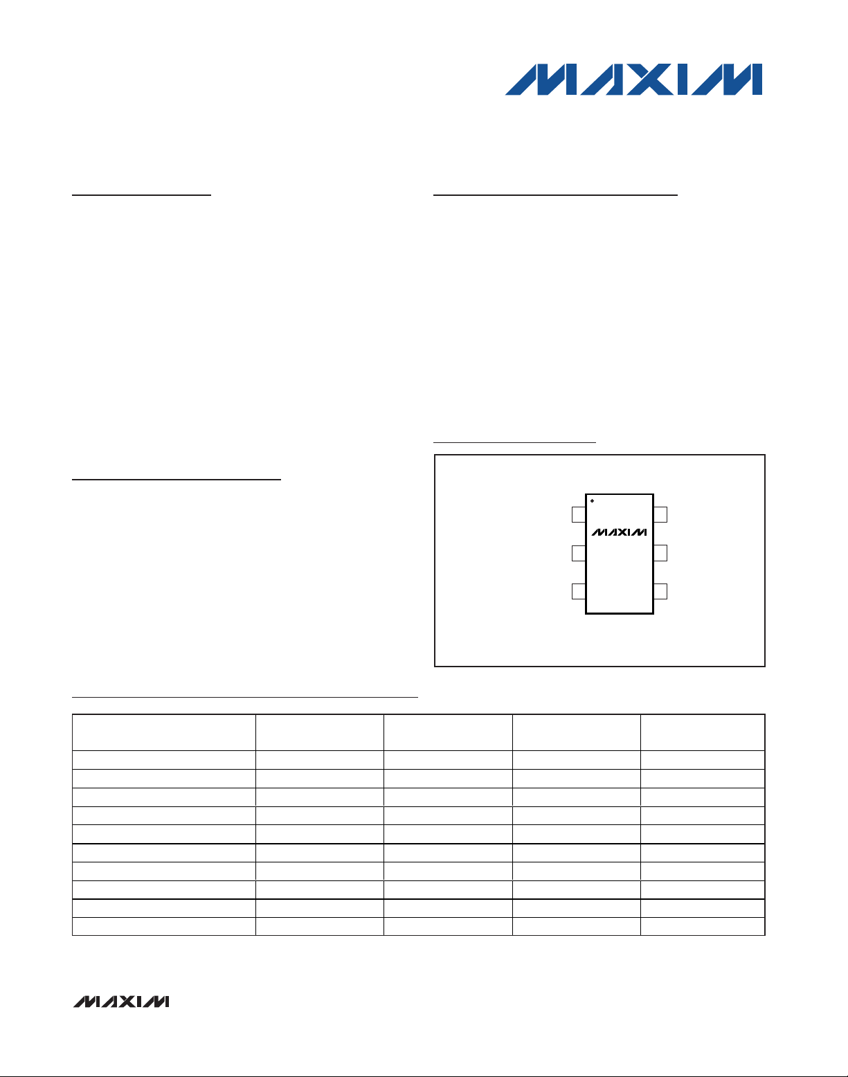
GND
INI.C.*
*I.C. = INTERNALLY CONNECTED: DO NOT USE
16OUTS
5 OUTF
I.C.*
SOT23
TOP VIEW
2
34
MAX6033
Pin Configuration
PART
MAX6033AAUT25-T 2.500 10 0.04 ABDF
MAX6033AAUT25#TG16 2.500 10 0.04 #ACNC
MAX6033BAUT25-T 2.500 15 0.20 AAXL
MAX6033BAUT25#TG16 2.500 15 0.20 #ACND
MAX6033CAUT25-T 2.500 40 0.10 AAXH
MAX6033CAUT25#TG16 2.500 40 0.10 #ACNE
MAX6033AAUT30-T 3.300 10 0.04 ABDG
MAX6033AAUT30#TG16 3.300 10 0.04 #ACNF
MAX6033BAUT30-T 3.300 15 0.20 AAXM
MAX6033BAUT30#TG16 3.300 15 0.20 #ACNG
OUTPUT
VOLTAGE (V)
TEMP COEFF
(ppm/°C)
INITIAL ACCURACY
(%)
TOP MARK
Page 2
MAX6033
Ultra-High-Precision SOT23 Series
Voltage Reference
2 _______________________________________________________________________________________
ABSOLUTE MAXIMUM RATINGS
ELECTRICAL CHARACTERISTICS—V
OUT
= 2.500V
(VIN= 5V, C
OUT
= 0.1µF, I
OUT
= 0A, TA= T
MIN
to T
MAX
, unless otherwise specified. Typical values are at TA= +25°C.) (Note 1)
Stresses beyond those listed under “Absolute Maximum Ratings” may cause permanent damage to the device. These are stress ratings only, and functional
operation of the device at these or any other conditions beyond those indicated in the operational sections of the specifications is not implied. Exposure to
absolute maximum rating conditions for extended periods may affect device reliability.
IN to GND ...............................................................-0.3V to +13V
OUTF, OUTS to GND................................................-0.3V to +6V
Continuous Power Dissipation (TA= +70°C)
6-Pin SOT23 (derate 9.1mW/°C above +70°C)............727mW
Operating Temperature Range .........................-40°C to +125°C
Storage Temperature Range .............................-65°C to +150°C
Maximum Junction Temperature .....................................+150°C
Lead Temperature (soldering, 10s) .................................+300°C
Soldering Temperature (reflow)
RoHS-Compliant Packages ..........................................+245°C
Packages Containing Lead(Pb)....................................+240°C
Output Voltage V
Output-Voltage Accuracy TA = +25°C
Output Voltage Temperature
Coefficient
Input Voltage Range V
Line Regulation
Load Regulation
Dropout Voltage (Note 2) V
Quiescent Supply Current I
Output Short-Circuit Current I
Output-Voltage Noise e
Turn-On Settling Time t
Temperature Hysteresis (Note 3)
Long-Term Stability ∆t = 1000hr
PARAMETER SYMBOL CONDITIONS MIN TYP MAX UNITS
TCV
∆V
∆V
∆V
∆I
OUT
OUT
IN
OUT
OUT
OUT
DO
IN
SC
n
ON
/
IN
/
TA = +25°C
MAX6033A
MAX6033B
MAX6033C
Inferred from line regulation specification
2.7V ≤ VIN ≤ 12.6V
-100µA ≤ I
15mA
V
= 0.1%, I
OUT
V
= 0.1%,
OUT
= 10mA
I
OUT
TA = +25oC
TA = -40oC to +85oC
TA = -40oC to +125oC
V
= 0V
OUT
V
= V
OUT
0.1Hz ≤ f ≤ 10Hz
10Hz ≤ f ≤ 1kHz
V
settles to ±0.01% of final value
OUT
OUT
IN
≤
= 1mA
OUT
MAX6033A
MAX6033B
MAX6033C
MAX6033A
MAX6033B
MAX6033C
TA = -40oC to +85oC
= -40oC to +125oC
T
A
TA = -40oC to +85oC
= -40oC to +125oC
T
A
TA = -40oC to +85oC
= -40oC to +125oC
T
A
TA = +25°C
= -40°C to +125°C
T
A
TA = +25°C
= -40°C to +125°C
T
A
TA = -40oC to +85oC
T
= - 40oC to + 125oC
A
2.4990 2.5000 2.5010
2.4950 2.5000 2.5050
2.4975 2.5000 2.5025
-0.04 +0.04
-0.2 +0.2
-0.1 +0.1
1.5 7
2.5 10
310
715
620
10 40
2.7 12.6
325
50
0.001 0.05
0.1
0.02 0.2
0.3 0.4
0.5
40 60
75
85
90
-2
16
12
500
150
40
V
%
ppm/°C
V
µV/V
mV/mA
V
µA
mA
µV
P-P
µV
RMS
µs
ppm
ppm
Page 3
MAX6033
Ultra-High-Precision SOT23 Series
Voltage Reference
_______________________________________________________________________________________ 3
ELECTRICAL CHARACTERISTICS—V
OUT
= 3.000V
(VIN= 5V, C
OUT
= 0.1µF, I
OUT
= 0A, TA= T
MIN
to T
MAX
, unless otherwise specified. Typical values are at TA= +25°C.) (Note 1)
ELECTRICAL CHARACTERISTICS—V
OUT
= 4.096V
(VIN= 5V, C
OUT
= 0.1µF, I
OUT
= 0A, TA= T
MIN
to T
MAX
, unless otherwise specified. Typical values are at TA= +25°C.) (Note 1)
Output Voltage V
Output-Voltage Temperature
Coefficient
Input Voltage Range V
Line Regulation
Load Regulation
Dropout Voltage (Note 2) V
Quiescent Supply Current I
Output Short-Circuit Current I
Output-Voltage Noise e
Turn-On Settling Time t
Temperature Hysteresis (Note 3) 150 ppm
Long-Term Stability ∆t = 1000hr 40 ppm
PARAMETER SYMBOL CONDITIONS MIN TYP MAX UNITS
TCV
∆V
∆V
∆V
∆I
OUT
OUT
IN
OUT
IN
OUT
OUT
DO
IN
SC
n
ON
/
/
TA = +25oC
MAX6033A
MAX6033B
MAX6033C
Inferred from line regulation specification 3.2 12.6 V
3.2V ≤ VIN ≤ 12.6V
-100µA ≤ I
15mA
∆V
OUT
TA = +25°C4060
TA = -40°C to +85°C75
TA = -40°C to +125°C 85
V
= 0V 90
OUT
V
= V
OUT
0.1Hz ≤ f ≤ 10Hz 24 µV
10Hz ≤ f ≤ 1kHz 15 µV
V
settles to ±0.01% of final value 600 µs
OUT
OUT
= 0.1%
IN
MAX6033A 2.9988 3.0000 3.0012
MAX6033B 2.9940 3.0000 3.0060
MAX6033C 2.9970 3.0000 3.0030
MAX6033A -0.04 +0.04
MAX6033B -0.2 +0.2Output-Voltage Accuracy TA = +25oC
MAX6033C -0.1 +0.1
TA = -40oC to +85oC 1.5 7
T
TA = -40oC to +85oC310
T
TA = -40oC to +85oC620
T
TA = +25°C 4 30
T
≤
TA = +25°C 0.002 0.06
T
I
I
= -40oC to +125oC 2.5 10
A
= -40oC to +125oC715
A
= -40oC to +125oC1040
A
= -40°C to +125°C 60
A
= -40°C to +125°C 0.12
A
= 1mA 0.02 0.2
OUT
= 10mA 0.2 0.4
OUT
-2
V
%
ppm/°C
µV/V
mV/mA
V
µA
mA
P-P
RMS
Output Voltage V
PARAMETER SYMBOL CONDITIONS MIN TYP MAX UNITS
OUT
TA = +25°C
MAX6033A 4.0943 4.0960 4.0977
MAX6033B 4.0878 4.0960 4.1042
MAX6033C 4.0919 4.0960 4.1001
MAX6033A -0.04 +0.04
MAX6033B -0.2 +0.2Output-Voltage Accuracy TA = +25°C
MAX6033C -0.1 +0.1
V
%
Page 4
MAX6033
Ultra-High-Precision SOT23 Series
Voltage Reference
4 _______________________________________________________________________________________
ELECTRICAL CHARACTERISTICS—V
OUT
= 4.096V (continued)
(VIN= 5V, C
OUT
= 0.1µF, I
OUT
= 0A, TA= T
MIN
to T
MAX
, unless otherwise specified. Typical values are at TA= +25°C.) (Note 1)
ELECTRICAL CHARACTERISTICS—V
OUT
= 5.000V
(VIN= 5.5V, C
OUT
= 0.1µF, I
OUT
= 0A, TA= T
MIN
to T
MAX
, unless otherwise specified. Typical values are at TA= +25°C.) (Note 1)
Output-Voltage Temperature
Coefficient
PARAMETER SYMBOL CONDITIONS MIN TYP MAX UNITS
TCV
OUT
MAX6033A
MAX6033B
MAX6033C
Input-Voltage Range V
∆V
∆V
∆I
OUT
∆V
OUT
OUT
DO
IN
SC
ON
Line Regulation
Load Regulation
Dropout Voltage (Note 2) V
Output Short-Circuit Current I
Output-Voltage Noise e
Turn-On Settling Time t
Temperature Hysteresis (Note 3) 150 ppm
Long-Term Stability ∆t = 1000hr 40 ppm
Inferred from line regulation specification 4.3 12.6 V
IN
/
4.3V ≤ VIN ≤ 12.6V
IN
/
-100µA ≤ I
15mA
∆V
OUT
TA = +25°C 40 60
TA = -40°C to +85°C 75Quiescent Supply Current I
TA = -40oC to +125oC
V
= 0V 90
OUT
V
= V
OUT
0.1Hz ≤ f ≤ 10Hz 32 µV
n
10Hz ≤ f ≤ 1kHz 22 µV
V
settles to ±0.01% of final value 800 µs
OUT
TA = -40oC to +85oC 1.5 7
= -40oC to +125oC 2.5 10
T
A
TA = -40oC to +85oC310
T
= -40oC to +125oC715
A
TA = -40oC to +85oC620
T
= -40oC to +125oC1040
A
TA = +25°C 6 30
= -40oC to +125oC60
T
A
OUT
= 0.1%
IN
≤
TA = +25°C 0.002 0.08
T
= -40oC to +125oC 0.15
A
I
OUT
I
OUT
= 1mA 0.02 0.2
= 10mA 0.2 0.4
-2
ppm/°C
µV/V
mV/mA
V
µA
85
mA
P-P
RMS
Output Voltage V
Output-Voltage Temperature
Coefficient
Input Voltage Range V
PARAMETER SYMBOL CONDITIONS MIN TYP MAX UNITS
TCV
OUT
OUT
IN
TA = +25°C
MAX6033A
MAX6033B
MAX6033C
Inferred from line regulation specification 5.2 12.6 V
MAX6033A 4.9980 5.000 5.0020
MAX6033B 4.9900 5.000 5.0100
MAX6033C 4.9950 5.000 5.0050
MAX6033A -0.04 +0.04
MAX6033B -0.2 +0.2Output-Voltage Accuracy TA = +25°C
MAX6033C -0.1 +0.1
TA = -40oC to +85oC 1.5 7
= -40oC to +125oC 2.5 10
T
A
TA = -40oC to +85oC310
= -40oC to +125oC715
T
A
TA = -40oC to +85oC620
T
= -40oC to +125oC1040
A
V
%
ppm/°C
Page 5

MAX6033
Ultra-High-Precision SOT23 Series
Voltage Reference
_______________________________________________________________________________________ 5
ELECTRICAL CHARACTERISTICS—V
OUT
= 5.000V (continued)
(VIN= 5.5V, C
OUT
= 0.1µF, I
OUT
= 0A, TA= T
MIN
to T
MAX
, unless otherwise specified. Typical values are at TA= +25°C.) (Note 1)
Typical Operating Characteristics
(VIN= 5V, C
OUT
= 0.1µF, I
OUT
= 0A, TA= +25°C, unless otherwise specified.) (Note 4)
Note 1: MAX6033 is 100% production tested at T
A
= +25°C and is guaranteed by design for TA= T
MIN
to T
MAX
as specified.
Note 2: Dropout Voltage is the minimum input voltage at which V
OUT
changes ≤ 0.1% from V
OUT
at VIN= 5V (VIN= 5.5V for
V
OUT
= 5V).
Note 3: Temperature Hysteresis is defined as the change in +25°C output voltage before and after cycling the device
from T
MAX
to T
MIN
.
OUTPUT VOLTAGE vs.
TEMPERATURE (V
OUT
= 2.5V)
MAX6033 toc01
TEMPERATURE (°C)
OUTPUT VOLTAGE (V)
1109565 80-10 5 20 35 50-25
2.4982
2.4984
2.4986
2.4988
2.4990
2.4992
2.4994
2.4996
2.4998
2.5000
2.5002
2.5004
2.5006
2.5008
2.5010
2.4980
-40 125
3 TYPICAL UNITS
OUTPUT VOLTAGE vs.
TEMPERATURE (V
OUT
= 5V)
MAX6033 toc02
TEMPERATURE (°C)
OUTPUT VOLTAGE (V)
1109565 80-10 5 20 35 50-25
4.9982
4.9984
4.9986
4.9988
4.9990
4.9992
4.9994
4.9996
4.9998
5.0000
5.0002
5.0004
5.0006
5.0008
5.0010
4.9980
-40 125
3 TYPICAL UNITS
LOAD REGULATION
(V
OUT
= 2.5V)
MAX6033 toc03
OUTPUT CURRENT (mA)
OUTPUT VOLTAGE (V)
181612 142 4 6 8 100
2.4995
2.5000
2.5005
2.5010
2.5015
2.5020
2.5025
2.5030
2.5035
2.5040
2.4990
-2 20
TA = +85°C
TA = +25°C
TA = -40°C
TA = +125°C
PARAMETER SYMBOL CONDITIONS MIN TYP MAX UNITS
Line Regulation
Load Regulation
∆V
∆V
Dropout Voltage (Note 2) V
/
OUT
∆V
OUT
∆I
OUT
DO
5.2V ≤ VIN ≤ 12.6V
IN
/
-100µA ≤ I
≤ 15mA
∆V
OUT
OUT
= 0.1%
TA = +25°C 7 50
= -40oC to +125oC 100
T
A
TA = +25°C 0.003 0.1
T
= -40oC to +125oC 0.2
A
I
= 1mA 0.02 0.2
OUT
= 10mA 0.2 0.4
I
OUT
mV/mA
TA = +25°C 40 60
IN
TA = -40°C to +85°C75Quiescent Supply Current I
TA = -40oC to +125oC85
V
= 0V 90
Output Short-Circuit Current I
Output-Voltage Noise e
Turn-On Settling Time t
SC
n
ON
OUT
V
OUT
= V
IN
-2
0.1Hz ≤ f ≤ 10Hz 40 µV
10Hz ≤ f ≤ 1kHz 26 µV
V
settles to ±0.01% of final value 1000 µs
OUT
Temperature Hysteresis (Note 3) 150 ppm
Long-Term Stability ∆t = 1000hr 40 ppm
µV/V
V
µA
mA
P-P
RMS
Page 6

MAX6033
Ultra-High-Precision SOT23 Series
Voltage Reference
6 _______________________________________________________________________________________
Typical Operating Characteristics (continued)
(VIN= 5V, C
OUT
= 0.1µF, I
OUT
= 0A, TA= +25°C, unless otherwise specified.) (Note 4)
LOAD REGULATION
(V
OUT
= 5V)
MAX6033 toc04
OUTPUT CURRENT (mA)
OUTPUT VOLTAGE (V)
18160 2 4 8 10 126 14
4.999
5.000
5.001
5.002
5.003
5.004
5.005
5.006
4.998
-2 20
TA = +85°C
TA = +25°C
TA = -40°C
TA = +125°C
DROPOUT VOLTAGE vs. OUTPUT CURRENT
(V
OUT
= 2.5V)
MAX6033 toc05
OUTPUT CURRENT (mA)
DROPOUT VOLTAGE (mV)
18161412108642
100
200
300
400
500
600
700
0
020
TA = +85°C
TA = +125°C
TA = +25°C
TA = -40°C
DROPOUT VOLTAGE vs. OUTPUT CURRENT
(V
OUT
= 5V)
MAX6033 toc06
OUTPUT CURRENT (mA)
DROPOUT VOLTAGE (mV)
181612 144 6 8 102
50
100
150
200
250
300
350
400
450
500
550
600
0
020
TA = +85°C
TA = +125°C
TA = +25°C
TA = -40°C
POWER-SUPPLY REJECTION RATIO
vs. FREQUENCY (V
OUT
= 2.5V)
FREQUENCY (kHz)
0.001 1 10 1000.01 0.1 1000
PSRR (dB)
0
-100
-90
-80
-70
-60
-50
-40
-10
-20
-30
MAX6033 toc07
-100
-70
-80
-90
-60
-50
-40
-30
-20
-10
0
0.001 0.10.01 1 10 100 1000
POWER-SUPPLY REJECTION RATIO
vs. FREQUENCY (V
OUT
= 5V)
MAX6033 toc08
FREQUENCY (kHz)
PSRR (dB)
SUPPLY CURRENT vs. INPUT VOLTAGE
(V
OUT
= 2.5V)
MAX6033 toc09
INPUT VOLTAGE (V)
SUPPLY CURRENT (µA)
12119 103 4 5 6 7 81 2
15
30
45
60
75
90
105
120
135
150
0
013
TA = +85°C
TA = +125°C
TA = +25°C
TA = -40°C
SUPPLY CURRENT vs. INPUT VOLTAGE
(V
OUT
= 5V)
MAX6033 toc10
INPUT VOLTAGE (V)
SUPPLY CURRENT (µA)
12119 103 4 5 6 7 81 2
20
40
60
80
100
120
140
160
180
200
220
0
013
TA = +85°C
TA = +125°C
TA = +25°C
TA = -40°C
0.1Hz TO 10Hz OUTPUT NOISE
(V
OUT
= 2.5V)
MAX6033 toc11
V
OUT
4µV/div
1s/div
0.1Hz TO 10Hz OUTPUT NOISE
(V
OUT
= 5V)
MAX6033 toc12
V
OUT
10µV/div
1s/div
Page 7

MAX6033
Ultra-High-Precision SOT23 Series
Voltage Reference
_______________________________________________________________________________________
7
Typical Operating Characteristics (continued)
(VIN= 5V, C
OUT
= 0.1µF, I
OUT
= 0A, TA= +25°C, unless otherwise specified.) (Note 4)
2.5V
10mA
2.5V
10mA
VIN = 5V
C
OUT
0
VIN = 5V
C
OUT
0
LOAD TRANSIENT
= 2.5V)
(V
OUT
= 0.1µF
400µs/div
LOAD TRANSIENT
(V
OUT
= 10µF
= 2.5V)
MAX6033 toc13
MAX6033 toc15
V
OUT
50mV/div
AC-COUPLED
I
OUT
10mA/div
V
OUT
50mV/div
AC-COUPLED
I
OUT
10mA/div
2.5V
1mA
-100µA
2.5V
1mA
-100µA
VIN = 5V
C
OUT
VIN = 5V
C
OUT
= 0.1µF
= 10µF
LOAD TRANSIENT
= 2.5V)
(V
OUT
1ms/div
LOAD TRANSIENT
= 2.5V)
(V
OUT
MAX6033 toc14
MAX6033 toc16
V
OUT
50mV/div
AC-COUPLED
I
OUT
1mA/div
V
OUT
20mV/div
AC-COUPLED
I
OUT
1mA/div
5.5V
4.5V
2.5V
C
= 0.1µF
OUT
400µs/div
LINE TRANSIENT
= 2.5V)
(V
OUT
400µs/div
MAX6033 toc17
V
IN
500mV/div
AC-COUPLED
V
OUT
10mV/div
AC-COUPLED
6.5V
5.5V
C
OUT
5V
1ms/div
LINE TRANSIENT
(V
OUT
= 0.1µF
1ms/div
= 5V)
MAX6033 toc18
V
IN
500mV/div
AC-COUPLED
V
OUT
10mV/div
AC-COUPLED
Page 8

MAX6033
Ultra-High-Precision SOT23 Series
Voltage Reference
8 _______________________________________________________________________________________
Typical Operating Characteristics (continued)
(VIN= 5V, C
OUT
= 0.1µF, I
OUT
= 0A, TA= +25°C, unless otherwise specified.) (Note 4)
TURN-ON TRANSIENT
(V
OUT
= 2.5V)
MAX6033 toc19
5V
0
2.5V
V
OUT
1V/div
V
IN
2V/div
100µs/div
0
C
OUT
= 0.1µF
TURN-ON TRANSIENT
(V
OUT
= 5V)
MAX6033 toc20
5.5V
0
5V
V
OUT
2V/div
V
IN
2V/div
400µs/div
C
OUT
= 0.1µF
0
TURN-ON TRANSIENT
(V
OUT
= 2.5V)
MAX6033 toc21
5V
0
2.5V
V
OUT
1V/div
V
IN
2V/div
2ms/div
C
OUT
= 10µF
0
TURN-ON TRANSIENT
(V
OUT
= 5V)
MAX6033 toc22
5.5V
0
5V
V
OUT
2V/div
V
IN
2V/div
2ms/div
C
OUT
= 10µF
0
Note 4: Many of the MAX6033
Typical Operating Characteristics
are similar. The extremes of these characteristics are found in the
MAX6033 (2.5V output) and the MAX6033 (5V output). The
Typical Operating Characteristics
of the remainder of the
MAX6033 family typically lie between these two extremes and can be estimated based on their output voltages.
LONG-TERM STABILITY vs. TIME
(V
OUT
= 2.5V)
MAX6033 toc23
TIME (HOURS)
V
OUT
(V)
900800600 700200 300 400 500100
2.49995
2.50000
2.50005
2.50010
2.50015
2.50020
2.50025
2.50030
2.50035
2.50040
2.49990
0 1000
5 TYPICAL UNITS
LONG-TERM STABILITY vs. TIME
(V
OUT
= 5V)
MAX6033 toc24
TIME (HOURS)
V
OUT
(V)
900800600 700200 300 400 500100
5.0000
5.0001
5.0002
5.0003
5.0004
5.0005
5.0006
5.0007
5.0008
5.0009
4.9999
0 1000
5 TYPICAL UNITS
Page 9

Applications Information
Bypassing/Load Capacitance
For the best line-transient performance, decouple the
input with a 0.1µF ceramic capacitor as shown in the
Typical Operating Circuit
. Place the capacitor as close
to IN as possible. When transient performance is less
important, no capacitor is necessary.
The MAX6033 family requires a minimum output capacitance of 0.1µF for stability and is stable with capacitive
loads (including the bypass capacitance) of up to
100µF. In applications where the load or the supply can
experience step changes, a larger output capacitor
reduces the amount of overshoot (undershoot) and
improves the circuit’s transient response. Place output
capacitors as close to the device as possible.
Supply Current
The quiescent supply current of the MAX6033 series
reference is typically 40µA and is virtually independent
of the supply voltage. In the MAX6033 family, the load
current is drawn from the input only when required, so
supply current is not wasted and efficiency is maximized at all input voltages. This improved efficiency
reduces power dissipation and extends battery life.
When the supply voltage is below the minimum-specified input voltage (as during turn-on), the devices can
draw up to 150µA beyond the nominal supply current.
The input voltage source must be capable of providing
this current to ensure reliable turn-on.
Output-Voltage Hysteresis
Output voltage hysteresis is the change in the output
voltage at TA= +25°C before and after the device is
cycled over its entire operating temperature range.
Hysteresis is caused by differential package stress
appearing across the bandgap core transistors. The
typical temperature hysteresis value is 150ppm.
Turn-On Time
These devices typically turn on and settle to within
0.01% of their final value in >1µs. The turn-on time can
increase up to 2ms with the device operating at the
minimum dropout voltage and the maximum load.
Precision Current Source
Figure 1 shows a typical circuit providing a precision
current source. The OUTF output provides the bias current for the bipolar transistor. OUTS senses the voltage
across the resistor and adjusts the current sourced by
OUTF accordingly.
High-Resolution DAC and
Reference from Single Supply
Figure 2 shows a typical circuit providing both the
power supply and reference for a high-resolution DAC.
A MAX6033 with 2.5V output provides the reference
voltage for the DAC.
MAX6033
Ultra-High-Precision SOT23 Series
Voltage Reference
_______________________________________________________________________________________ 9
Pin Description
Figure 1. Precision Current Source
Figure 2. 14-Bit High-Resolution DAC and Positive Reference
from a Single 3V Supply
PIN NAME FUNCTION
1, 3 I.C.
2 GND Ground
4 IN Positive Power-Supply Input
5 OUTF
6 OUTS Voltage Reference Sense
Internally Connected. Do not
connect externally.
Voltage Reference Force Output.
Short OUTF to OUTS as close to
the device as possible. Bypass
OUTF with 0.1µF (min) capacitor
to GND.
IN
MAX6033
OUTF
OUTS
GND
3V SUPPLY
IN
MAX6033
OUT OUTREF
GND
I
SOURCE
V
DD
MAX5143
DAC
GND
ANALOG
OUTPUT
Page 10

MAX6033
Ultra-High-Precision SOT23 Series
Voltage Reference
10 ______________________________________________________________________________________
Chip Information
PROCESS: BiCMOS
Ordering Information/Selector Guide (continued)
#
Denotes a RoHS-compliant device that may include lead(Pb) that is exempt under the RoHS requirements.
T = Tape and reel.
OUTS
SUPPLY INPUT
IN
GND
*INPUT CAPACITOR IS OPTIONAL
REFERENCE OUTPUT
0.1µF (min)
0.1µF*
OUTF
MAX6033
Typical Operating Circuit
Package Information
For the latest package outline information and land patterns
(footprints), go to www.maxim-ic.com/packages
. Note that a
“+”, “#”, or “-” in the package code indicates RoHS status only.
Package drawings may show a different suffix character, but
the drawing pertains to the package regardless of RoHS status.
PACKAGE
TYPE
PACKAGE
CODE
OUTLINE NO.
LAND
PATTERN NO.
SOT23-6 U6F-6
21-0058
90-0175
RoHS SOT23-6 UGFH-6 —
—
PART
MAX6033CAUT30-T 3.300 40 0.10 AAXI
MAX6033CAUT30#TG16 3.300 40 0.10 #ACNH
MAX6033AAUT41-T 4.096 10 0.04 ABDH
MAX6033AAUT41#TG16 4.096 10 0.04 #ACNI
MAX6033BAUT41-T 4.096 15 0.20 AAXN
MAX6033BAUT41#TG16 4.096 15 0.20 #ACLG
MAX6033CAUT41-T 4.096 40 0.10 AAXJ
MAX6033CAUT41#TG16 4.096 40 0.10 #ACNJ
MAX6033AAUT50-T 5.000 10 0.04 ABDI
MAX6033AAUT50#TG16 5.000 10 0.04 #ACNK
MAX6033BAUT50-T 5.000 15 0.20 AAXO
MAX6033BAUT50#TG16 5.000 15 0.20 #ACNL
MAX6033CAUT50-T 5.000 40 0.10 AAXK
MAX6033CAUT50#TG16 5.000 40 0.10 #ACNM
OUTPUT
VOLTAGE (V)
TEMP COEFF
(ppm/°C)
INITIAL ACCURACY
(%)
TOP MARK
Page 11

MAX6033
Ultra-High-Precision SOT23 Series
Voltage Reference
Maxim cannot assume responsibility for use of any circuitry other than circuitry entirely embodied in a Maxim product. No circuit patent licenses are
implied. Maxim reserves the right to change the circuitry and specifications without notice at any time. The parametric values (min and max limits) shown in
the Electrical Characteristics table are guaranteed. Other parametric values quoted in this data sheet are provided for guidance.
11
____________________Maxim Integrated Products, 120 San Gabriel Drive, Sunnyvale, CA 94086 408-737-7600
© 2012 Maxim Integrated Products Maxim is a registered trademark of Maxim Integrated Products, Inc.
Revision History
REVISION
NUMBER
2 6/03 Various changes —
3 3/12 Replaced Ordering Information table/Selector Guide, updated packaging information 1, 10
REVISION
DATE
DESCRIPTION
PAGES
CHANGED
 Loading...