

Page 1
General Description
The MAX6029 micropower, low-dropout bandgap voltage reference combines ultra-low supply current and
low drift in a miniature 5-pin SOT23 surface-mount package that uses 70% less board space than comparable
devices in an SO package. An initial accuracy of 0.15%
and a 30ppm/°C (max) temperature coefficient make the
MAX6029 suitable for precision applications. This
series-mode voltage reference sources up to 4mA and
sinks up to 1mA of load current. A wide 2.5V to 12.6V
supply range, ultra-low 5.25µA (max) supply current,
and a low 200mV dropout voltage make these devices
ideal for battery-operated systems. Additionally, an
internal compensation capacitor eliminates the need for
an external compensation capacitor and ensures stability with load capacitances up to 10µF.
The MAX6029 provides six output voltages of 2.048V,
2.5V, 3V, 3.3V, 4.096V, and 5V. The MAX6029 is available in a 5-pin SOT23 or an 8-pin SO package and is
specified over the extended temperature range (-40°C
to +85°C).
Applications
Battery-Powered Systems
Hand-Held Instruments
Precision Power Supplies
A/D and D/A Converters
Features
♦ Ultra-Low 5.25µA (max) Supply Current
♦ ±0.15% (max) Initial Accuracy
♦ 30ppm/°C (max) Temperature Coefficient
♦ 4mA Output Source Current
♦ 1mA Output Sink Current
♦ 2.5V to 12.6V Supply Range
♦ Low 200mV Dropout
♦ Stable with Capacitive Loads Up to 10µF
♦ No External Capacitors Required
♦ Miniature 5-Pin SOT23 Package, 8-Pin SO Package
MAX6029
Ultra-Low-Power Precision Series
Voltage Reference
________________________________________________________________ Maxim Integrated Products 1
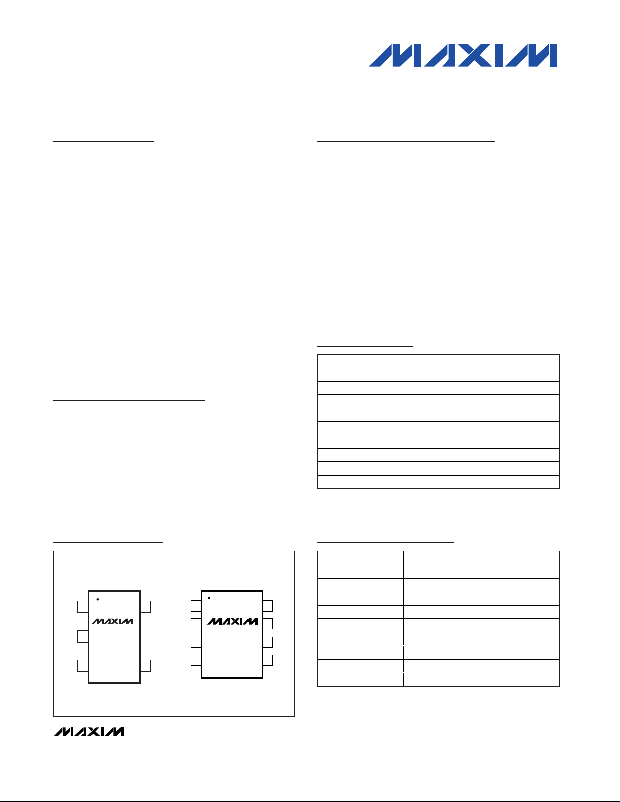
GND
N.C.N.C.
15OUTIN
MAX6029
SOT23
TOP VIEW
2
34
OUT
N.C.GND
1
2
87N.C.
N.C.IN
N.C.
N.C.
SO
3
4
6
5
MAX6029
Pin Configurations
Ordering Information
19-2892; Rev 2; 11/06
For pricing, delivery, and ordering information, please contact Maxim/Dallas Direct! at
1-888-629-4642, or visit Maxim’s website at www.maxim-ic.com.
PART
PIN-PACKAGE
TOP
MARK
PKG
CODE
MAX6029EUK21-T
5 SOT23-5 AEHD U5-1
MAX6029EUK25-T
5 SOT23-5 AEHF U5-1
MAX6029ESA25 8 SO — S8-2
MAX6029EUK30-T
5 SOT23-5 AEHH U5-1
MAX6029EUK33-T
5 SOT23-5 AEHN U5-1
MAX6029EUK41-T
5 SOT23-5 AEHJ U5-1
MAX6029ESA41 8 SO — S8-2
MAX6029EUK50-T
5 SOT23-5 AEHL U5-1
Selector Guide
PART PIN-PACKAGE
OUTPUT
VOLTAGE (V)
MAX6029EUK21-T 5 SOT23-5 2.048
MAX6029EUK25-T 5 SOT23-5 2.500
MAX6029ESA25 8 SO 2.500
MAX6029EUK30-T 5 SOT23-5 3.000
MAX6029EUK33-T 5 SOT23-5 3.300
MAX6029EUK41-T 5 SOT23-5 4.096
MAX6029ESA41 8 SO 4.096
MAX6029EUK50-T 5 SOT23-5 5.000
Note: All devices are specified over the -40°C to +85°C operating temperature range.
Page 2
MAX6029
Ultra-Low-Power Precision Series
Voltage Reference
2 _______________________________________________________________________________________
ABSOLUTE MAXIMUM RATINGS
Stresses beyond those listed under “Absolute Maximum Ratings” may cause permanent damage to the device. These are stress ratings only, and functional
operation of the device at these or any other conditions beyond those indicated in the operational sections of the specifications is not implied. Exposure to
absolute maximum rating conditions for extended periods may affect device reliability.
IN to GND ...............................................................-0.3V to +13V
OUT to GND ..............-0.3V to the lower of +6V and (V
IN
+ 0.3V)
Output to GND Short-Circuit Duration........................Continuous
Continuous Power Dissipation (T
A
= +70°C)
5-Pin SOT23 (derate 7.1mW/°C above +70°C)............571mW
8-Pin SO (derate 5.9mW/°C above +70°C)...............470.6mW
Operating Temperature Range ...........................-40°C to +85°C
Storage Temperature Range .............................-65°C to +150°C
Lead Temperature (soldering, 10s) .................................+300°C
ELECTRICAL CHARACTERISTICS—MAX6029_21 (V
OUT
= 2.048V)
(VIN= 2.5V, I
OUT
= 0, TA= T
MIN
to T
MAX
, unless otherwise noted. Typical values are at TA= +25°C.) (Note 1)
PARAMETER
CONDITIONS
UNITS
OUTPUT
Output Voltage V
OUT
TA = +25°C
V
Output Voltage Temperature
Coefficient
TCV
OUT
(Notes 2, 3) 30
ppm/°C
Line Regulation
VIN = 2.5V to 12.6V 27 200
µV/V
I
OUT
= 0 to 4mA
0.7
Load Regulation
∆V
OUT
/
∆I
OUT I
OUT
= 0 to -1mA 2.4 5.5
µV/µA
Output Short-Circuit Current I
SC
60 mA
Long-Term Stability
1000 hours at +25°C
ppm
Thermal Hysteresis (Note 4)
ppm
DYNAMIC CHARACTERISTICS
f = 0.1Hz to 10Hz 30
µV
P-P
Noise Voltage e
OUT
f = 10Hz to 1kHz
µV
RMS
Ripple Rejection
VIN = 2.5V ±200mV, f = 120Hz 43 dB
Turn-On Settling Time t
R
To V
OUT
= 0.1% of final value
µs
INPUT
Supply Voltage Range V
IN
2.5
V
Supply Current I
IN
µA
Change in Supply Current IIN/V
IN
VIN = 2.5V to 12.6V 1.5
µA/V
SYMBOL
∆V
/∆V
OUT
IN
∆V
/time
OUT
∆V
/∆V
OUT
IN
MIN TYP MAX
2.0449 2.0480 2.0511
0.22
150
140
115
450
12.6
5.25
Page 3
MAX6029
Ultra-Low-Power Precision Series
Voltage Reference
_______________________________________________________________________________________ 3
ELECTRICAL CHARACTERISTICS—MAX6029_25 (V
OUT
= 2.500V)
(VIN= 2.7V, I
OUT
= 0, TA= T
MIN
to T
MAX
, unless otherwise noted. Typical values are at TA= +25°C.) (Note 1)
PARAMETER
SYMBOL
CONDITIONS
MIN
TYP
MAX
UNITS
OUTPUT
MAX6029EUK
Output Voltage V
OUT
TA = +25°C
MAX6029ESA
V
Output Voltage Temperature
Coefficient
TCV
OUT
(Notes 2, 3) 30
ppm/°C
Line Regulation
VIN = 2.7V to 12.6V 30 230
µV/V
I
OUT
= 0 to 4mA 0.1 0.6
Load Regulation
I
OUT
= 0 to -1mA 2.5 6.2
µV/µA
I
OUT
= 0 100
Dropout Voltage (Note 5)
I
OUT
= 4mA 200
mV
Output Short-Circuit Current I
SC
60 mA
Long-Term Stability
1000 hours at +25°C
ppm
Thermal Hysteresis (Note 4)
ppm
DYNAMIC CHARACTERISTICS
f = 0.1Hz to 10Hz 39
µV
P-P
Noise Voltage e
OUT
f = 10Hz to 1kHz
µV
RMS
Ripple Rejection
VIN = 2.7V ±200mV, f = 120Hz 34 dB
Turn-On Settling Time t
R
To V
OUT
= 0.1% of final value
ms
INPUT
Supply Voltage Range V
IN
2.7
V
Supply Current I
IN
µA
Change in Supply Current IIN/V
IN
VIN = 2.7V to 12.6V 1.5
µA/V
∆V
/∆V
OUT
IN
∆V
/∆I
OUT
OUT
VIN - V
OUT
∆V
/time
OUT
∆V
/∆V
OUT
IN
2.4963 2.5000 2.5038
2.495 2.500 2.505
150
140
137
700
12.6
5.75
Page 4
MAX6029
Ultra-Low-Power Precision Series
Voltage Reference
4 _______________________________________________________________________________________
ELECTRICAL CHARACTERISTICS—MAX6029_30 (V
OUT
= 3.000V)
(VIN= 3.2V, I
OUT
= 0, TA= T
MIN
to T
MAX
, unless otherwise noted. Typical values are at TA= +25°C.) (Note 1)
PARAMETER
CONDITIONS
UNITS
OUTPUT
Output Voltage V
OUT
TA = +25°C
V
Output Voltage Temperature
Coefficient
TCV
OUT
(Notes 2, 3) 30
ppm/°C
Line Regulation
VIN = 3.2V to 12.6V 15 250
µV/V
I
OUT
= 0 to 4mA 0.1 0.6
Load Regulation
∆V
OUT
/
∆I
OUT I
OUT
= 0 to -1mA 2.4 6.5
µV/µA
I
OUT
= 0 100
Dropout Voltage (Note 5)
I
OUT
= 4mA 200
mV
Output Short-Circuit Current I
SC
60 mA
Long-Term Stability
1000 hours at +25°C
ppm
Thermal Hysteresis (Note 4)
ppm
DYNAMIC CHARACTERISTICS
f = 0.1Hz to 10Hz 39
µV
P-P
Noise Voltage e
OUT
f = 10Hz to 1kHz
µV
RMS
Ripple Rejection
VIN = 3.2V ±200mV, f = 120Hz 37 dB
Turn-On Settling Time t
R
To V
OUT
= 0.1% of final value
µs
INPUT
Supply Voltage Range V
IN
3.2
V
Supply Current I
IN
µA
Change in Supply Current IIN/V
IN
VIN = 3.2V to 12.6V 1.5
µA/V
SYMBOL
∆V
/∆V
OUT
IN
VIN - V
OUT
∆V
/time
OUT
∆V
/∆V
OUT
IN
MIN TYP MAX
2.9955 3.0000 3.0045
150
140
161
775
12.6
6.75
Page 5
MAX6029
Ultra-Low-Power Precision Series
Voltage Reference
_______________________________________________________________________________________ 5
ELECTRICAL CHARACTERISTICS—MAX6029_33 (V
OUT
= 3.300V)
(VIN= 3.5V, I
OUT
= 0, TA= T
MIN
to T
MAX
, unless otherwise noted. Typical values are at TA= +25°C.) (Note 1)
PARAMETER
SYMBOL
CONDITIONS
MIN
TYP
MAX
UNITS
OUTPUT
Output Voltage V
OUT
TA = +25°C
V
Output Voltage Temperature
Coefficient
TCV
OUT
(Notes 2, 3) 30
ppm/°C
Line Regulation
VIN = 3.5V to 12.6V 30
µV/V
I
OUT
= 0 to 4mA 0.1 0.6
Load Regulation
I
OUT
= 0 to -1mA 2.4 7
µV/µA
I
OUT
= 0
Dropout Voltage (Note 5)
I
OUT
= 4mA
mV
Output Short-Circuit Current I
SC
60 mA
Long-Term Stability
1000 hours at +25°C
ppm
Thermal Hysteresis (Note 4)
ppm
DYNAMIC CHARACTERISTICS
f = 0.1Hz to 10Hz 56
µV
P-P
Noise Voltage e
OUT
f = 10Hz to 1kHz
µV
RMS
Ripple Rejection
VIN = 3.5V ±200mV, f = 120Hz 38 dB
Turn-On Settling Time t
R
To V
OUT
= 0.1% of final value 1 ms
INPUT
Supply Voltage Range V
IN
3.5
V
Supply Current I
IN
µA
Change in Supply Current IIN/V
IN
VIN = 3.5V to 12.6V 1.5
µA/V
∆V
/∆V
OUT
IN
∆V
/∆I
OUT
OUT
VIN - V
OUT
∆V
/time
OUT
∆V
/∆V
OUT
IN
3.2951 3.3000 3.3050
270
100
200
150
140
174
12.6
7.25
Page 6

MAX6029
Ultra-Low-Power Precision Series
Voltage Reference
6 _______________________________________________________________________________________
ELECTRICAL CHARACTERISTICS—MAX6029_41 (V
OUT
= 4.096V)
(VIN= 4.3V, I
OUT
= 0, TA= T
MIN
to T
MAX
, unless otherwise noted. Typical values are at TA= +25°C.) (Note 1)
PARAMETER SYMBOL CONDITIONS
MIN
TYP
MAX
UNITS
OUTPUT
MAX6029EUK
Output Voltage V
OUT
TA = +25°C
MAX6029ESA
4.088
V
Output Voltage Temperature
Coefficient
TCV
OUT
(Notes 2, 3) 30
ppm/°C
Line Regulation
VIN = 4.3V to 12.6V 30 310
µV/V
I
OUT
= 0 to 4mA 0.1 0.6
Load Regulation
I
OUT
= 0 to -1mA 2.5 8.5
µV/µA
I
OUT
= 0 100
Dropout Voltage (Note 5)
I
OUT
= 4mA 200
mV
Output Short-Circuit Current I
SC
60 mA
Long-Term Stability
1000 hours at +25°C
ppm
Thermal Hysteresis (Note 4)
ppm
DYNAMIC CHARACTERISTICS
f = 0.1Hz to 10Hz 72
µV
P-P
Noise Voltage e
OUT
f = 10Hz to 1kHz
µV
RMS
Ripple Rejection
VIN = 4.3V ±200mV, f = 120Hz 36 dB
Turn-On Settling Time t
R
To V
OUT
= 0.1% of final value 1.2 ms
INPUT
Supply Voltage Range V
IN
4.3
V
Supply Current I
IN
µA
Change in Supply Current IIN/V
IN
VIN = 4.3V to 12.6V 1.5
µA/V
∆V
/∆V
OUT
IN
∆V
/∆I
OUT
OUT
VIN - V
OUT
∆V
/time
OUT
∆V
/∆V
OUT
IN
4.0899 4.0960 4.1021
4.096 4.104
150
140
210
12.6
8.75
Page 7

MAX6029
Ultra-Low-Power Precision Series
Voltage Reference
_______________________________________________________________________________________ 7
Note 1: MAX6029 is 100% production tested at TA= +25°C and is guaranteed by design for TA= T
MIN
to T
MAX
as specified.
Note 2: Temperature coefficient is defined by box method: (V
MAX
- V
MIN
)/(∆T ✕V
+25°C
).
Note 3: Not production tested. Guaranteed by design.
Note 4: Thermal hysteresis is defined as the change in T
A
= +25°C output voltage before and after temperature cycling of the
device (from T
A
= T
MIN
to T
MAX
). Initial measurement at TA= +25°C is followed by temperature cycling the device to TA=
+85°C then to TA= -40°C and another measurement at TA= +25°C is compared to the original measurement at TA= +25°C.
Note 5: Dropout voltage is the minimum input voltage at which V
OUT
changes by 0.1% from V
OUT
at rated VINand is guaranteed by
Load Regulation Test.
ELECTRICAL CHARACTERISTICS—MAX6029_50 (V
OUT
= 5.000V)
(VIN= 5.2V, I
OUT
= 0, TA= T
MIN
to T
MAX
, unless otherwise noted. Typical values are at TA= +25°C.) (Note 1)
PARAMETER
SYMBOL
CONDITIONS
MIN
TYP
MAX
UNITS
OUTPUT
Output Voltage V
OUT
TA = +25°C
V
Output Voltage Temperature
Coefficient
TCV
OUT
(Notes 2, 3) 30
ppm/°C
Line Regulation
VIN = 5.2V to 12.6V 34
µV/V
I
OUT
= 0 to 4mA 0.3 0.8
Load Regulation
∆V
OUT
/
∆I
OUT I
OUT
= 0 to -1mA 3.3 9
µV/µA
I
OUT
= 0
Dropout Voltage (Note 5)
I
OUT
= 4mA
mV
Output Short-Circuit Current I
SC
60 mA
Long-Term Stability
1000 hours at +25°C
ppm
Thermal Hysteresis (Note 4)
ppm
DYNAMIC CHARACTERISTICS
f = 0.1Hz to 10Hz 90
µV
P-P
Noise Voltage e
OUT
f = 10Hz to 1kHz
µV
RMS
Ripple Rejection
VIN = 5.2V ±200mV, f = 120Hz 38 dB
Turn-On Settling Time t
R
To V
OUT
= 0.1% of final value 1.4 ms
INPUT
Supply Voltage Range V
IN
5.2
V
Supply Current I
IN
µA
Change in Supply Current IIN/V
IN
VIN = 5.2V to 12.6V 1.5
µA/V
∆V
/∆V
OUT
IN
VIN - V
OUT
∆V
/time
OUT
∆V
/∆V
OUT
IN
4.9925 5.0000 5.0075
375
100
200
150
140
245
12.6
10.5
Page 8
MAX6029
Ultra-Low-Power Precision Series
Voltage Reference
8 _______________________________________________________________________________________
Typical Operating Characteristics
(VIN= 2.5V for MAX6029EUK21, VIN= 3.2V for MAX6029EUK30, and VIN= 5.2V for MAX6029EUK50, I
OUT
= 0, TA= +25°C, unless
otherwise noted.)
OUTPUT VOLTAGE vs. TEMPERATURE
(V
OUT
= 2.048V)
MAX6029 toc01
TEMPERATURE (°C)
OUTPUT VOLTAGE (V)
603510-15
2.042
2.044
2.046
2.048
2.050
2.040
-40 85
3 TYPICAL UNITS
OUTPUT VOLTAGE vs. TEMPERATURE
(V
OUT
= 3V)
MAX6029 toc02
TEMPERATURE (°C)
OUTPUT VOLTAGE (V)
603510-15
2.993
2.995
2.997
2.999
3.001
3.003
2.991
-40 85
3 TYPICAL UNITS
OUTPUT VOLTAGE vs. TEMPERATURE
(V
OUT
= 5V)
MAX6029 toc03
TEMPERATURE (°C)
OUTPUT VOLTAGE (V)
4.990
4.992
4.994
4.996
4.998
5.000
5.002
5.004
5.006
4.988
603510-15-40 85
3 TYPICAL UNITS
SUPPLY CURRENT vs. INPUT VOLTAGE
MAX6029 toc04
INPUT VOLTAGE (V)
SUPPLY CURRENT (µA)
121110987654321
2
4
6
8
10
12
14
0
013
V
OUT
= 3V
V
OUT
= 5V
V
OUT
= 2.048V
SUPPLY CURRENT vs. TEMPERATURE
MAX6029 toc05
TEMPERATURE (°C)
SUPPLY CURRENT (µA)
603510-15
3.0
3.5
4.0
4.5
5.0
5.5
6.0
6.5
7.0
2.5
-40 85
V
OUT
= 3V
V
OUT
= 5V
V
OUT
= 2.048V
DROPOUT VOLTAGE vs. SOURCE CURRENT
(V
OUT
= 2.048V)
MAX6029 toc06
SOURCE CURRENT (mA)
DROPOUT VOLTAGE (V)
651 2 3 4
0.02
0.04
0.06
0.08
0.10
0.12
0.14
0.16
0
07
DROPOUT VOLTAGE vs. SOURCE CURRENT
(V
OUT
= 3V)
MAX6029 toc07
SOURCE CURRENT (mA)
DROPOUT VOLTAGE (V)
653 421
0.01
0.02
0.03
0.04
0.05
0.06
0.07
0.08
0.09
0.10
0.11
0
07
DROPOUT VOLTAGE vs. SOURCE CURRENT
(V
OUT
= 5V)
MAX6029 toc08
SOURCE CURRENT (mA)
DROPOUT VOLTAGE (V)
653 421
0.01
0.02
0.03
0.04
0.05
0.06
0.07
0.08
0.09
0
07
LOAD REGULATION
(V
OUT
= 2.048V)
MAX6029 toc09
OUTPUT CURRENT (mA)
OUTPUT VOLTAGE (V)
653 40 1 2-1
2.0475
2.0480
2.0485
2.0490
2.0495
2.0500
2.0505
2.0510
2.0515
2.0520
2.0470
-2 7
Page 9

MAX6029
Ultra-Low-Power Precision Series
Voltage Reference
_______________________________________________________________________________________ 9
LINE REGULATION
(V
OUT
= 2.048V)
MAX6029 toc10
INPUT VOLTAGE (V)
OUTPUT VOLTAGE (V)
11.510.07.0 8.55.54.0
2.04774
2.04776
2.04778
2.04780
2.04782
2.04784
2.04786
2.04788
2.04790
2.04792
2.04772
2.5 13.0
LOAD REGULATION
(V
OUT
= 3V)
MAX6029 toc11
OUTPUT CURRENT (mA)
OUTPUT VOLTAGE (V)
653 40 1 2-1
3.0015
3.0020
3.0025
3.0030
3.0035
3.0040
3.0045
3.0050
3.0055
3.0010
-2 7
LINE REGULATION
(V
OUT
= 3V)
MAX6029 toc12
INPUT VOLTAGE (V)
OUTPUT VOLTAGE (V)
121110987654
3.00160
3.00165
3.00170
3.00175
3.00180
3.00155
313
LOAD REGULATION
(V
OUT
= 5V)
MAX6029 toc13
OUTPUT CURRENT (mA)
OUTPUT VOLTAGE (V)
653 40 1 2-1
5.0015
5.0020
5.0025
5.0030
5.0035
5.0040
5.0045
5.0050
5.0005
5.0010
-2 7
LINE REGULATION
(V
OUT
= 5V)
MAX6029 toc14
INPUT VOLTAGE (V)
OUTPUT VOLTAGE (V)
12116 7 8 9 10
5.00066
5.00068
5.00070
5.00072
5.00074
5.00076
5.00078
5.00080
5.00064
513
POWER-SUPPLY REJECTION RATIO vs.
FREQUENCY (V
OUT
= 2.048V)
MAX6029 toc15
FREQUENCY (kHz)
PSRR (dB)
100101
-50
-40
-30
-20
-10
0
-60
0.1 1000
POWER-SUPPLY REJECTION RATIO
vs. FREQUENCY (V
OUT
= 3V)
MAX6029 toc16
FREQUENCY (kHz)
PSRR (dB)
100101
-50
-40
-30
-20
-10
0
-60
0.1 1000
POWER-SUPPLY REJECTION RATIO
vs. FREQUENCY (V
OUT
= 5V)
MAX6029 toc17
FREQUENCY (kHz)
PSRR (dB)
100101
-45
-40
-35
-30
-25
-20
-15
-10
-5
0
-50
0.1 1000
Typical Operating Characteristics (continued)
(VIN= 2.5V for MAX6029EUK21, VIN= 3.2V for MAX6029EUK30, and VIN= 5.2V for MAX6029EUK50, I
OUT
= 0, TA= +25°C, unless
otherwise noted.)
LINE-TRANSIENT RESPONSE
(V
OUT
= 2.048V)
MAX6029 toc18
200µs/div
3V
2.5V
2.048V
V
IN
200mV/div
AC-COUPLED
V
OUT
200mV/div
AC-COUPLED
Page 10

MAX6029
Ultra-Low-Power Precision Series
Voltage Reference
10 ______________________________________________________________________________________
LINE-TRANSIENT RESPONSE
(V
OUT
= 3V)
MAX6029 toc19
200µs/div
3.7V
3.2V
3V
V
IN
200mV/div
AC-COUPLED
V
OUT
200mV/div
AC-COUPLED
LINE-TRANSIENT RESPONSE
(V
OUT
= 5V)
MAX61029 toc20
200µs/div
5.7V
5.2V
5V
V
IN
200mV/div
AC-COUPLED
V
OUT
100mV/div
AC-COUPLED
LOAD-TRANSIENT RESPONSE
(SOURCING, V
OUT
= 2.048V)
MAX6029 toc21
100µs/div
4mA
2.048V
I
OUT
10mA/div
V
OUT
500mV/div
AC-COUPLED
C
OUT
= 0
0
LOAD-TRANSIENT RESPONSE
(SINKING, V
OUT
= 2.048V)
MAX6029 toc22
1ms/div
0
-1mA
2.048V
I
OUT
2mA/div
V
OUT
500mV/div
AC-COUPLED
C
OUT
= 0
LOAD-TRANSIENT RESPONSE
(SOURCING, V
OUT
= 2.048V)
MAX6029 toc23
400µs/div
4mA
2.048V
I
OUT
10mA/div
V
OUT
500mV/div
AC-COUPLED
C
OUT
= 1µF
0
LOAD-TRANSIENT RESPONSE
(SINKING, V
OUT
= 2.048V)
MAX6029 toc24
1ms/div
0
-1mA
2.048V
I
OUT
2mA/div
V
OUT
500mV/div
AC-COUPLED
C
OUT
= 1µF
Typical Operating Characteristics (continued)
(VIN= 2.5V for MAX6029EUK21, VIN= 3.2V for MAX6029EUK30, and VIN= 5.2V for MAX6029EUK50, I
OUT
= 0, TA= +25°C, unless
otherwise noted.)
Page 11

MAX6029
Ultra-Low-Power Precision Series
Voltage Reference
______________________________________________________________________________________ 11
LOAD-TRANSIENT RESPONSE
(SINKING, V
OUT
= 5V)
MAX6029 toc28
2ms/div
0
-1mA
5V
I
OUT
1mA/div
V
OUT
1V/div
AC-COUPLED
C
OUT
= 1µF
TURN-ON TRANSIENT
(V
OUT
= 2.048V)
MAX6029 toc29
200µs/div
2.5V
2.048V
V
IN
1V/div
V
OUT
1V/div
0
0
TURN-ON TRANSIENT
(V
OUT
= 3V)
MAX6029 toc30
200µs/div
3.2V
3V
V
IN
2V/div
V
OUT
1V/div
0
0
LOAD-TRANSIENT RESPONSE
(SOURCING, V
OUT
= 5V)
MAX6029 toc25
400µs/div
4mA
5V
I
OUT
10mA/div
V
OUT
500mV/div
AC-COUPLED
C
OUT
= 0
0
LOAD-TRANSIENT RESPONSE
(SINKING, V
OUT
= 5V)
MAX6029 toc26
2ms/div
0
-1mA
5V
I
OUT
1mA/div
V
OUT
1V/div
AC-COUPLED
C
OUT
= 0
LOAD-TRANSIENT RESPONSE
(SOURCING, V
OUT
= 5V)
6029 toc27
400µs/div
4mA
6V
I
OUT
10mA/div
V
OUT
200mV/div
AC-COUPLED
C
OUT
= 1µF
0
Typical Operating Characteristics (continued)
(VIN= 2.5V for MAX6029EUK21, VIN= 3.2V for MAX6029EUK30, and VIN= 5.2V for MAX6029EUK50, I
OUT
= 0, TA= +25°C, unless
otherwise noted.)
Page 12

MAX6029
Ultra-Low-Power Precision Series
Voltage Reference
12 ______________________________________________________________________________________
NOISE vs. FREQUENCY
(V
OUT
= 5V)
MAX6029 toc37
FREQUENCY (kHz)
NOISE (µV
RMS
/√Hz)
40302010
2
4
6
8
10
12
14
16
18
20
0
050
Typical Operating Characteristics (continued)
(VIN= 2.5V for MAX6029EUK21, VIN= 3.2V for MAX6029EUK30, and VIN= 5.2V for MAX6029EUK50, I
OUT
= 0, TA= +25°C, unless
otherwise noted.)
0.1Hz TO 10Hz OUTPUT NOISE
(V
OUT
= 5V)
MAX6029 toc34
1s/div
V
OUT
20µV/div
NOISE vs. FREQUENCY
(V
OUT
= 2.048V)
MAX6029 toc35
FREQUENCY (kHz)
NOISE (µV
RMS
/√Hz)
403010 20
0.5
1.0
1.5
2.0
2.5
3.0
3.5
4.0
0
050
NOISE vs. FREQUENCY
(V
OUT
= 3V)
MAX6029 toc36
FREQUENCY (kHz)
NOISE (µV
RMS
/√Hz)
40302010
0.5
1.0
1.5
2.0
2.5
3.0
3.5
4.0
4.5
5.0
5.5
6.0
6.5
0
050
0.1Hz TO 10Hz OUTPUT NOISE
(V
OUT
= 2.048V)
MAX6029 toc32
1s/div
V
OUT
10µV/div
0.1Hz TO 10Hz OUTPUT NOISE
(V
OUT
= 3V)
MAX6029 toc33
1s/div
V
OUT
10µV/div
TURN-ON TRANSIENT
(V
OUT
= 5V)
MAX6029 toc31
400µs/div
5.2V
5V
V
IN
2V/div
V
OUT
2V/div
0
0
Page 13
MAX6029
Ultra-Low-Power Precision Series
Voltage Reference
______________________________________________________________________________________ 13
Applications Information
Input Bypassing
The MAX6029 does not require an input bypass capacitor. For improved transient performance, bypass the
input to ground with a 0.1µF ceramic capacitor. Place
the capacitor as close to IN as possible.
Load Capacitance
The MAX6029 does not require an output capacitor for
stability. The MAX6029 is stable driving capacitive
loads from 0 to 100pF and 0.1µF to 10µF when sourcing current and from 0 to 0.4µF when sinking current. In
applications where the load or the supply can experience step changes, an output capacitor reduces the
amount of overshoot (undershoot) and improves the circuit’s transient response. Many applications do not
require an external capacitor, and the MAX6029 offers
a significant advantage in applications where board
space is critical.
Supply Current
The quiescent supply current of the series-mode
MAX6029 is very small, 5.25µA (max), and is very stable against changes in the supply voltage with only
1.5µA/V (max) variation with supply voltage. The
MAX6029 family draws load current from the input voltage source only when required, so supply current is not
wasted and efficiency is maximized at all input voltages. This improved efficiency reduces power dissipation and extends battery life.
Output Thermal Hysteresis
Output thermal hysteresis is the change of the output
voltage at T
A
= +25°C before and after the device is
cycled over its entire operating temperature range.
Hysteresis is caused by differential package stress
appearing across the device.
Temperature Coefficient vs. Operating
Temperature Range for a 1LSB
Maximum Error
In a data converter application, the reference voltage of
the converter must stay within a certain limit to keep the
error in the data converter smaller than the resolution
limit through the operating temperature range. Figure 1
shows the maximum allowable reference voltage temperature coefficient to keep the conversion error to less than
1 LSB, as a function of the operating temperature range
(T
MAX
- T
MIN
) with the converter resolution as a parameter. The graph assumes the reference-voltage temperature coefficient as the only parameter affecting accuracy.
In reality, the absolute static accuracy of a data converter is dependent on the combination of many parameters
such as integral nonlinearity, differential nonlinearity, offset error, gain error, as well as voltage reference
changes.
Turn-On Time
These devices turn on and settle to within 0.1% of their
final value in less than 1ms. The turn-on time increases
when heavily loaded and operating close to dropout.
Pin Description
PIN
SOT23
SO
NAME
FUNCTION
12IN Positive Voltage Supply
24GND Ground
3, 4
1, 3, 5, 7,
8
N.C.
No Connection. Leave
unconnected or connect to
ground.
56OUT Reference Output
Figure 1. Temperature Coefficient vs. Operating Temperature Range for a 1 LSB Maximum Error
10,000
1000
100
TEMPERATURE
COEFFICIENT
(ppm/°C)
10
1
0.1
0.01
110
OPERATING TEMPERATURE RANGE (T
MAX
8-BIT
10-BIT
12-BIT
14-BIT
16-BIT
18-BIT
20-BIT
- T
) (°C)
MIN
100
Page 14
MAX6029
Ultra-Low-Power Precision Series
Voltage Reference
14 ______________________________________________________________________________________
OUT
GND
IN
MAX6029
VIN = 2.5V TO 12.6V
*CAPACITOR IS OPTIONAL.
*
Typical Operating Circuit
Chip Information
TRANSISTOR COUNT: 30
PROCESS: BiCMOS
Page 15

MAX6029
Ultra-Low-Power Precision Series
Voltage Reference
______________________________________________________________________________________ 15
Package Information
(The package drawing(s) in this data sheet may not reflect the most current specifications. For the latest package outline information,
go to www.maxim-ic.com/packages.)
SOT-23 5L .EPS
Page 16

MAX6029
Ultra-Low-Power Precision Series
Voltage Reference
Maxim cannot assume responsibility for use of any circuitry other than circuitry entirely embodied in a Maxim product. No circuit patent licenses are
implied. Maxim reserves the right to change the circuitry and specifications without notice at any time.
16 ____________________Maxim Integrated Products, 120 San Gabriel Drive, Sunnyvale, CA 94086 408-737-7600
© 2006 Maxim Integrated Products is a registered trademark of Maxim Integrated Products, Inc.
Package Information (continued)
(The package drawing(s) in this data sheet may not reflect the most current specifications. For the latest package outline information,
go to www.maxim-ic.com/packages.)
SOICN .EPS
PACKAGE OUTLINE, .150" SOIC
1
1
21-0041
B
REV.DOCUMENT CONTROL NO.APPROVAL
PROPRIETARY INFORMATION
TITLE:
TOP VIEW
FRONT VIEW
MAX
0.010
0.069
0.019
0.157
0.010
INCHES
0.150
0.007
E
C
DIM
0.014
0.004
B
A1
MIN
0.053A
0.19
3.80 4.00
0.25
MILLIMETERS
0.10
0.35
1.35
MIN
0.49
0.25
MAX
1.75
0.050
0.016L
0.40 1.27
0.3940.386D
D
MINDIM
D
INCHES
MAX
9.80 10.00
MILLIMETERS
MIN
MAX
16
AC
0.337 0.344 AB8.758.55 14
0.189 0.197 AA5.004.80 8
N MS012
N
SIDE VIEW
H 0.2440.228 5.80 6.20
e 0.050 BSC 1.27 BSC
C
HE
e
B
A1
A
D
0∞-8∞
L
1
VARIATIONS:
Revision History
Pages changed at Rev 1: 1, 2, 13, 15, 16
Pages changed at Rev 2: 1, 3, 6, 16
 Loading...