

Page 1
General Description
The MAX6023 is a family of low-dropout, micropower
voltage references in a 5-bump, chip-scale package
(UCSP™). The MAX6023 series-mode (three-terminal)
references, which operate with input voltages from 2.5V
to 12.6V (1.25V and 2.048V options) or (V
OUT
+ 0.2V) to
12.6V (all other voltage options), are available with output voltage options of 1.25V, 2.048V, 2.5V, 3.0V,
4.096V, 4.5V, and 5.0V. These devices are guaranteed
an initial accuracy of ±0.2% and 30ppm/°C temperature drift over the -40°C to +85°C extended temperature
range.
UCSPs offer the benefit of moving to smaller footprint
and lower profile devices, significantly smaller than even
SC70 or SOT23 plastic surface-mount packages. The
significantly lower profile (compared to plastic SMD
packages) of the UCSP makes the device ideal for
height-critical applications. Miniature UCSP packages
also enable device placement close to sources and
allow more flexibility in a complex or large design layout.
The MAX6023 voltage references use only 27µA of supply current. And unlike shunt-mode (two-terminal) references, the supply current of the MAX6023 family varies
only 0.8µA/V with supply-voltage changes, translating to
longer battery life. Additionally, these internally compensated devices do not require an external compensation
capacitor and are stable up to 2.2nF of load capacitance. The low-dropout voltage and the low supply current make these devices ideal for battery-operated
systems.
Applications
Hand-Held Equipment
Data Acquisition Systems
Industrial and Process Control Systems
Battery-Operated Equipment
Hard-Disk Drives
Features
♦ 5-Bump UCSP Package (1.0mm ✕ 1.5mm ✕ 0.3mm)
♦ No Output Capacitor Needed
♦ ±0.2% (max) Initial Accuracy
♦ 30ppm/°C (max) Temperature Coefficient
♦ 35µA (max) Quiescent Supply Current
♦ 0.8µA/V (max) Supply Current Variation with V
IN
♦ 100mV Dropout at 500µA Load Current
♦ Line Regulation: 160µV/V (max)
♦ Output Voltage Options: 1.25V, 2.048V, 2.5V, 3.0V,
4.096V, 4.5V, 5.0V
MAX6023
Precision, Low-Power, Low-Dropout, UCSP
Voltage Reference
________________________________________________________________ Maxim Integrated Products 1
Ordering Information
MAX6023
*
*CAPACITOR IS OPTIONAL.
REFERENCE
OUT
OUT
IN
GND
+SUPPLY INPUT (SEE SELECTOR GUIDE)
Typical Operating Circuit
19-2182; Rev 2; 12/02
For pricing, delivery, and ordering information, please contact Maxim/Dallas Direct! at
1-888-629-4642, or visit Maxim’s website at www.maxim-ic.com.
UCSP is a trademark of Maxim Integrated Products, Inc.
PART
BUMP-
TOP
MARK
MAX6023EBT12-T
AAO
MAX6023EBT21-T
AAT
MAX6023EBT25-T
AAP
MAX6023EBT30-T
AAS
MAX6023EBT41-T
AAQ
MAX6023EBT45-T
AAR
MAX6023EBT50-T
AAU
Pin Configuration appears at end of data sheet.
*UCSP reliability is integrally linked to the user’s assembly methods, circuit board material, and environment. See the UCSP
Reliability Notice in the UCSP Reliability section of this data sheet
for more information.
PART
INPUT VOLTAGE (V)
MAX6023EBT12
1.250 2.5V to 12.6
MAX6023EBT21
2.048 2.5V to 12.6
MAX6023EBT25
2.500 (V
OUT
+ 200mV) to 12.6
MAX6023EBT30
3.000 (V
OUT
+ 200mV) to 12.6
MAX6023EBT41
4.096 (V
OUT
+ 200mV) to 12.6
MAX6023EBT45
4.500 (V
OUT
+ 200mV) to 12.6
MAX6023EBT50
5.000 (V
OUT
+ 200mV) to 12.6
Selector Guide
TEMP RANGE
-40°C to +85°C 5 UCSP*-5
-40°C to +85°C 5 UCSP-5
-40°C to +85°C 5 UCSP-5
-40°C to +85°C 5 UCSP-5
-40°C to +85°C 5 UCSP-5
-40°C to +85°C 5 UCSP-5
-40°C to +85°C 5 UCSP-5
PACKAGE
V
(V)
OUT
Page 2
MAX6023
Precision, Low-Power, Low-Dropout, UCSP
Voltage Reference
2 _______________________________________________________________________________________
ABSOLUTE MAXIMUM RATINGS
ELECTRICAL CHARACTERISTICS–MAX6023EBT12 (V
OUT
= 1.250V)
(VIN= +5V, I
OUT
= 0, TA= T
MIN
to T
MAX
, unless otherwise noted. Typical values are at TA= +25°C.) (Note 2)
Stresses beyond those listed under “Absolute Maximum Ratings” may cause permanent damage to the device. These are stress ratings only, and functional
operation of the device at these or any other conditions beyond those indicated in the operational sections of the specifications is not implied. Exposure to
absolute maximum rating conditions for extended periods may affect device reliability.
(Voltages Referenced to GND)
IN .........................................................................-0.3V to +13.5V
OUT .............................................................-0.3V to (VIN+ 0.3V)
Output Short Circuit to GND or IN (VIN< 6V) ............Continuous
Output Short Circuit to GND or IN (VIN≥ 6V) .........................60s
Continuous Power Dissipation (TA= +70°C)
5-Bump UCSP (derate 3.4mW/°C above +70°C)........273mW
Operating Temperature Range ..........................-40°C to +85°C
Storage Temperature Range .............................-65°C to +150°C
Bump Temperature (soldering, 10s)................................+300°C
PARAMETER
CONDITIONS
UNITS
OUTPUT
Output Voltage V
OUT
TA = +25°C
V
Initial Voltage Accuracy TA = +25°C
%
Output Voltage Temperature
Coefficient
(Note 3) 10 30
ppm/°C
Line Regulation
∆V
OUT
/
∆V
IN
2.5V ≤ VIN ≤ 12.6V 10 80
µV/V
0 ≤ I
OUT
≤ 400µA 0.4 1.0
Load Regulation
∆V
OUT
/
∆I
OUT
-400µA ≤ I
OUT
≤ 0 0.5 1.1
µV/µA
Short to GND 4
Short-Circuit Current I
SC
Short to IN 10
mA
Temperature Hysteresis (Note 4) 90
ppm
Long-Term Stability
time
1000hr at T
A
= +25°C30
ppm/
1000hr
DYNAMIC CHARACTERISTICS
f = 0.1Hz to 10Hz 25
µVp-p
Noise Voltage e
OUT
f = 10Hz to 10kHz 65
µV
RMS
Ripple Rejection
∆V
OUT
/
∆I
OUT
VIN = +5V ±100mV, f = 120Hz 86 dB
Turn-On Settling Time t
R
To V
OUT
within 0.1% of final value,
C
OUT
= 50pF
30 µs
Capacitive-Load Stability Range
C
OUT
(Note 3) 0 2.2 nF
INPUT
Supply-Voltage Range V
IN
Guaranteed by line-regulation test 2.5
V
Supply Current I
IN
27 35 µA
Change in Supply Current
2.5V ≤ VIN ≤ 12.6V 0.8 2.0
µA/V
Note 1: This device is constructed using a unique set of packaging techniques that impose a limit on the thermal profile the device
can be exposed to during board-level solder attach and rework. This limit permits only the use of solder profiles recommended in the industry-standard specification, JEDEC 020A, paragraph 7.6, Table 3 for IR/VPR and convection reflow.
Preheating is required. Hand or wave soldering is not allowed.
SYMBOL
∆V
/
OUT
MIN TYP MAX
1.247 1.250 1.253
-0.24 +0.24
∆IIN/∆V
IN
12.6
Page 3
MAX6023
Precision, Low-Power, Low-Dropout, UCSP
Voltage Reference
_______________________________________________________________________________________ 3
ELECTRICAL CHARACTERISTICS–MAX6023EBT21 (V
OUT
= 2.048V)
(VIN= +5V, I
OUT
= 0, TA= T
MIN
to T
MAX
, unless otherwise noted. Typical values are at TA= +25°C.) (Note 2)
PARAMETER
CONDITIONS
UNITS
OUTPUT
Output Voltage V
OUT
TA = +25°C
V
Initial Voltage Accuracy TA = +25°C
%
Output Voltage Temperature
Coefficient
(Note 3) 10 30
ppm/°C
Line Regulation
∆V
OUT
/
∆V
IN
2.5V ≤ VIN ≤ 12.6V 20
µV/V
0 ≤ I
OUT
≤ 500µA 0.5 1.4
Load Regulation
∆V
OUT
/
∆I
OUT
-500µA ≤ I
OUT
≤ 0 0.3
µV/µA
Short to GND 4
Short-Circuit Current I
SC
Short to IN 10
mA
Temperature Hysteresis (Note 4) 90
ppm
Long-Term Stability
time
1000hr at T
A
= +25°C50
ppm/
1000hr
DYNAMIC CHARACTERISTICS
f = 0.1Hz to 10Hz 40
µVp-p
Noise Voltage e
OUT
f = 10Hz to 10kHz
µV
RMS
Ripple Rejection
∆V
OUT
/
∆I
OUT
VIN = +5V ±100mV, f = 120Hz 82 dB
Turn-On Settling Time t
R
To V
OUT
within 0.1% of final value,
C
OUT
= 50pF
85 µs
Capacitive-Load Stability Range
C
OUT
(Note 3) 0 2.2 nF
INPUT
Supply-Voltage Range V
IN
Guaranteed by line-regulation test 2.5
V
Supply Current I
IN
27 35 µA
Change in Supply Current
2.5V ≤ VIN ≤ 12.6V 0.8 2.0
µA/V
SYMBOL
∆V
/
OUT
MIN TYP MAX
2.044 2.048 2.052
-0.20 +0.20
100
0.70
105
∆IIN/∆V
IN
12.6
Page 4
MAX6023
Precision, Low-Power, Low-Dropout, UCSP
Voltage Reference
4 _______________________________________________________________________________________
ELECTRICAL CHARACTERISTICS–MAX6023EBT25 (V
OUT
= 2.500V)
(VIN= +5V, I
OUT
= 0, TA= T
MIN
to T
MAX
, unless otherwise noted. Typical values are at TA= +25°C.) (Note 2)
PARAMETER
CONDITIONS
UNITS
OUTPUT
Output Voltage V
OUT
TA = +25°C
2.5
V
Initial Voltage Accuracy TA = +25°C
%
Output Voltage Temperature
Coefficient
(Note 3) 10 30
ppm/°C
Line Regulation
∆V
OUT
/
∆V
IN
(V
OUT
+ 0.2V) ≤ VIN ≤ 12.6V 25
µV/V
0 ≤ I
OUT
≤ 500µA 0.5 1.4
Load Regulation
∆V
OUT
/
∆I
OUT
-500µA ≤ I
OUT
≤ 0 0.3 0.8
µV/µA
Short to GND 4
Short-Circuit Current I
SC
Short to IN 10
mA
Dropout Voltage
I
OUT
= 500µA (Note 5)
mV
Temperature Hysteresis (Note 4) 90
ppm
Long-Term Stability
time
1000hr at T
A
= +25°C50
ppm/
1000hr
DYNAMIC CHARACTERISTICS
f = 0.1Hz to 10Hz 60
µVp-p
Noise Voltage e
OUT
f = 10Hz to 10kHz
µV
RMS
Ripple Rejection
∆V
OUT
/
∆I
OUT
VIN = +5V ±100mV, f = 120Hz 82 dB
Turn-On Settling Time t
R
To V
OUT
within 0.1% of final value,
C
OUT
= 50pF
85 µs
Capacitive-Load Stability Range
C
OUT
(Note 3) 0 2.2 nF
INPUT
Supply-Voltage Range V
IN
Guaranteed by line-regulation test
V
OUT
V
Supply Current I
IN
27 35 µA
Change in Supply Current
(V
OUT
+ 0.2V) ≤ VIN ≤ 12.6V 0.8 2.0
µA/V
SYMBOL
( V
- V
IN
OU T)
∆V
/
OUT
∆IIN/∆V
IN
MIN TYP MAX
2.495
-0.20 +0.20
100 200
125
+ 0.2
2.505
140
12.6
Page 5

MAX6023
Precision, Low-Power, Low-Dropout, UCSP
Voltage Reference
_______________________________________________________________________________________ 5
ELECTRICAL CHARACTERISTICS–MAX6023EBT30 (V
OUT
= 3.000V)
(VIN= +5V, I
OUT
= 0, TA= T
MIN
to T
MAX
, unless otherwise noted. Typical values are at TA= +25°C.) (Note 2)
PARAMETER
CONDITIONS
UNITS
Output Voltage V
OUT
TA = +25°C
V
Initial Voltage Accuracy TA = +25°C
%
Output Voltage Temperature
Coefficient
(Note 3) 10 30
ppm/°C
Line Regulation
∆V
OUT
/
∆V
IN
(V
OUT
+ 0.2V) ≤ VIN ≤ 12.6V 40
µV/V
0 ≤ I
OUT
≤ 500µA 0.7 1.5
Load Regulation
∆V
OUT
/
∆I
OUT
-500µA ≤ I
OUT
≤ 0 0.4 0.8
µV/µA
Dropout Voltage
(V
IN
I
OUT
= 500µA (Note 5)
mV
Short to GND 4
Short-Circuit Current I
SC
Short to IN 10
mA
Temperature Hysteresis (Note 4) 90
ppm
Long-Term Stability
time
1000hr at T
A
= +25°C50
ppm/
1000hr
DYNAMIC CHARACTERISTICS
f = 0.1Hz to 10Hz 75
µVp-p
Noise Voltage e
OUT
f = 10Hz to 10kHz
µV
RMS
Ripple Rejection
∆V
OUT
/
∆V
IN
VIN = +5V ±100mV, f = 120Hz 82 dB
Turn-On Settling Time t
R
To V
OUT
within 0.1% of final value,
C
OUT
= 50pF
85 µs
Capacitive-Load Stability Range
C
OUT
(Note 3) 0 2.2 nF
INPUT
Supply-Voltage Range V
IN
Guaranteed by line-regulation test
V
OUT
V
Supply Current I
IN
27 35 µA
Change in Supply Current
(V
OUT
+ 0.2V) ≤ VIN ≤ 12.6V 0.8 2.0
µA/V
SYMBOL
V
)
OUT
∆V
/
OUT
∆IIN/∆V
IN
MIN TYP MAX
2.994 3.000 3.006
-0.20 +0.20
140
100 200
150
+ 0.2
12.6
Page 6
MAX6023
Precision, Low-Power, Low-Dropout, UCSP
Voltage Reference
6 _______________________________________________________________________________________
ELECTRICAL CHARACTERISTICS–MAX6023EBT41 (V
OUT
= 4.096V)
(VIN= +5V, I
OUT
= 0, TA= T
MIN
to T
MAX
, unless otherwise noted. Typical values are at TA= +25°C.) (Note 2)
PARAMETER
CONDITIONS
UNITS
OUTPUT
Output Voltage V
OUT
TA = +25°C
V
Initial Voltage Accuracy TA = +25°C
%
Output Voltage Temperature
Coefficient
(Note 3) 10 30
ppm/°C
Line Regulation
∆V
OUT
/
∆V
IN
(V
OUT
+ 0.2V) ≤ VIN ≤ 12.6V 50
µV/V
0 ≤ I
OUT
≤ 500µA 1.0 1.8
Load Regulation
∆V
OUT
/
∆I
OUT
-500µA ≤ I
OUT
≤ 0 0.3 0.9
µV/µA
Dropout Voltage
(V
IN
I
OUT
= 500µA (Note 5)
mV
Short to GND 4
Short-Circuit Current I
SC
Short to IN 10
mA
Temperature Hysteresis (Note 4) 90
ppm
Long-Term Stability
time
1000hr at T
A
= +25°C50
ppm/
1000hr
DYNAMIC CHARACTERISTICS
f = 0.1Hz to 10Hz
µVp-p
Noise Voltage e
OUT
f = 10Hz to 10kHz
µV
RMS
Ripple Rejection
∆V
OUT
/
∆V
IN
VIN = +5V ±100mV, f = 120Hz 77 dB
Turn-On Settling Time t
R
To V
OUT
within 0.1% of final value,
C
OUT
= 50pF
µs
Capacitive-Load Stability Range
C
OUT
(Note 3) 0 2.2 nF
INPUT
Supply-Voltage Range V
IN
Guaranteed by line-regulation test
V
OUT
V
Supply Current I
IN
27 35 µA
Change in Supply Current
(V
OUT
+ 0.2V) ≤ VIN ≤ 12.6V 0.8 2.0
µA/V
SYMBOL
V
)
OUT
∆V
/
OUT
∆IIN/∆V
IN
MIN TYP MAX
4.088 4.096 4.104
-0.20 +0.20
160
100 200
100
200
160
+ 0.2
12.6
Page 7

MAX6023
Precision, Low-Power, Low-Dropout, UCSP
Voltage Reference
_______________________________________________________________________________________ 7
ELECTRICAL CHARACTERISTICS–MAX6023EBT45 (V
OUT
= 4.500V)
(VIN= +5V, I
OUT
= 0, TA= T
MIN
to T
MAX
, unless otherwise noted. Typical values are at TA= +25°C.) (Note 2)
PARAMETER
CONDITIONS
UNITS
OUTPUT
Output Voltage V
OUT
TA = +25°C
V
Initial Voltage Accuracy TA = +25°C
%
Output Voltage Temperature
Coefficient
(Note 3) 10 30
ppm/°C
Line Regulation
∆V
OUT
/
∆V
IN
(V
OUT
+ 0.2V) ≤ VIN ≤ 12.6V 50
µV/V
0 ≤ I
OUT
≤ 500µA 1.0 2.0
Load Regulation
∆V
OUT
/
∆I
OUT
-500µA ≤ I
OUT
≤ 0 0.3 1.0
µV/µA
Dropout Voltage
(V
IN
-
I
OUT
= 500µA (Note 5)
mV
Short to GND 4
Short-Circuit Current I
SC
Short to IN 10
mA
Temperature Hysteresis (Note 4) 90
ppm
Long-Term Stability
time
1000hr at T
A
= +25°C50
ppm/
1000hr
DYNAMIC CHARACTERISTICS
f = 0.1Hz to 10Hz
µVp-p
Noise Voltage e
OUT
f = 10Hz to 10kHz
µV
RMS
Ripple Rejection
∆V
OUT
/
∆V
IN
VIN = +5V ±100mV, f = 120Hz 82 dB
Turn-On Settling Time t
R
To V
OUT
within 0.1% of final value,
C
OUT
= 50pF
85 µs
Capacitive-Load Stability Range
C
OUT
(Note 3) 0 2.2 nF
INPUT
Supply-Voltage Range V
IN
Guaranteed by line-regulation test
V
OUT
V
Quiescent Supply Current I
IN
27 35 µA
Change in Supply Current
(V
OUT
+ 0.2V) ≤ VIN ≤ 12.6V 0.8 2.0
µA/V
SYMBOL
V
)
OUT
∆V
/
OUT
∆IIN/∆V
IN
MIN TYP MAX
4.491 4.500 4.509
-0.20 +0.20
160
100 200
110
215
+ 0.2
12.6
Page 8

Note 2: Devices are 100% production tested at TA= +25°C and are guaranteed by design from TA= T
MIN
to T
MAX
.
Note 3: Guaranteed by design.
Note 4: Temperature hysteresis is defined as the change in T
A
= +25°C output voltage before and after temperature cycling of the
device from T
A
= T
MIN
to T
MAX
.
Note 5: Dropout voltage is the minimum input voltage at which V
OUT
changes ≤ 0.2% from V
OUT
at VIN= +5.0V (VIN= +5.5V for
MAX6023EBT50).
MAX6023
Precision, Low-Power, Low-Dropout, UCSP
Voltage Reference
8 _______________________________________________________________________________________
ELECTRICAL CHARACTERISTICS–MAX6023EBT50 (V
OUT
= 5.000V)
(VIN= +5.5V, I
OUT
= 0, TA= T
MIN
to T
MAX
, unless otherwise noted. Typical values are at TA= +25°C.) (Note 2)
PARAMETER
CONDITIONS
UNITS
Output Voltage V
OUT
TA = +25°C
5.0
V
Initial Voltage Accuracy TA = +25°C
%
Output Voltage Temperature
Coefficient
(Note 3) 10 30
ppm/°C
Line Regulation
∆V
OUT
/
∆V
IN
(V
OUT
+ 0.2V) ≤ VIN ≤ 12.6V 50
µV/V
0 ≤ I
OUT
≤ 500µA 1.2 2.2
Load Regulation
∆V
OUT
/
∆I
OUT
-500µA ≤ I
OUT
≤ 0 0.3 1.1
µV/µA
Dropout Voltage
(V
IN
I
OUT
= 500µA (Note 5)
mV
Short to GND 4
Short-Circuit Current I
SC
Short to IN 10
mA
Temperature Hysteresis (Note 4) 90
ppm
Long-Term Stability
time
1000hr at T
A
= +25°C50
ppm/
1000hr
DYNAMIC CHARACTERISTICS
f = 0.1Hz to 10Hz
µVp-p
Noise Voltage e
OUT
f = 10Hz to 10kHz
µV
RMS
Ripple Rejection
∆V
OUT
/
∆V
IN
VIN = +5V ±100mV, f = 120Hz 72 dB
Turn-On Settling Time t
R
To V
OUT
within 0.1% of final value,
C
OUT
= 50pF
µs
Capacitive-Load Stability Range
C
OUT
(Note 3) 0 2.2 nF
INPUT
Supply-Voltage Range V
IN
Guaranteed by line-regulation test
V
OUT
V
Quiescent Supply Current I
IN
27 35 µA
Change in Supply Current
2.5V ≤ VIN ≤ 12.6V 0.9 2.0
µA/V
SYMBOL
V
)
OUT
∆V
/
OUT
∆IIN/∆V
IN
MIN TYP MAX
4.990
-0.20 +0.20
100 200
120
240
220
+ 0.2
5.010
160
12.6
Page 9

MAX6023
Precision, Low-Power, Low-Dropout, UCSP
Voltage Reference
_______________________________________________________________________________________ 9
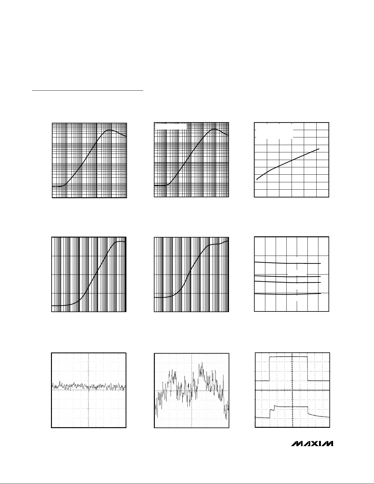
1.2470
1.2480
1.2475
1.2490
1.2485
1.2505
1.2500
1.2495
1.2510
-40 0-20 20 40 60 80 100
MAX6023EBT12
OUTPUT VOLTAGE
TEMPERATURE DRIFT
MAX6023 toc01
TEMPERATURE DRIFT (°C)
V
OUT
(V)
THREE
TYPICAL PARTS
4.986
4.990
4.988
4.996
4.994
4.992
5.002
5.000
4.998
5.004
-40 0 20-20 40 60 80 100
MAX6023EBT50
OUTPUT VOLTAGE
TEMPERATURE DRIFT
MAX6023 toc02
TEMPERATURE DRIFT (°C)
V
OUT
(V)
THREE
TYPICAL PARTS
4.993
4.995
4.994
4.999
4.998
4.997
4.996
5.002
5.001
5.000
5.003
0 300
400
500100 200 600 700 800 900 1000
MAX6023EBT50
LONG-TERM DRIFT
MAX6023 toc03
TIME (hr)
OUTPUT VOLTAGE (V)
THREE
TYPICAL PARTS
-100
0
200
100
300
400
264 8 10 12 14
MAX6023EBT12
LINE REGULATION
MAX6023 toc04
INPUT VOLTAGE (V)
OUTPUT VOLTAGE CHANGE (µV)
TA = +85°C
TA = -40°C
TA = +25°C
-200
0
400
200
600
800
5791113
MAX6023EBT50
LINE REGULATION
MAX6023 toc05
INPUT VOLTAGE (V)
OUTPUT VOLTAGE CHANGE (µV)
TA = +85°C
TA = -40°C
TA = +25°C
0
0.1
0.2
0.3
0.4
0.5
0.6
0.7
0.8
0 200 400 600 800 1000
MAX6023EBT25/30
DROPOUT VOLTAGE
vs. SOURCE CURRENT
MAX6023 toc06
SOURCE CURRENT (µA)
DROPOUT VOLTAGE (V)
TA = +85°C
TA = -40°C
TA = +25°C
-0.4
-0.2
0
0.2
0.4
-500 -250 0 250-375 -125 125 375 500
MAX6023EBT12
LOAD REGULATION
MAX6023 toc07
LOAD CURRENT (µA)
OUTPUT VOLTAGE CHANGE (mV)
TA = +85°C
TA = -40°C
TA = +25°C
-0.4
-0.2
0
0.2
0.4
-500 -250 0 250-375 -125 125 375 500
MAX6023EBT50
LOAD REGULATION
MAX6023 toc08
LOAD CURRENT (µA)
OUTPUT VOLTAGE CHANGE (mV)
TA = +85°C
TA = -40°C
TA = +25°C
0
0.10
0.05
0.20
0.15
0.25
0.30
0 400200 600 800 1000
MAX6023EBT41/45/50
DROPOUT VOLTAGE
vs. SOURCE CURRENT
MAX6023 toc09
SOURCE CURRENT (µA)
DROPOUT VOLTAGE (V)
TA = +85°C
TA = -40°C
TA = +25°C
Typical Operating Characteristics
(VIN= +5V for MAX6023EBT12/21/25/30/41/45, VIN= +5.5V for MAX6023EBT50; I
OUT
= 0; TA= +25°C, unless otherwise noted.) (Note 6)
Page 10
MAX6023
Precision, Low-Power, Low-Dropout, UCSP
Voltage Reference
10 ______________________________________________________________________________________
100 1k 10k 100k 1M 10M
MAX6023EBT12
POWER-SUPPLY REJECTION RATIO
vs. FREQUENCY
MAX6023 toc10
FREQUENCY (Hz)
PSRR (mV/V)
100
0.01
0.1
1
10
MAX6023EBT50
POWER-SUPPLY REJECTION RATIO
vs. FREQUENCY
MAX6023 toc11
FREQUENCY (Hz)
PSRR (mV/V)
100
0.01
0.1
1
10
10 10k 100k 1M100 1k 10M
VIN = +5.5V ±0.25V
20
26
24
22
28
30
32
34
36
38
40
264 8 10 12 14
SUPPLY CURRENT
vs. INPUT VOLTAGE
MAX6023 toc12
INPUT VOLTAGE (V)
SUPPLY CURRENT (µA)
VALID OVER SPECIFIED
V
IN
(MIN) TO VIN (MAX)
FOR EACH PART
0.01 100 10k10.1 10 1k 100k 1M
MAX6023EBT12
OUTPUT IMPEDANCE
vs. FREQUENCY
MAX6023 toc13
FREQUENCY (Hz)
OUTPUT IMPEDANCE (Ω)
0.1
1
10
100
1k
0.01 100 10k10.1 10 1k 100k 1M
MAX6023EBT50
OUTPUT IMPEDANCE
vs. FREQUENCY
MAX6023 toc14
FREQUENCY (Hz)
OUTPUT IMPEDANCE (Ω)
0.1
1
10
100
1k
20
25
30
35
40
SUPPLY CURRENT
vs. TEMPERATURE
MAX6023 toc15
TEMPERATURE (°C)
SUPPLY CURRENT (µA)
-40 20 40-20 0 60 80 100
VIN = 12.5V
VIN = 7.5V
VIN = 5.5V
VIN = 2.5V
Typical Operating Characteristics (continued)
(VIN= +5V for MAX6023EBT12/21/25/30/41/45, VIN= +5.5V for MAX6023EBT50; I
OUT
= 0; TA= +25°C, unless otherwise noted.) (Note 6)
V
OUT
10µV/div
1s/div
MAX6023EBT12
0.1Hz TO 10Hz OUTPUT NOISE
MAX6023 toc16
V
OUT
20µV/div
1s/div
MAX6023EBT50
0.1Hz TO 10Hz OUTPUT NOISE
MAX6023 toc17
V
IN
1V/div
V
OUT
1V/div
10µs/div
MAX6023EBT12
TURN-ON TRANSIENT
MAX6023 toc18
Page 11

MAX6023
Precision, Low-Power, Low-Dropout, UCSP
Voltage Reference
______________________________________________________________________________________ 11
I
OUT
40µA/div
V
OUT
20mV/div
10µs/div
MAX6023EBT12
LOAD-TRANSIENT RESPONSE
I
OUT
= ±25µA
MAX6023 toc19
I
OUT
50µA/div
V
OUT
50mV/div
20µs/div
MAX6023EBT50
LOAD-TRANSIENT RESPONSE
MAX6023 toc20
I
OUT
= ±25µA
V
IN
2V/div
V
OUT
2V/div
10µs/div
MAX6023EBT50
TURN-ON TRANSIENT
MAX6023 toc21
Typical Operating Characteristics (continued)
(VIN= +5V for MAX6023EBT12/21/25/30/41/45, VIN= +5.5V for MAX6023EBT50; I
OUT
= 0; TA= +25°C, unless otherwise noted.) (Note 6)
V
OUT
200V/div
I
OUT
1mA/div
10µs/div
MAX6023EBT12
LOAD-TRANSIENT RESPONSE
I
OUT
= ±500µA
MAX6023 toc22
I
OUT
500µA/div
V
OUT
200mV/div
20µs/div
MAX6023EBT50
LOAD-TRANSIENT RESPONSE
MAX6023 toc23
I
OUT
= ±500µA
V
IN
200mV/div
V
OUT
100mV/div
2µs/div
MAX6023EBT50
LINE-TRANSIENT RESPONSE
MAX6023 toc25
VIN = 5.5V ±0.25V
V
IN
200mV/div
V
OUT
100mV/div
2.5µs/div
MAX6023EBT12
LINE-TRANSIENT RESPONSE
MAX6023 toc24
VIN = 5V ±0.25V
Note 6: Many of the Typical Operating Characteristics of the MAX6023 family are extremely similar. The extremes of these characteristics
are found in MAX6023EBT12 (1.25V output) and the MAX6023EBT50 (5.0V output). The Typical Operating Characteristics of the
remainder of the MAX6023 family typically lie between these two extremes and can be estimated based on their output voltage.
Page 12
MAX6023
Precision, Low-Power, Low-Dropout, UCSP
Voltage Reference
12 ______________________________________________________________________________________
Detailed Description
The MAX6023 precision bandgap references use a
proprietary curvature correction circuit and lasertrimmed thin-film resistor, resulting in a low temperature
coefficient of <30ppm/°C and initial accuracy of better
than 0.2%. These devices can sink and source up to
500µA with <200mV of dropout voltage, making them
attractive for use in low-voltage applications.
Applications Information
Output/Load Capacitance
The MAX6023 devices do not require an output capacitor for dynamically stable, oscillation-free operation.
They are stable for capacitive loads from 0 to 2.2nF.
However, in applications where the load or the supply
can experience step changes, an output capacitor
reduces the amount of overshoot (or undershoot) and
improves the circuit’s transient response. Many applications do not need an external capacitor and this family offers a significant advantage in these applications
when board space is critical.
Supply Current
The no-load supply current of these series-mode references is 35µA maximum, and is virtually independent
of the supply voltage, with only a 0.8µA/V variation from
the supply voltage. Unlike shunt-mode references that
must draw the maximum load current at all times, the
load current is drawn from the input voltage source only
when required, so supply current is not wasted and efficiency is maximized at all input voltages. This improved
efficiency can help reduce power dissipation and
extend battery life.
When the supply voltage is below the minimum specified input voltage (as during turn-on), the devices can
draw up to 200µA beyond the nominal supply current.
The input voltage source must be capable of providing
this current to ensure reliable turn-on.
Output Voltage Hysteresis
Output voltage hysteresis is the change in the output
voltage at TA= +25°C before and after the device is
cycled over its entire operating temperature range.
Hysteresis is caused by differential package stress
appearing across the bandgap core transistors. The
typical temperature hysteresis value is 90ppm.
Turn-On Time
These devices typically turn on and settle within 0.1%
of their final value; 30µs to 220µs depending on the
device. The turn-on time can increase up to 1.5ms with
the device operating at the minimum dropout voltage
and the maximum load.
UCSP Information
UCSP Package Consideration
For general UCSP package information and PC layout
considerations, refer to the Maxim Application Note:
UCSP—A Wafer-Level Chip-Scale Package.
UCSP Reliability
The UCSP represents a unique package that greatly
reduces board space compared to other packages.
The chip-scale package represents a unique packaging form factor that may not perform as well as a packaged product through traditional mechanical reliability
tests. UCSP reliability is integrally linked to the user’s
assembly methods, circuit board material, and usage
environment. The user should closely review these
areas when considering use of a chip-scale package.
Performance through operating-life test and moisture
resistance remains uncompromised. The wafer-fabrication process primarily determines the performance.
Mechanical stress performance is a greater consideration for chip-scale packages. Chip-scale packages are
attached through direct solder contact to the user’s PC
board, foregoing the inherent stress relief of a packaged product lead frame. Solder joint contact integrity
must be considered. Comprehensive reliability tests
have been performed and are available upon request.
In conclusion, the UCSP performs reliably through environmental stresses.
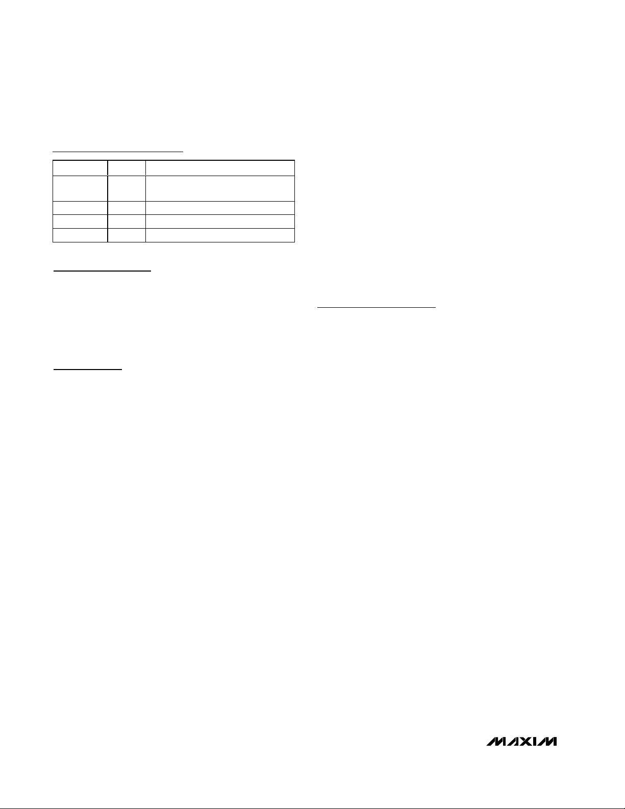
BUMP
FUNCTION
A1, A3 I.C.
Internally connected. Do not
connect to this pin.
A2
Ground
B1
Reference Output
B3 IN Input Voltage
Pin Description
NAME
GND
OUT
Page 13
Chip Information
TRANSISTOR COUNT: 70
MAX6023
Precision, Low-Power, Low-Dropout, UCSP
Voltage Reference
Maxim cannot assume responsibility for use of any circuitry other than circuitry entirely embodied in a Maxim product. No circuit patent licenses are
implied. Maxim reserves the right to change the circuitry and specifications without notice at any time.
Maxim Integrated Products, 120 San Gabriel Drive, Sunnyvale, CA 94086 408-737-7600 ____________________ 13
© 2002 Maxim Integrated Products Printed USA is a registered trademark of Maxim Integrated Products.
IN
I.C.
I.C.
GND
OUT
UCSP
B1
A1
B3 A3
A2
MAX6023
TOP VIEW
(BUMPS ON BOTTOM)
Pin Configuration
6L, UCSP.EPS
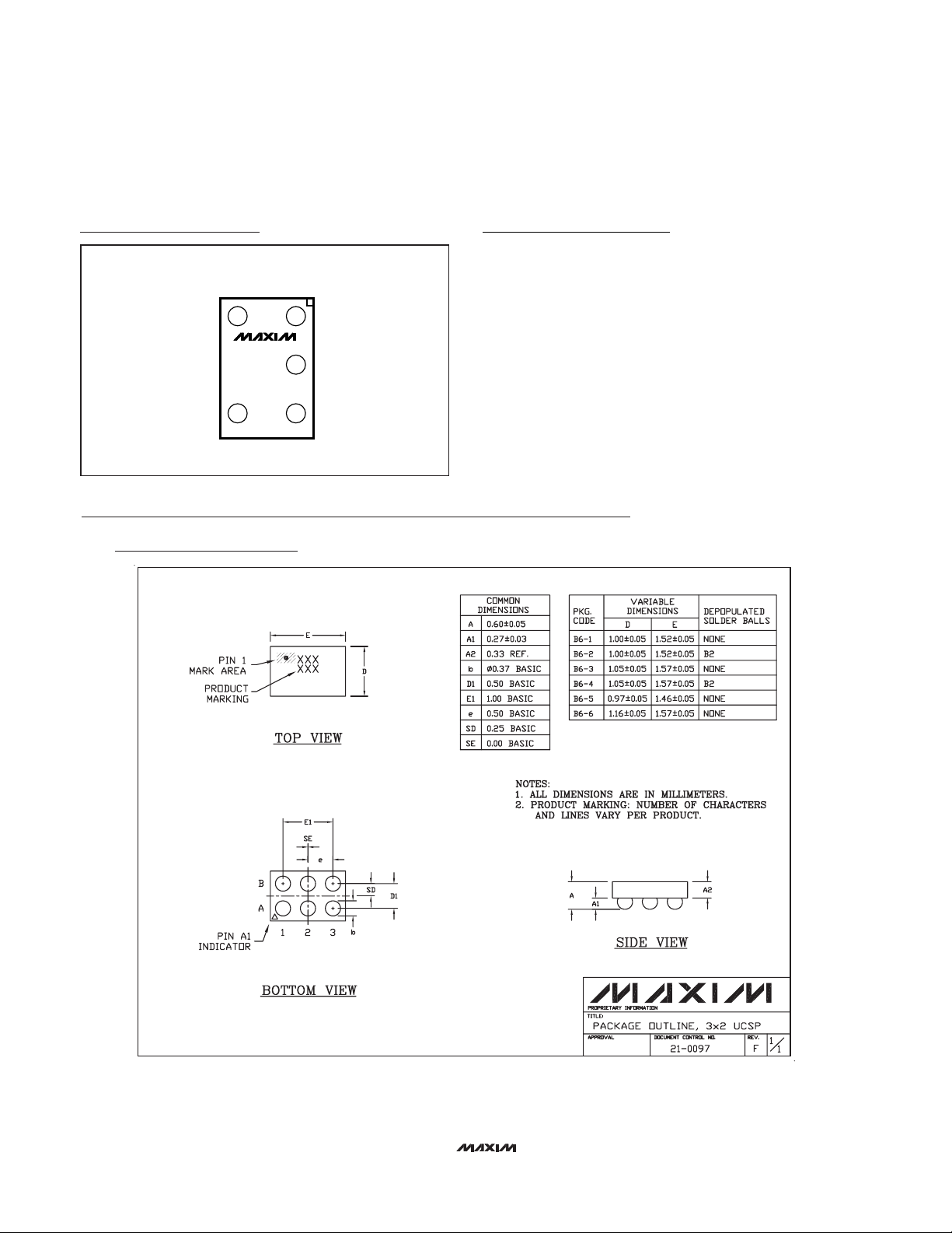
Package Information
(The package drawing(s) in this data sheet may not reflect the most current specifications. For the latest package outline information,
go to www.maxim-ic.com/packages
.
 Loading...