

General Description
The MAX6018 is a precision, low-voltage, low-dropout,
micropower voltage reference in a SOT23 package. This
three-terminal reference operates with an input voltage
from (V
OUT
+ 200mV) to 5.5V, and is available with out-
put voltage options of 1.2V, 1.6V, 1.8V, and 2.048V
The MAX6018 voltage reference consumes less than
5µA (max) of supply current and can source and sink
up to 1mA of load current. Unlike conventional shuntmode (two-terminal) references that waste supply current and require an external resistor, devices in the
MAX6018 family offer a supply current that is virtually
independent of supply voltage (with only 0.1µA/V variation with supply voltage) and do not require an external
resistor. The MAX6018 has initial accuracies of 0.2% (A
grade) and 0.4% (B grade) and temperature drift of
50ppm/°C (max). The low-dropout voltage and the
ultra-low, supply voltage-independent supply current
make this device ideal for two-cell alkaline, end-of-life,
battery-monitoring systems. The MAX6018 is available
in a tiny 3-pin SOT23 package.
Applications
Two-Cell, Battery-Operated Systems
Battery-Operated Equipment
Hand-Held Equipment
Data-Acquisition Systems
Industrial and Process-Control Systems
Features
♦ Ultra-Low Supply Current: 5µA (max)
♦ 1.6V Output from 1.8V Input
♦ Ultra-Small, 3-Pin SOT23 Package
♦ Initial Accuracy: ±0.2% (max)
♦ Low Temperature Drift: 50ppm/°C (max)
♦ 200mV Dropout Voltage
♦ Load Regulation (1mA Source): 700µV/mA (max)
♦ Line Regulation (V
OUT
+ 200mV) to 5.5V: 250µV/V
(max)
♦ Four Output Voltage Options: 1.2V, 1.6V,
1.8V, 2.048V
MAX6018
Precision, Micropower, 1.8V Supply,
Low-Dropout, SOT23 Voltage Reference
________________________________________________________________ Maxim Integrated Products 1
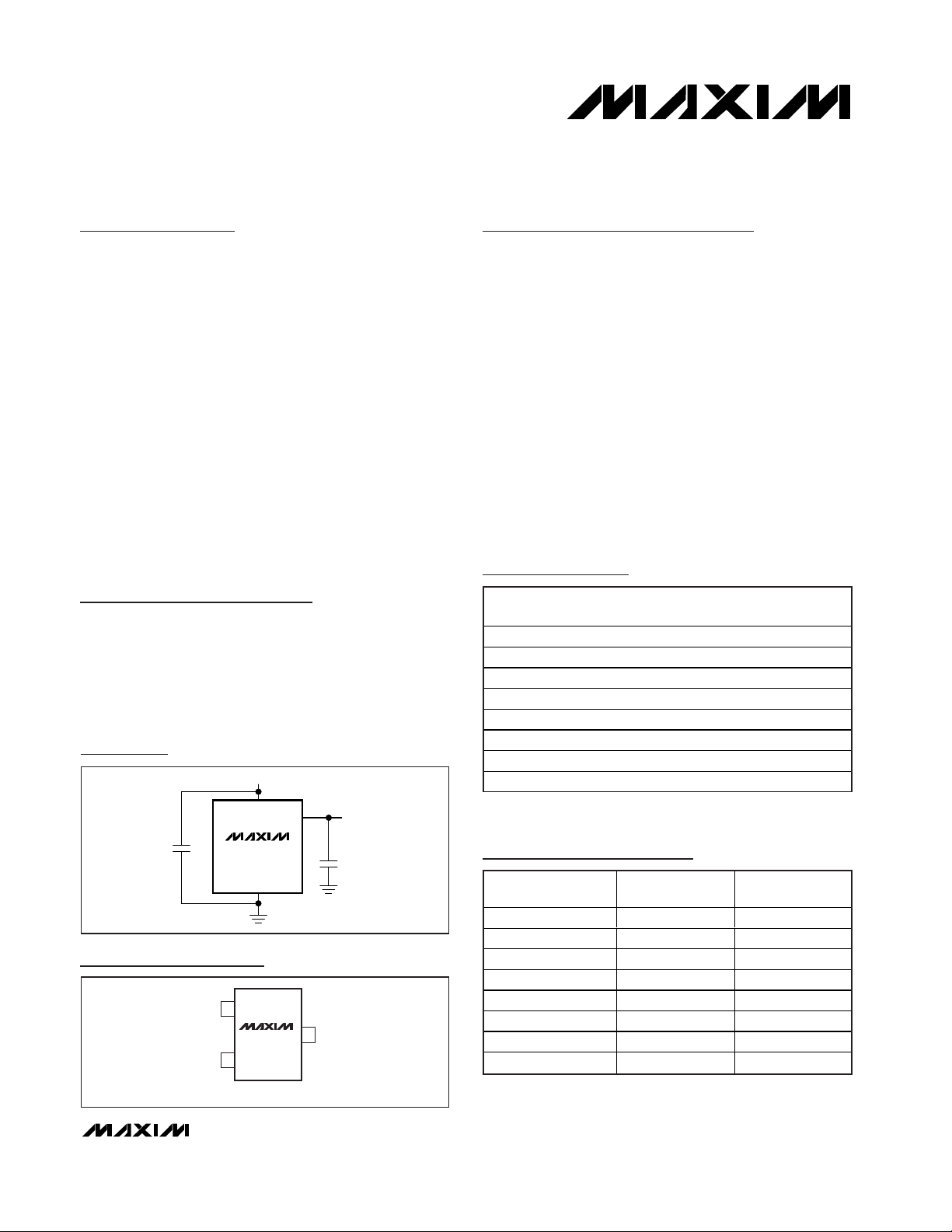
Ordering Information
*
IN
V
CC
OUT
REFERENCE
OUT
GND
MAX6018
*OPTIONAL
1µF, MAX*
Typical Application Circuit
19-2211; Rev 2; 12/02
For pricing, delivery, and ordering information, please contact Maxim/Dallas Direct! at
1-888-629-4642, or visit Maxim’s website at www.maxim-ic.com.
PART
PIN-
TOP
MARK
MAX6018AEUR12-T
FZJH
MAX6018BEUR12-T
FZJI
MAX6018AEUR16-T
FZJJ
MAX6018BEUR16-T
FZJK
MAX6018AEUR18-T
FZJL
MAX6018BEUR18-T
FZJM
MAX6018AEUR21-T
FZJN
MAX6018BEUR21-T
FZJO
Selector Guide
PART
OUTPUT
VOLTAGE (V)
INITIAL
ACCURACY (%)
MAX6018AEUR12 1.263 ±0.2
MAX6018BEUR12 1.263 ±0.4
MAX6018AEUR16 1.600 ±0.2
MAX6018BEUR16 1.600 ±0.4
MAX6018AEUR18 1.800 ±0.2
MAX6018BEUR18 1.800 ±0.4
MAX6018AEUR21 2.048 ±0.2
MAX6018BEUR21 2.048 ±0.4
Pin Configuration
TEMP RANGE
-40°C to +85°C 3 SOT23-3
-40°C to +85°C 3 SOT23-3
-40°C to +85°C 3 SOT23-3
-40°C to +85°C 3 SOT23-3
-40°C to +85°C 3 SOT23-3
-40°C to +85°C 3 SOT23-3
-40°C to +85°C 3 SOT23-3
-40°C to +85°C 3 SOT23-3
PACKAGE
TOP VIEW
1
IN
OUT
MAX6018
2
SOT23
3 GND
ABSOLUTE MAXIMUM RATINGS
Stresses beyond those listed under “Absolute Maximum Ratings” may cause permanent damage to the device. These are stress ratings only, and functional
operation of the device at these or any other conditions beyond those indicated in the operational sections of the specifications is not implied. Exposure to
absolute maximum rating conditions for extended periods may affect device reliability.
(Voltages Referenced to GND)
VIN............................................................................-0.3V to +6V
Output Short-Circuit Duration to GND or VIN............Continuous
Continuous Power Dissipation (TA= +70°C)
3-Pin SOT23 (derate 4.0mW/°C above +70°C).............320mW
Operating Temperature Range ...........................-40°C to +85°C
Junction Temperature......................................................+150°C
Storage Temperature Range .............................-65°C to +150°C
Lead Temperature (soldering, 10s) .................................+300°C
MAX6018
Precision, Micropower, 1.8V Supply,
Low-Dropout, SOT23 Voltage Reference
2 _______________________________________________________________________________________
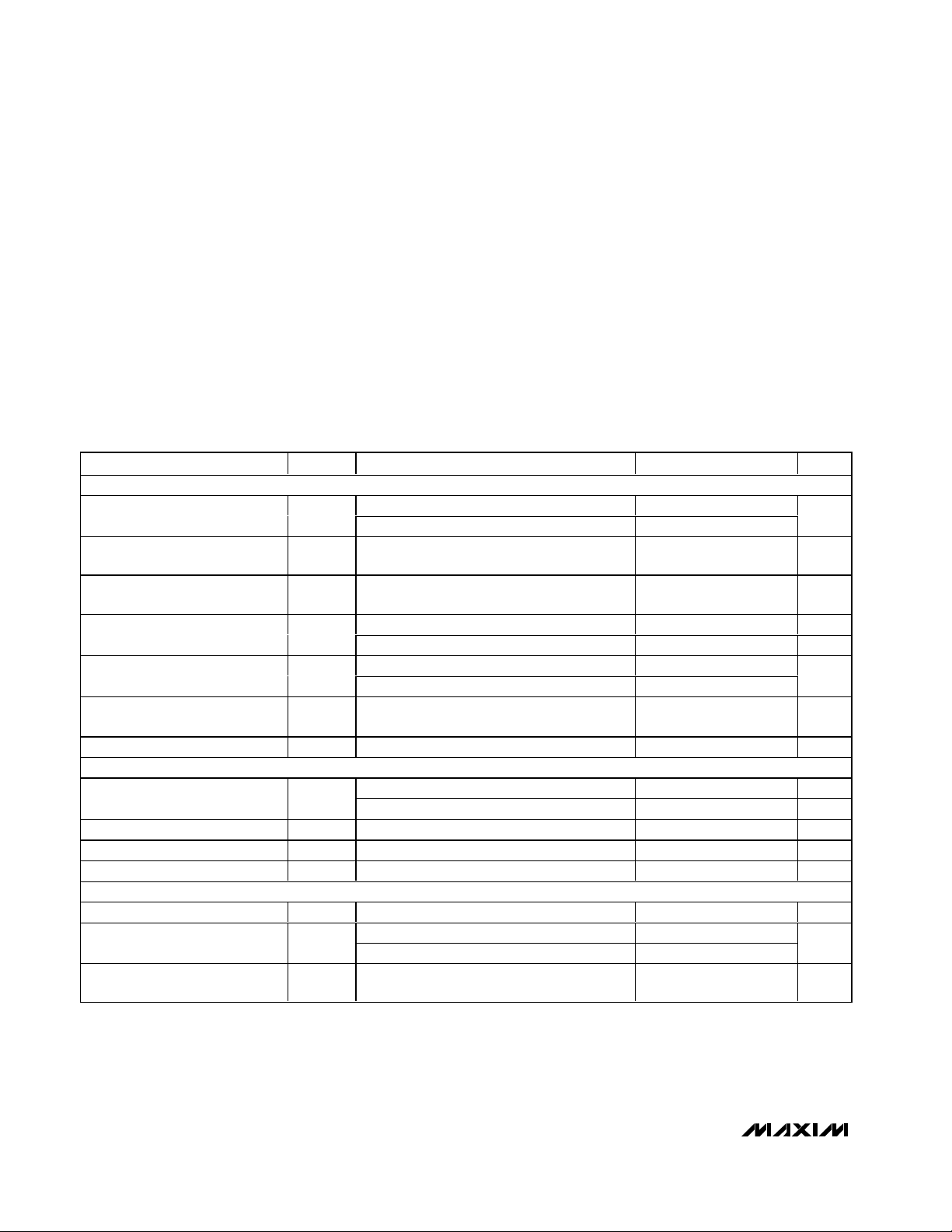
ELECTRICAL CHARACTERISTICS (MAX6018_12–1.263V)
(VIN= 1.8V; C
OUT
= 47nF, I
OUT
= 0; TA= T
MIN
to T
MAX
, unless otherwise noted. Typical values are at TA= +25°C.) (Note 1)
PARAMETER
CONDITIONS
UNITS
OUTPUT
MAX6018A_12 (0.2%)
Output Voltage V
OUT
MAX6018B_12 (0.4%)
V
Output Voltage Temperature
Drift
(Note 2) 16 50
ppm/oC
Line Regulation
∆V
IN
1.8V ≤ VIN ≤ 5.5V 50
µV/V
0 ≤ I
OUT
≤ 1mA 90
µV/mA
Load Regulation
∆I
OUT -100µA ≤ I
OUT
≤ 029
µV/µA
Sourcing to GND 3
Short-Circuit Current I
SC
Sinking from V
IN
6
mA
Long-Term Stability
Time
1000hrs at T
A
= +25°C
ppm
Thermal Hysteresis (Note 4)
ppm
DYNAMIC CHARACTERISTICS
0.1Hz to 10Hz 45
µVp-p
Noise Voltage e
OUT
10Hz to 10kHz
µV
RMS
Ripple Rejection VIN = 1.8V ±100mV (f = 120Hz) 85 dB
Turn-On Settling Time t
R
Settling to 0.1%; C
OUT
= 5nF
µs
Capacitive-Load Stability Range
C
OUT
(Note 2) 47
nF
INPUT
Supply Voltage Range V
IN
Guaranteed by Line Regulation Test
5.5 V
TA = +25°C35
Quiescent Supply Current I
IN
TA = T
MIN
to T
MAX
36
µA
Change in Quiescent Supply
Current vs. Input Voltage
1.8V ≤ VIN ≤ 5.5V 0.1 0.5
µA/V
SYMBOL
TCV
OUT
∆V
OUT
/
MIN TYP MAX
1.2605 1.2630 1.2655
1.2580 1.2630 1.2681
400
∆V
/
OUT
∆V
OUT
∆IIN/∆V
/
1.8
IN
100
130
100
200
700
1000
MAX6018
Precision, Micropower, 1.8V Supply,
Low-Dropout, SOT23 Voltage Reference
_______________________________________________________________________________________ 3
ELECTRICAL CHARACTERISTICS (MAX6018_16–1.600V)
(VIN= 1.8V; C
OUT
= 47nF, I
OUT
= 0; TA= T
MIN
to T
MAX
, unless otherwise noted. Typical values are at TA= +25°C.) (Note 1)
PARAMETER
CONDITIONS
UNITS
OUTPUT
MAX6018A_16 (0.2%) TA = +25°C
Output Voltage V
OUT
MAX6018B_16 (0.4%) TA = +25°C
V
Output Voltage Temperature
Drift
(Note 2) 16 50
ppm/oC
Line Regulation
∆V
IN
1.8V ≤ VIN ≤ 5.5V 40
µV/V
0 ≤ I
OUT
≤ 1mA 90
µV/mA
Load Regulation
∆I
OUT -750µA ≤ I
OUT
≤ 0 0.6 50
µV/µA
Dropout Voltage (Note 3)
I
OUT
= 1mA
200 mV
Sourcing to GND 6
Short-Circuit Current I
SC
Sinking from V
IN
2
mA
Long-Term Stability
Time
1000hrs at T
A
= +25°C
ppm
Thermal Hysteresis (Note 4)
ppm
DYNAMIC CHARACTERISTICS
0.1Hz to 10Hz 40
µVp-p
Noise Voltage e
OUT
10Hz to 10kHz
µV
RMS
Ripple Rejection VIN = 1.8V ±100mV (f = 120Hz) 85 dB
Turn-On Settling Time t
R
Settling to 0.1%; C
OUT
= 5nF
µs
Capacitive-Load Stability Range
C
OUT
(Note 2)
nF
INPUT
Supply Voltage Range V
IN
Guaranteed by Line Regulation Test
5.5 V
TA = +25°C35
Quiescent Supply Current I
IN
TA = T
MIN
to T
MAX
36
µA
Change in Quiescent Supply
Current vs. Input Voltage
1.8V ≤ VIN ≤ 5.5V 0.1 0.5
µA/V
SYMBOL
TCV
OUT
∆V
OUT
∆V
OUT
VIN - V
∆V
OUT
/
/
OUT
/
MIN TYP MAX
1.5968 1.6000 1.6032
1.5936 1.6000 1.6064
0.1 1000
1.8
250
700
100
100
130
150
200
∆IIN/∆V
IN

MAX6018
Precision, Micropower, 1.8V Supply,
Low-Dropout, SOT23 Voltage Reference
4 _______________________________________________________________________________________
ELECTRICAL CHARACTERISTICS (MAX6018_18–1.800V)
(VIN= 2.0V; C
OUT
= 47nF, I
OUT
= 0; TA= T
MIN
to T
MAX
, unless otherwise noted. Typical values are at TA= +25°C.) (Note 1)
PARAMETER
SYMBOL
CONDITIONS
MIN
TYP
MAX
UNITS
OUTPUT
MAX6018A_18 (0.2%) TA = +25°C
Output Voltage V
OUT
MAX6018B_18 (0.4%) TA = +25°C
V
Output Voltage Temperature Drift
(Note 2) 16 50
ppm/oC
Line Regulation
∆V
IN
2.0V ≤ VIN ≤ 5.5V 40
µV/V
0 ≤ I
OUT
≤ 1mA 90
µV/mA
Load Regulation
∆I
OUT -1mA ≤ I
OUT
≤ 0 0.4 50
µV/µA
Dropout Voltage (Note 3)
I
OUT
= 1mA
mV
Sourcing to GND 7.5
Short-Circuit Current I
SC
Sinking from V
IN
3
mA
Long-Term Stability
Time
1000hrs at T
A
= +25°C
ppm
Thermal Hysteresis (Note 4)
ppm
DYNAMIC CHARACTERISTICS
0.1Hz to 10Hz 45
µVp-p
Noise Voltage e
OUT
10Hz to 10kHz
µV
RMS
Ripple Rejection VIN = 2.0V ±100mV (f = 120Hz) 85 dB
Turn-On Settling Time t
R
Settling to 0.1%; C
OUT
= 5nF
µs
Capacitive-Load Stability Range
C
OUT
(Note 2)
nF
INPUT
Supply Voltage Range V
IN
Guaranteed by Line Regulation Test 2.0 5.5 V
TA = +25°C35
Quiescent Supply Current I
IN
TA = T
MIN
to T
MAX
36
µA
Change in Quiescent Supply
Current vs. Input Voltage
2V ≤ VIN ≤ 5.5V 0.1 0.5
µA/V
TCV
∆V
OUT
OUT
/
1.7964 1.8000 1.8036
1.7928 1.8000 1.8072
275
VIN - V
∆IIN/∆V
∆V
/
OUT
OUT
∆V
/
OUT
IN
100 200
100
130
160
200
0.1 1000
800

MAX6018
Precision, Micropower, 1.8V Supply,
Low-Dropout, SOT23 Voltage Reference
_______________________________________________________________________________________ 5
ELECTRICAL CHARACTERISTICS (MAX6018_21–2.048V)
(VIN= 2.25V; C
OUT
= 47nF, I
OUT
= 0; TA= T
MIN
to T
MAX
, unless otherwise noted. Typical values are at TA= +25°C.) (Note 1)
PARAMETER
CONDITIONS
UNITS
OUTPUT
MAX6018A_21 (0.2%) TA = +25°C
Output Voltage V
OUT
MAX6018B_21 (0.4%) TA = +25°C
V
Output Voltage Temperature Drift
(Note 2) 16 50
ppm/oC
Line Regulation
∆V
IN
2.25V ≤ VIN ≤ 5.5V 45
µV/V
0 ≤ I
OUT
≤ 1mA 90
µV/mA
Load Regulation
∆I
OUT -1mA ≤ I
OUT
≤ 0 0.3 50
µV/µA
Dropout Voltage (Note 3)
I
OUT
= 1mA
mV
Sourcing to GND 10
Short-Circuit Current I
SC
Sinking from V
IN
4
mA
Long-Term Stability
Time
1000hrs at T
A
= +25°C
ppm
Thermal Hysteresis (Note 4)
ppm
DYNAMIC CHARACTERISTICS
0.1Hz to 10Hz 50
µVp-p
Noise Voltage e
OUT
10Hz to 10kHz
µV
RMS
Ripple Rejection VIN = 2.25V ±100mV (f = 120Hz) 85 dB
Turn-On Settling Time t
R
Settling to 0.1%; C
OUT
= 5nF
µs
Capacitive-Load Stability Range
C
OUT
(Note 2)
nF
INPUT
Supply Voltage Range V
IN
Guaranteed by Line Regulation Test
5.5 V
TA = +25°C35
Quiescent Supply Current I
IN
TA = T
MIN
to T
MAX
36
µA
Change in Quiescent Supply
Current vs. Input Voltage
2.25V ≤ VIN ≤ 5.5V 0.1 0.5
µA/V
Note 1: Devices are 100% production tested at TA= +25°C and are guaranteed by design from TA= T
MIN
to T
MAX
.
Note 2: Not production tested. Guaranteed by design.
Note 3: Dropout voltage is the minimum input voltage at which V
OUT
changes ≤ 0.2% from V
OUT
at rated V
IN
and is guaranteed by
Load Regulation Test.
Note 4: Thermal hysteresis is defined as the change in T
A
= +25°C output voltage before and after temperature cycling of the device
(from T
A
= T
MIN
to T
MAX
). Initial measurement at TA= +25°C is followed by temperature cycling the device to TA= +85°C
then to T
A
= -40°C and another measurement at TA= +25°C is compared to the original measurement at TA= +25°C.
SYMBOL
MIN TYP MAX
2.0439 2.0480 2.0521
2.0398 2.0480 2.0562
TCV
OUT
∆V
/
OUT
∆V
/
OUT
VIN - V
∆V
OUT
OUT
/
100 200
100
130
175
200
0.1 1000
2.25
∆IIN/∆V
IN
330
1000

MAX6018
Precision, Micropower, 1.8V Supply,
Low-Dropout, SOT23 Voltage Reference
6 _______________________________________________________________________________________
Typical Operating Characteristics
(TA = +25°C, unless otherwise noted.)
1.2610
1.2615
1.2625
1.2620
1.2630
1.2635
-50 0-25 25 50 75 100
MAX6018_12
OUTPUT VOLTAGE DRIFT vs. TEMPERATURE
MAX6018 toc01
TEMPERATURE (°C)
OUTPUT VOLTAGE (V)
2.043
2.045
2.044
2.047
2.046
2.049
2.048
2.050
-50 0 25-25 50 75 100
MAX6018_21
OUTPUT VOLTAGE DRIFT vs. TEMPERATURE
MAX6018 toc02
TEMPERATURE (°C)
OUTPUT VOLTAGE (V)
1.260
1.263
1.262
1.261
1.264
1.265
1.266
0 400300100 200 500 600 700 800 900 1000
MAX6018_12
LONG-TERM DRIFT
MAX6018 toc03
TIME (HOURS)
OUTPUT VOLTAGE (V)
2.045
2.046
2.047
2.048
2.049
2.050
0 400 500200 300100 600 700 800 900 1000
MAX6018_21
LONG-TERM DRIFT
MAX6018 toc04
TIME (HOURS)
OUTPUT VOLTAGE (V)
0
0.05
0.15
0.10
0.20
0.25
1.5 2.5 3.02.0 3.5 4.0 4.5 5.0 5.5
MAX6018_12
LINE REGULATION
MAX6018 toc05
INPUT VOLTAGE (V)
OUTPUT VOLTAGE CHARGE (mV)
TA = +85°C
TA = -40°C
TA = +25°C
0
0.05
0.15
0.10
0.20
0.25
0.30
2.5 3.02.0 3.5 4.0 4.5 5.0 5.5
MAX6018_21
LINE REGULATION
MAX6018 toc06
INPUT VOLTAGE (V)
OUTPUT VOLTAGE CHANGE (mV)
TA = +25°C
TA = +85°C
TA = -40°C
0
20
40
60
80
100
120
140
0 0.40.2 0.6 0.8 1.0 1.2
MAX6018_21
DROPOUT VOLTAGE vs. SOURCE CURRENT
MAX6018 toc07
SOURCE CURRENT (mA)
DROPOUT VOLTAGE (mV)
TA = +85°C
TA = +25°C
TA = -40°C
-0.2
0
-0.1
0.2
0.1
0.4
0.3
0.5
0.7
0.6
0.8
-1.0 -0.6 -0.4 -0.2-0.8 0 0.2 0.4 0.80.6 1.0
MAX6018_12
LOAD REGULATION
MAX6018 toc08
LOAD CURRENT (mA)
OUTPUT VOLTAGE CHANGE (mV)
TA = +85°C
TA = -40°C
TA = +25°C
-0.2
0
-0.1
0.2
0.1
0.4
0.3
0.5
0.7
0.6
-1.0 -0.4 -0.2-0.6-0.8 0.40.20 0.6 0.8 1.0
MAX6018_21
LOAD REGULATION
MAX6018 toc09
SOURCE CURRENT (mA)
OUTPUT VOLTAGE CHANGE (mV)
TA = +85°C
TA = +25°C
TA = -40°C
6 _______________________________________________________________________________________
Typical Operating Characteristics
(TA = +25°C, unless otherwise noted.)

MAX6018
Precision, Micropower, 1.8V Supply,
Low-Dropout, SOT23 Voltage Reference
0
20
10
50
40
30
80
70
60
90
1 10010 1k 10k 100k
POWER-SUPPLY REJECTION RATIO
vs. FREQUENCY
MAX6018 toc10
FREQUENCY (Hz)
PSRR (dB)
2.90
3.05
3.00
2.95
3.10
3.15
3.20
3.25
3.30
3.35
3.40
132 456
SUPPLY CURRENT
vs. INPUT VOLTAGE
MAX6018 toc11
INPUT VOLTAGE (V)
SUPPLY CURRENT (µA)
MAX6018_12
MAX6018_16
MAX6018_18
MAX6018_21
0.01
1
0.1
10
100
1k
10k
100k
0.01 10.1 10 100 1k 10k
OUTPUT IMPEDANCE vs. FREQUENCY
MAX6018 toc12
FREQUENCY (Hz)
OUTPUT IMPEDANCE (Ω)
2.0
2.4
2.2
3.0
2.8
2.6
3.6
3.4
3.2
3.8
4.0
-50 0-25 25 50 75 100
SUPPLY CURRENT vs. TEMPERATURE
MAX6018 toc13
TEMPERATURE (°C)
SUPPLY CURRENT (µA)
VIN = 2.25V
VIN = 5.5V
VIN = 3V
20µV/div
MAX6018_21
0.1Hz TO 10Hz OUTPUT NOISE
MAX6018 toc14
10s/div
MAX6018_12
TURN-ON TRANSIENT
MAX6018 toc15
V
OUT
500mV/div
V
IN
1V/div
100µs/div
C
OUT
= 5nF
V
IN
1V/div
V
OUT
1V/div
MAX6018_21
TURN-ON TRANSIENT
MAX6018 toc16
50µs/div
C
OUT
= 5nF
V
IN
1V/div
V
OUT
1V/div
MAX6018_21
TURN-OFF TRANSIENT
MAX6018 toc17
2ms/div
C
OUT
= 5nF
MAX6018_12
LOAD-TRANSIENT RESPONSE
MAX6018 toc18
V
OUT
500mV/div
I
OUT
500µA/div
-300µA
+1mA
100µs/div
C
OUT
= 150pF
Typical Operating Characteristics (continued)
(TA = +25°C, unless otherwise noted.)
_______________________________________________________________________________________ 7

MAX6018
Precision, Micropower, 1.8V Supply,
Low-Dropout, SOT23 Voltage Reference
8 _______________________________________________________________________________________
Detailed Description
The MAX6018 is a precision, low-voltage, low-dropout,
micropower, bandgap voltage reference in a SOT23
package. This three-terminal reference operates with
an input voltage from (V
OUT
+ 200mV) to 5.5V, and is
available with output voltage options of 1.2V, 1.6V,
1.8V, and 2.048V. These devices can source up to 1mA
with <200mV of dropout voltage, making them attractive for use in low-voltage applications.
Applications Information
Output/Load Capacitance
These devices require a minimum of 100pF load to
maintain output stability.
They remain stable for capacitive loads as high as 1µF.
In applications where the load or the supply can experience step changes, a larger output capacitor reduces
the amount of overshoot (or undershoot) and assists
the circuit’s transient response. Otherwise, applications
may not need more than 100pF.
Supply Current
The 5µA maximum supply current varies only 0.1µA/V
with the supply voltage.
When the supply voltage is below the minimum-specified input voltage (as during turn-on), the devices can
draw up to 20µA beyond the nominal supply current.
The input voltage source must be capable of providing
this current to ensure reliable turn-on.
Turn-On Time
These devices typically turn on and settle to within
0.1% of their final value in 200µs. The turn-on time can
increase up to 1ms with the device operating at the
minimum dropout voltage and the maximum load.
Chip Information
TRANSISTOR COUNT: 87
PROCESS: BiCMOS
PIN
FUNCTION
1IN
Supply Voltage Input. Bypass with a 0.1µF
capacitor to ground.
2
Reference Voltage Output. Bypass with at
least 100pF to ground. (See Output/Load
Capacitance section).
3
Ground
Pin Description
I
OUT
1mA/div
+1mA
-1mA
V
OUT
1V/div
MAX6018_21
LOAD-TRANSIENT RESPONSE
MAX6018 toc19
100µs/div
C
OUT
= 150pF
MAX6018_12
LINE-TRANSIENT RESPONSE
MAX6018 toc20
V
OUT
50mV/div
V
IN
200mV/div
100µs/div
C
OUT
= 550pF
V
IN
200mV/div
V
OUT
50mV/div
MAX6018_21
LINE-TRANSIENT RESPONSE
MAX6018 toc21
100µs/div
C
OUT
= 550pF
Typical Operating Characteristics (continued)
(TA = +25°C, unless otherwise noted.)
NAME
OUT
GND

MAX6018
Precision, Micropower, 1.8V Supply,
Low-Dropout, SOT23 Voltage Reference
Maxim cannot assume responsibility for use of any circuitry other than circuitry entirely embodied in a Maxim product. No circuit patent licenses are
implied. Maxim reserves the right to change the circuitry and specifications without notice at any time.
Maxim Integrated Products, 120 San Gabriel Drive, Sunnyvale, CA 94086 408-737-7600 _____________________ 9
© 2002 Maxim Integrated Products Printed USA is a registered trademark of Maxim Integrated Products.
SOT23 L.EPS
Package Information
(The package drawing(s) in this data sheet may not reflect the most current specifications. For the latest package outline information,
go to www.maxim-ic.com/packages
.)
 Loading...