

General Description
The MAX6006–MAX6009 ultra-low-power shunt references are ideal for space-critical and low-power applications. They are offered in 3-pin SOT23 packages,
and the minimum operating current is guaranteed to be
<1µA. The devices feature low temperature coefficients
of <30ppm/°C and initial accuracy of better than 0.2%.
Available in +1.25V, +2.048V, +2.5V, and 3V output
voltages, the MAX6006–MAX6009 have references of
+1.25V, +2.048V, +2.5V, and +3.0V, respectively. The
devices can be used as lower-power, higher-precision
upgrades to the ICL8069, LM385, LT1004, and LM4040
references. The MAX6006–MAX6009 are available in
two grades: A and B. The A grade features a temperature coefficient of 30ppm/°C over the extended temperature range of -40°C to +85°C, with an initial accuracy
of 0.2%. Grade B features a temperature coefficient of
75ppm/°C with an initial accuracy of 0.5%. MAX6006
in+1.25V and MAX6008 in +2.5V are offered in 8-pin
SOIC packages, as plug in upgrades for LT1004 and
LM285.
________________________Applications
Battery-Powered Equipment
Portable Meters
Precision Regulators
A/D and D/A Converters
Features
♦ Ultra-Low Operating Current: Guaranteed <1µA
♦ Small 3-Pin SOT23 Package
♦ Initial Voltage Accuracy: 0.2%
♦ Temperature Coefficient: 30ppm/°C max
♦ Temperature Range: -40°C to +85°C
♦ Factory-Trimmed Output Voltages: +1.25V,
+2.048V, +2.5V, +3.0V
♦ Wide Operating Range: 1µA to 2mA
MAX6006–MAX6009
1µA SOT23 Precision Shunt
Voltage Reference
________________________________________________________________ Maxim Integrated Products 1
Pin Configuration
V
S
I
RMIN
+ I
L
I
L
I
RMIN
R
BIAS
V
OUT
V
R
MAX6006
MAX6007
MAX6008
MAX6009
0.01µF
R
BIAS
=
VS - V
R
IL + I
RMIN
Typical Operating Circuit
19-1730; Rev 0; 8/00
For free samples and the latest literature, visit www.maxim-ic.com or phone 1-800-998-8800.
For small orders, phone 1-800-835-8769.
Selector Guide
Ordering Information appears at end of data sheet
OUTPUT
PART
MAX6006A 1.25 0.2 30
MAX6006B 1.25 0.5 75
MAX6007A 2.048 0.2 30
MAX6007B 2.048 0.5 75
MAX6008A 2.5 0.2 30
MAX6008B 2.5 0.5 75
MAX6009A 3.0 0.2 30
MAX6009B 3.0 0.5 75
VOLTAGE
(V)
INITIAL
ACCURACY
(%)
TEMPERATURE
COEFFICIENT
(ppm/°C)
TOP VIEW
1
OUT
GND
2
SOT23-3
3 I.C.
MAX6006
MAX6007
MAX6008
MAX6009
N.C.
N.C.
1
2
3
4
SO
87OUT
N.C.N.C.
OUT
6
N.C.GND
5
MAX6006–MAX6009
1µA SOT23 Precision Shunt
Voltage Reference
2 _______________________________________________________________________________________
ABSOLUTE MAXIMUM RATINGS
ELECTRICAL CHARACTERISTICS—MAX6006
(TA= -40°C to +85°C, unless otherwise noted. Typical values are at TA= +25°C.) (Note 1)
Stresses beyond those listed under “Absolute Maximum Ratings” may cause permanent damage to the device. These are stress ratings only, and functional
operation of the device at these or any other conditions beyond those indicated in the operational sections of the specifications is not implied. Exposure to
absolute maximum rating conditions for extended periods may affect device reliability.
Operating Current (OUT to GND) ......................................20mA
Forward Current (GND to OUT) ..........................................20mA
Continuous Power Dissipation (T
A
= +70°C)
3-Pin SOT23 (derate 4mW/°C above +70°C)..............320mW
8-Pin SO (derate 5.48mW/°C above +70°C)...............471mW
Operating Temperature Range ...........................-40°C to +85°C
Storage Temperature Range .............................-65°C to +150°C
Lead Temperature (soldering, 10s) .................................+300°C
p-p
Reverse Breakdown Voltage V
Minimum Operating Current I
Reverse Breakdown Change
with Current
Reverse Dynamic Impedance IR = 1.2µA to 2mA (Note 2) 1.5 Ω
Low-Frequency Noise IR = 1.2µA, f = 0.1Hz to 10Hz 30 µV
Temperature Coefficient
(Note 3)
Long-Term Drift 1000h at TA = +25°C 150 ppm
Thermal Hysteresis (Note 4) 200 ppm
PARAMETER SYMBOL CONDITIONS MIN TYP MAX UNITS
TA = +25°C,
R
I
= 1.2µA
R
RMIN
TC I
VR change <0.2% from VR at IR = 1.2µA 0.5 1.0 µA
IR = 1.2µA to 200µA 1.0
= 200µA to 2mA 2.0
I
R
= 1.2µA
R
MAX6006A (0.2%) 1.2475 1.2500 1.2525
MAX6006B (0.5%) 1.2438 1.2500 1.2563
MAX6006A 30
MAX6006B 75
V
mV
ppm/°C
MAX6006–MAX6009
1µA SOT23 Precision Shunt
Voltage Reference
_______________________________________________________________________________________ 3
ELECTRICAL CHARACTERISTICS—MAX6007
(TA= -40°C to +85°C, unless otherwise noted. Typical values are at TA= +25°C.) (Note 1)
ELECTRICAL CHARACTERISTICS—MAX6008
(TA= -40°C to +85°C, unless otherwise noted. Typical values are at TA= +25°C.) (Note 1)
p-p
p-p
Reverse Breakdown Voltage V
Minimum Operating Current I
Reverse Breakdown Change
with Current
Reverse Dynamic Impedance IR = 1.2µA to 2mA (Note 2) 1.8 Ω
Low-Frequency Noise IR = 1.2µA, f = 0.1Hz to 10Hz 50 µV
Temperature Coefficient
(Note 3)
Long-Term Drift 1000h at TA = +25°C 150 ppm
Thermal Hysteresis (Note 4) 200 ppm
PARAMETER SYMBOL CONDITIONS MIN TYP MAX UNITS
R
RMIN
TC I
TA = +25°C,
I
= 1.2µA
R
VR change <0.2% from VR at IR = 1.2µA 0.5 1.0 µA
IR = 1.2µA to 200µA 1.3
I
= 200µA to 2mA 2.3
R
= 1.2µA
R
MAX6007A (0.2%) 2.0439 2.048 2.0521
MAX6007B (0.5%) 2.0378 2.048 2.0582
MAX6007A 30
MAX6007B 75
ppm/°C
Reverse Breakdown Voltage V
Minimum Operating Current I
Reverse Breakdown Change with
Current
Reverse Dynamic Impedance IR = 1.2µA to 2mA (Note 2) 2
Low-Frequency Noise IR = 1.2µA, f = 0.1Hz to 10Hz 60
Temperature Coefficient
(Note 3)
Long-Term Drift 1000h at TA = +25°C 150 ppm
Thermal Hysteresis (Note 4) 200 ppm
PARAMETER SYMBOL CONDITIONS MIN TYP MAX UNITS
R
RMIN
TC I
TA = +25°C,
I
= 1.2µA
R
VR change <0.2% from VR at IR = 1.2µA 0.5 1.0 µA
IR = 1.2µA to 200µA 1.5
= 200µA to 2mA 2.5
I
R
= 1.2µA
R
MAX6008A (0.2%) 2.4950 2.5000 2.5050
MAX6008B (0.5%) 2.4875 2.5000 2.5125
MAX6008A 30
MAX6008B 75
µ
ppm/°C
V
mV
V
mV
Ω
V

Typical Operating Characteristics
(CL = 0.01µF, TA = +25°C, unless otherwise noted.)
-3.0
-2.0
-2.5
-1.0
-1.5
0
-0.5
0.5
-50 0 50 100
TEMPERATURE DRIFT
MAX6006/9-01
TEMPERATURE (°C)
REFERENCE VOLTAGE CHANGE (mV)
IR = 1.2µA
V
OUT
= 2.5V
0.001 0.10.01 1 10
MAX6006
V
OUT
vs. CURRENT
MAX6006/9-02
REVERSE CURRENT (mA)
REVERSE VOLTAGE CHANGE (mV)
2.5
0
0.5
1.5
2.0
1.0
TA = +25°C
TA = +85°C
TA = -40°C
MAX6006
STARTUP
MAX6006/9-03
0
1.5V
1.2µA
20ms/div
MAX6006–MAX6009
1µA SOT23 Precision Shunt
Voltage Reference
4 _______________________________________________________________________________________
ELECTRICAL CHARACTERISTICS—MAX6009
(TA= -40°C to +85°C, unless otherwise noted. Typical values are at TA= +25°C.) (Note 1)
p-p
Note 1: All devices are 100% production tested at TA= +25°C and are guaranteed by design for TA= T
MIN
to T
MAX
, as specified.
Note 2: This parameter is guaranteed by the “reverse breakdown change with current” test.
Note 3: TC is measured by the “box” method; i.e., (V
MAX
- V
MIN
) / (T
MAX
- T
MIN
).
Note 4: Thermal hysteresis is defined as the change in the +25°C output voltage after cycling the device from T
MIN
to T
MAX
.
Reverse Breakdown Voltage V
Minimum Operating Current I
Reverse Breakdown Change
with Current
Reverse Dynamic Impedance IR = 1.2µA to 2mA (Note 2) 2.2 Ω
Low-Frequency Noise IR = 1.2µA, f = 0.1Hz to 10Hz 75 µV
Temperature Coefficient
(Note 3)
Long-Term Drift 1000h at TA = +25°C 150 ppm
Thermal Hysteresis (Note 4) 200 ppm
PARAMETER SYMBOL CONDITIONS MIN TYP MAX UNITS
R
RMIN
TA = +25°C,
I
= 1.2µA
R
VR change <0.2% from VR at IR = 1.2µA 0.5 1.0 µA
MAX6009A (0.2%) 2.9940 3.000 3.0060
MAX6009B (0.5%) 2.9850 3.000 3.0150
IR = 1.2µA to 200µA 1.7
= 200µA to 2mA 2.7
I
R
TC I
= 1.2µA
R
MAX6009A 30
MAX6009B 75
ppm/°C
V
mV

MAX6006–MAX6009
1µA SOT23 Precision Shunt
Voltage Reference
_______________________________________________________________________________________ 5
Typical Operating Characteristics (continued)
(CL = 0.01µF, TA = +25°C, unless otherwise noted.)
MAX6006
0.01Hz TO 10Hz NOISE
MAX6006/9-04
TIME (2s/div)
NOISE VOLTAGE (20µ/div)
1.2µA
1000
1
0.01 100 1000
MAX6006
OUTPUT IMPEDANCE vs. FREQUENCY
10
100
MAX6006/9-05
FREQUENCY (kHz)
IMPEDANCE (Ω)
0.1
10
1
IR = 6µA,
∆I
R
= 1.2µA
0.001 0.10.01 1 10
MAX6009
V
OUT
vs. CURRENT
MAX6006/9-06
REVERSE CURRENT (mA)
REVERSE VOLTAGE CHANGE (mV)
2.5
0
0.5
1.5
2.0
1.0
TA = +85°C
TA = +25°C
TA = -40°C
MAX6009
STARTUP
MAX6006/9-07
0
3V
20ms/div
1.2µA
1000
1
0.01 100 1000
MAX6009
OUTPUT IMPEDANCE vs. FREQUENCY
10
100
MAX6006/9-09
FREQUENCY (kHz)
IMPEDANCE (Ω)
0.1
10
1
IR = 6µA,
∆ I
R
= 1.2µA
MAX6009
0.01Hz TO 10Hz NOISE
MAX6006/9-08
NOISE VOLTAGE (20µV/div)
TIME (2s/div)

MAX6006–MAX6009
1µA SOT23 Precision Shunt
Voltage Reference
6 _______________________________________________________________________________________
Detailed Description
The MAX6006–MAX6009 are precision, two-terminal,
series bandgap voltage references. On-chip thin-film
resistors are laser trimmed to provide 0.2% output voltage accuracies. Voltages of +1.25V, +2.048V,+2.5V,
and +3.0V are available in the space-saving SOT23
package (2.1mm ✕2.7mm).
Applications Information
Output/Load Capacitance
For devices in this family, OUT needs to be bypassed
to GND with a 0.01µF or larger capacitor. In applications where the load or the supply can experience step
changes, additional capacitance will reduce the
amount of overshoot (or undershoot) and assist the circuit’s transient response.
Output Voltage Hysteresis
Output voltage hysteresis is the change in the output
voltage at T
A
= +25°C before and after the device is
cycled over its entire operating temperature range.
Hysteresis is caused by differential package stress
appearing across the bandgap core transistors. The
temperature hysteresis value is typically less than
200ppm.
Turn-On Time
The output capacitance and bias current of the
MAX6006–MAX6009 greatly affects turn-on settling
time. In the Typical Operating Characteristics, turn-on
time is shown with a 10nF output capacitor and a 1.2µA
bias current. Under these conditions, the MAX6006–
MAX6009 settle in 40ms. Settling time will linearly
decrease in proportion to the circuit’s bias current.
Typical Applications
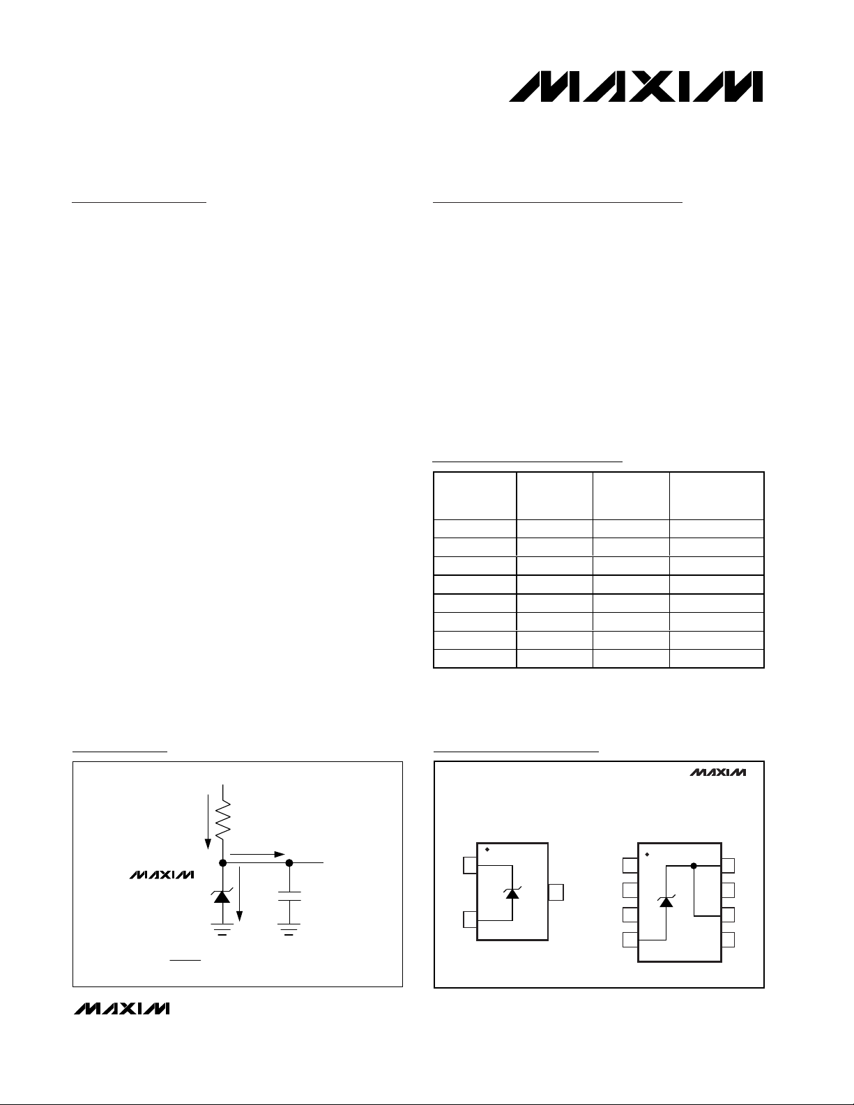
In the typical shunt regulator application shown in
Figure 1, R
BIAS
is used to set the current through the
load (IL) and the current through the shunt regulator
(I
RMIN
). There are two worst-case situations that R
BIAS
needs to be sized for:
1) R
BIAS
must be small enough that when VS(supply
voltage) is at its minimum and ILis at its maximum,
I
RMIN
is equal to at least the minimum operating
current of the shunt regulator.
2) R
BIAS
must be large enough that when VSis at its
maximum and ILis at its minimum, I
RMIN
is <2mA.
Pin Description
Figure 1. Typical Application Circuit
PIN NAME FUNCTION
SOT23 SO
1 6, 8 OUT
24
3 — IC Internally connected test point. Leave this pin unconnected, or connect to GND.
— 1, 2, 3, 5,7N.C. No connection. Not internally connected.
GND Ground
Output Voltage. Bias OUT with a pullup resistor to a potential greater than OUT. Bypass OUT
to GND with a 0.01µF or larger capacitor.
V
S
I
+ I
RMIN
L
R
BIAS
I
MAX6006
MAX6007
MAX6008
MAX6009
R
=
BIAS
IL + I
VS - V
RMIN
V
R
R
I
RMIN
L
V
OUT

MAX6006–MAX6009
1µA SOT23 Precision Shunt
Voltage Reference
_______________________________________________________________________________________ 7
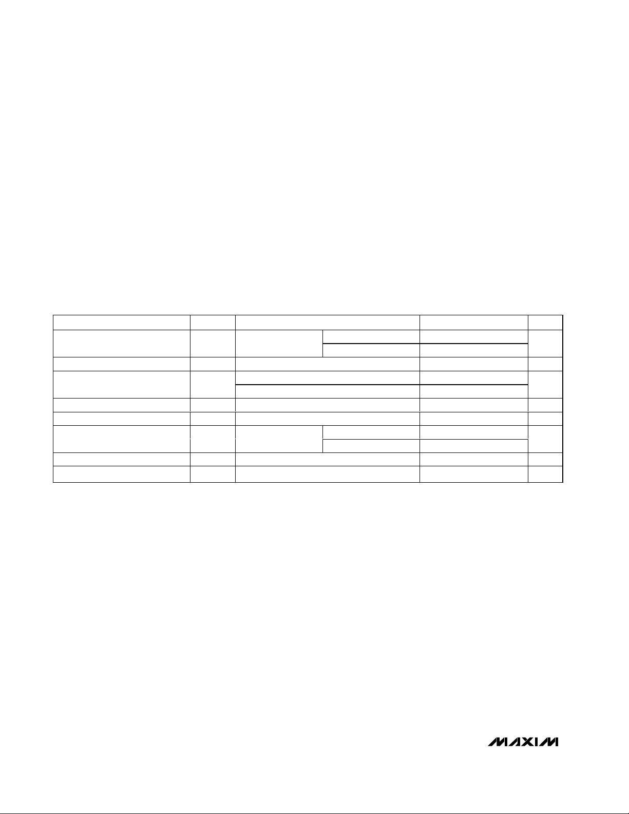
Figure 2. Precision 1µA to 1mA Current Sources
Ordering Information
Chip Information
TRANSISTOR COUNT: 60
PROCESS: BiCMOS
MAX6008 MAX6008
R1
200k
I
OUT
-1.0V TO -7V
PART
M A X6 0 0 6AE UR- T -40°C to +85°C 3 SOT23 FZGH
MAX6006AESA -40°C to +85°C 8 SO —
M AX 6006BE U R-T -40°C to +85°C 3 SOT23 FZGI
MAX6006BESA -40°C to +85°C 8 SO —
M A X6 0 0 7AE UR- T -40°C to +85°C 3 SOT23 FZGK
M AX 6007BE U R-T -40°C to +85°C 3 SOT23 FZGL
M A X6 0 0 8AE UR- T -40°C to +85°C 3 SOT23 FZGN
MAX6008AESA -40°C to +85°C 8 SO —
M AX6008BE U R- T -40°C to +85°C 3 SOT23 FZGO
MAX6008BESA -40°C to +85°C 8 SO —
M A X6 0 0 9AE UR- T -40°C to +85°C 3 SOT23 FZGQ
M AX6009BE U R- T -40°C to +85°C 3 SOT23 FZGR
2.5V
I
=
OUT
R2
TEMP.
RANGE
4
MAX4162EUK
3
-10V
PINPACKAGE
5
1
2
R2
TOP
MARK
R1
+1.0V TO +7V
200k
I
OUT
4
3
+10V
5
1
MAX4162EUK
2
R2

MAX6006–MAX6009
1µA SOT23 Precision Shunt
Voltage Reference
Maxim cannot assume responsibility for use of any circuitry other than circuitry entirely embodied in a Maxim product. No circuit patent licenses are
implied. Maxim reserves the right to change the circuitry and specifications without notice at any time.
8 _____________________Maxim Integrated Products, 120 San Gabriel Drive, Sunnyvale, CA 94086 408-737-7600
© 2000 Maxim Integrated Products Printed USA is a registered trademark of Maxim Integrated Products.
Package Information
SOTPO3L.EPS
 Loading...