
General Description
The MAX5957/MAX5958 triple hot-plug controllers are
designed for PCI Express (PCIe)
®
applications. These
devices provide hot-plug control for 12V, 3.3V, and 3.3V
auxiliary supplies of three PCIe slots. The MAX5957/
MAX5958s’ logic inputs/outputs allow interfacing directly
with the system hot-plug management controller or
through an SMBus™ with an external I/O expander such
as the MAX7313. An integrated debounced attention
switch and present-detect signals simplify system design.
The MAX5957/MAX5958 drive six external n-channel
MOSFETs to control the 12V and 3.3V main outputs. The
3.3V auxiliary outputs are controlled through 0.2Ω n-channel MOSFETs. Internal charge pumps provide the gate
drive for the 12V outputs while the gate drive of the 3.3V
output is driven by the 12V input supply clamped to 5.5V
above the respective 3.3V main supply rail. The 3.3V auxiliary outputs are completely independent from the main
outputs with their own charge pumps.
At power-up, the MAX5957/MAX5958 keep all the
MOSFETs (internal and external) off until the supplies rise
above their respective undervoltage lockout (UVLO)
thresholds. Upon a turn-on command, the MAX5957/
MAX5958 enhance the external and internal MOSFETs
slowly with a constant gate current to limit the power-supply inrush current.
The MAX5957/MAX5958 actively limit the current to protect all outputs at all times and shut down if an overcurrent condition occurs. After an overcurrent fault condition,
the MAX5957L/MAX5958L latch off while the MAX5957A/
MAX5958A automatically restart after a restart time delay.
The MAX5957/MAX5958 are offered in latch-off or autorestart versions (see the
Selector Guide
).
The MAX5957/MAX5958 are available in a 56-pin TQFN
package and operate over the -40°C to +85°C temperature range.
Applications
Servers
Desktop Mobile Server Platforms
Workstations
Embedded Devices
Features
o PCIe Compliant
o Hot Swap 12V, 3.3V, and 3.3V Auxiliary for 3
PCIe Slots
o Integrated Power MOSFETs for Auxiliary Supply
Rails
o Controls di/dt and dV/dt
o Active Current Limiting Protects Against
Overcurrent/Short-Circuit Conditions
o Programmable Current-Limit Timeout
o PWRGD Signal Outputs with Programmable
Power-On Reset (POR) (160ms Default)
o Latched FAULT Signal Output After Overcurrent
or Overtemperature Fault
o Attention Switch Inputs/Outputs with 4ms
Debounce
o Present-Detect Inputs
o Force-On Inputs Facilitate Testing/Debug
o Thermal Shutdown
o Allow Control Through SMBus with an I/O
Expander
MAX5957/MAX5958
Triple PCI Express, Hot-Plug Controllers
________________________________________________________________
Maxim Integrated Products
1
PART TEMP RANGE
PINPACKAGE
PKG
CODE
MAX5957AETN+ -40°C to +85°C 56 Thin QFN T5677-1
MAX5957LETN+ -40°C to +85°C 56 Thin QFN T5677-1
MAX5958AETN+ -40°C to +85°C 56 Thin QFN T5677-1
MAX5958LETN+ -40°C to +85°C 56 Thin QFN T5677-1
PART LATCH OFF AUTORESTART GUARANTEED AUX CURRENT (mA)
MAX5957AETN+ √ 375
MAX5957LETN+ √ 375
MAX5958AETN+ √ 550
MAX5958LETN+ √ 550
Selector Guide
Ordering Information
19-0884; Rev 0; 7/07
For pricing, delivery, and ordering information, please contact Maxim Direct at 1-888-629-4642,
or visit Maxim’s website at www.maxim-ic.com.
+
Denotes a lead-free package.
Pin Configuration and Typical Application Circuit appear at
end of data sheet.
PCI Express is a registered trademark of PCI-SIG Corp.
SMBus is a trademark of Intel Corp.

MAX5957/MAX5958
Triple PCI Express, Hot-Plug Controllers
2 _______________________________________________________________________________________
ABSOLUTE MAXIMUM RATINGS
ELECTRICAL CHARACTERISTICS
(V
12VIN
= V
12S_+
= V
12S_-
= 12V, V
3.3S_+=V3.3S_-
= V
3.3AUXIN
= V
ON_
= V
AUXON_
= V
FON_
= 3.3V, PWRGD_ = FAULT_ = PORADJ =
TIM = OUTPUT_ = 12G_ = 3.3G_ = OPEN, INPUT_ = PRES-DET_ = PGND = GND, T
A
= TJ= -40°C to +85°C, unless otherwise
noted. Typical values are at T
A
= TJ= +25°C.) (Note 1)
Stresses beyond those listed under “Absolute Maximum Ratings” may cause permanent damage to the device. These are stress ratings only, and functional
operation of the device at these or any other conditions beyond those indicated in the operational sections of the specifications is not implied. Exposure to
absolute maximum rating conditions for extended periods may affect device reliability.
(All voltages referenced to GND, unless otherwise noted.)
12VIN......................................................................-0.3V to +14V
12G_ ..........................................................-0.3V to (V
12VIN
+ 6V)
12S_+, 12S_-, 3.3G_ ..............................-0.3V to (V
12VIN
+ 0.3V)
3.3VAUXIN, ON_, FAULT_, PWRGD_.......................-0.3V to +6V
PGND ....................................................................-0.3V to +0.3V
All Other Pins ..................................-0.3V to (V
3.3VAUXIN
+ 0.3V)
Continuous Power Dissipation (T
A
= +70°C)
56-Pin Thin QFN (derate 40mW/°C above +70°C) .....3200mW
Operating Temperature Range ...........................-40°C to +85°C
Junction Temperature......................................................+150°C
Storage Temperature Range .............................-65°C to +150°C
Lead Temperature (soldering, 10s) .................................+300°C
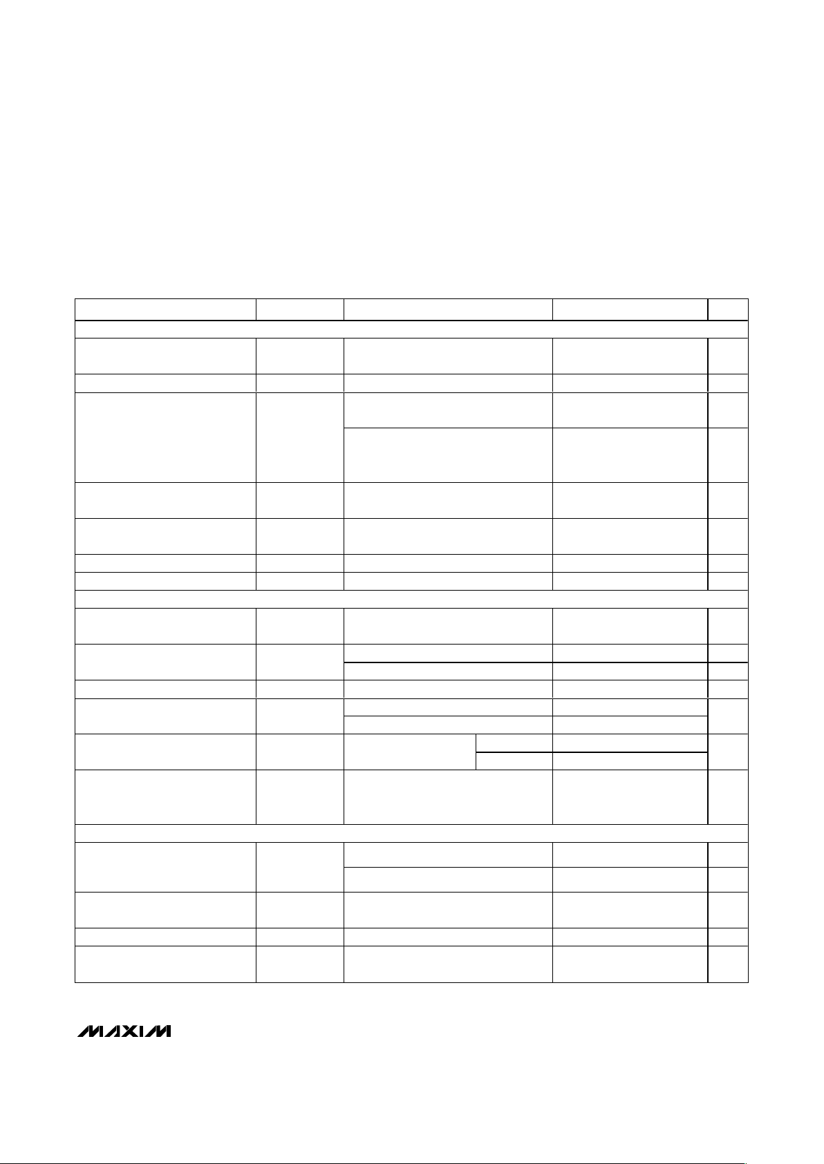
PARAMETER SYMBOL CONDITIONS MIN TYP MAX UNITS
12V SUPPLY (MAIN)
12V Supply Input-Voltage Range V
12VIN
10.8 12 13.2 V
V
12VIN
rising 9.5 10 10.5
12V Undervoltage Lockout V
12UVLO
Hysteresis 0.1
V
12V Undervoltage Lockout
Deglitch Time
t
DEG,UVLO
V
12IN
falling below V
12UVLO
to UVLO
assertion
30 µs
12V Supply Current I
12VIN
V
12VIN
= 13.2V 1 2.5 mA
12VIN CONTROL
12VIN Current-Limit Threshold
(V
12S+
- V
12S-
)
V
12ILIM
49 54 59 mV
12G_ Gate Charge Current I
12G, CHG
V
12G_
= GND 4 5 6 µA
Normal turn-off, ON_ = GND,
V
12G_
= 2V
50 150 250 µA
12G_ Gate Discharge Current I
12G_, DIS
Output short-circuit condition, strong
gate pulldown to regulation,
(V
12S+
- V
12S-)
≥ 1V, V
12G_
= 5V
60 120 200 mA
12G_ Gate High Voltage
(V
12G_
- V
12VIN
)
V
12G, H
I
12G
_ = 1µA 4.8 5.3 5.8 V
12G_ Threshold Voltage for
PWRGD_ Assertion
V
PGTH12
Referred to V
12VIN
, I
12G_
= 1µA
(Note 2)
3.0 4.0 4.8 V
12S_- Input Bias Current 1µA
12S_+ Input Bias Current 10 30 µA
3.3V SUPPLY (MAIN)
3.3V Supply Voltage Range V
3.3S_+
3.0 3.3 3.6 V
3.3SA+ rising 2.50 2.65 2.78 V
Undervoltage Lockout (Note 3)
Hysteresis 30 mV
MAX5957/MAX5958
Triple PCI Express, Hot-Plug Controllers
_______________________________________________________________________________________ 3
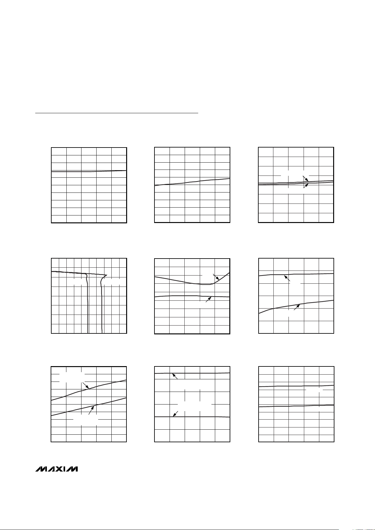
PARAMETER SYMBOL CONDITIONS MIN TYP MAX UNITS
3.3V CONTROL
3.3V Current-Limit Threshold
(V
3.3S_+
- V
3.3S_-
)
V
3.3ILIM
17 20 23 mV
3.3G_ Gate Charge Current I
3.3G_,CHG
V
3.3G_
= GND 4 5 6 µA
Normal turn-off, ON_ = GND,
V
3.3G
_ = 2V
50 150 250 µA
3.3G_ Gate Discharge Current I
3.3G_, DIS
Output short-circuit condition, strong
gate pulldown to regulation,
V
3.3S
_+ - V
3.3S_-
≥ 1V, V
3.3G-
= 5V
90 150 250 mA
3.3G_ Gate High Voltage
(V
3.3G_
- V
3.3S_+
)
V
3.3G_H
I
SOURCE
= 1µA 4.5 5.5 6.8 V
3.3G_ Threshold Voltage for
PWRGD_ Assertion
V
PGTH3.3
Referred to V
3.3AUXIN
, I
3.3G_
= 1µA
(Note 2)
3.0 4.0 4.5 V
3.3S_- Input Bias Current 1µA
3.3S_+ Input Bias Current 20 60 µA
3.3V AUXILIARY SUPPLY
3.3VAUXIN Supply Input Voltage
Range
V
3.3AUXIN
3.0 3.3 3.6 V
V
3.3VAUXIN
rising 2.50 2.65 2.78 V
3.3VAUXIN Undervoltage
Lockout
V
3.3VAUXUVLO
Hysteresis 30 mV
3.3VAUXIN Supply Current V
3.3VAUXIN
= 3.6V 2.5 5 mA
I
3.3VAUXO
= 375mA (MAX5957) 225
3.3VAUXIN to 3.3VAUXO
Maximum Dropout
I
3.3VAUXO
= 550mA (MAX5958) 280
mV
MAX5957 376 450 564
3.3VAUXO_ Current-Limit
Threshold
3.3VAUXO_ shorted
to GND
MAX5958 560 700 850
mA
3.3VAUXO_ Threshold for
PWRGD_ Assertion (V3.3VAUXIN
- V3.3VAUXO)
V
PGTH3.3AUX
(Note 2) 400 mV
LOGIC SIGNALS
Rising edge 1.0 2.0 V
Input-Logic Threshold (ON_,
FON_, AUXON_, PRES-DET_,
INPUT_)
Hysteresis 25 mV
Input Bias Current (ON_,
AUXON_, INPUT_)
1µA
FON_, PRES-DET_ Internal Pullup 25 50 75 kΩ
ON_, AUXON_ High-to-Low
Deglitch Time
4µs
ELECTRICAL CHARACTERISTICS (continued)
(V
12VIN
= V
12S_+
= V
12S_-
= 12V, V
3.3S_+=V3.3S_-
= V
3.3AUXIN
= V
ON_
= V
AUXON_
= V
FON_
= 3.3V, PWRGD_ = FAULT_ = PORADJ =
TIM = OUTPUT_ = 12G_ = 3.3G_ = OPEN, INPUT_ = PRES-DET_ = PGND = GND, T
A
= TJ= -40°C to +85°C, unless otherwise
noted. Typical values are at T
A
= TJ= +25°C.) (Note 1)

MAX5957/MAX5958
Triple PCI Express, Hot-Plug Controllers
4 _______________________________________________________________________________________
ELECTRICAL CHARACTERISTICS (continued)
(V
12VIN
= V
12S_+
= V
12S_-
= 12V, V
3.3S_+=V3.3S_-
= V
3.3AUXIN
= V
ON_
= V
AUXON_
= V
FON_
= 3.3V, PWRGD_ = FAULT_ = PORADJ =
TIM = OUTPUT_ = 12G_ = 3.3G_ = OPEN, INPUT_ = PRES-DET_ = PGND = GND, T
A
= TJ= -40°C to +85°C, unless otherwise
noted. Typical values are at T
A
= TJ= +25°C.) (Note 1)
PARAMETER SYMBOL CONDITIONS MIN TYP MAX UNITS
PRES-DET_ High-to-Low Deglitch
Time
t
DEG
357ms
V
PORADJ
= GND 1 µs
PORADJ = unconnected 90 160 250
R
PORADJ
= 20kΩ 35 55 75
R
PORADJ
= 100kΩ 145 265 380
PWRGD_ Power-On Reset
Deglitch Time (Note 2)
t
POR_HL
R
PORADJ
= 200kΩ 530
ms
PWRGD_ Low-to-High Deglitch
Time
t
POR_LH
4µs
I
SINK
= 2mA 0.1
PWRGD_, FAULT_ Output Low
Voltage
I
SINK
= 30mA 0.8
V
PWRGD_, FAULT_ Output High
Leakage Current
PWRGD_, FAULT_ = 5.5V 1 µA
TIM = open 5.5 11 17
R
TIM
= 15kΩ 1.4 2.6 3.8
R
TIM
= 120kΩ 12 22 32
FAULT_ Timeout t
FAULT
R
TIM
= 300kΩ 53
ms
FAULT_ Timeout During Startup t
SU
2 x
t
FAULT
ms
Autorestart Delay Time t
RESTART
64 x
t
FAULT
ms
Fault Reset Minimum Pulse Width t
RESET
(Note 4) 100 µs
Thermal Shutdown Threshold t
SD
TJ rising 150
Thermal Shutdown Hysteresis 20
°C
OUT_ Debounce Time t
DBC
2.6 4.4 6.2 ms
OUT_ Voltage High I
SOURCE
= 2mA
V
3.3 AU X IN
- 0.3
V
3.3 AU X IN
V
OUT_ Voltage Low I
SINK
= 2mA 0.4 V
Note 1: All devices are 100% production tested at TA= +25°C. Limits over temperature are guaranteed by design.
Note 2: PWRGD_ asserts a time t
POR_HL
after V
PGTH12,VPGTH3.3,
and V
PGTH3.3AUX
conditions are met.
Note 3: The UVLO for the 3.3V supply is sensed at 3.3S_+.
Note 4: This is the time that ON_ or AUXON_ must stay low when resetting a fault condition.
MAX5957/MAX5958
Triple PCI Express, Hot-Plug Controllers
_______________________________________________________________________________________
5
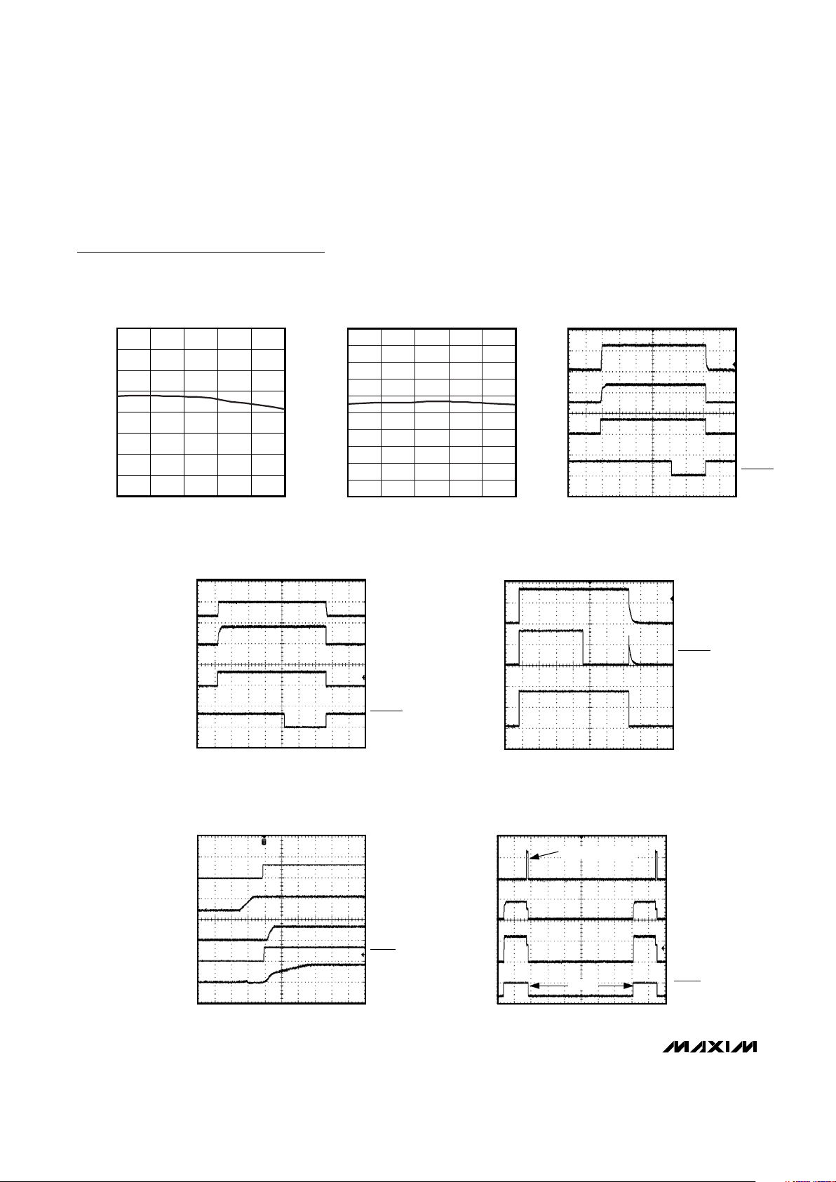
12V INPUT SUPPLY CURRENT
vs. TEMPERATURE
MAX5957 toc01
TEMPERATURE (°C)
SUPPLY CURRENT (mA)
603510-15
0.92
0.94
0.96
0.98
1.00
1.02
1.04
1.06
1.08
1.10
0.90
-40 85
3.3VAUXIN SUPPLY CURRENT
vs. TEMPERATURE
MAX5957 toc02
TEMPERATURE (°C)
3.3VAUXIN SUPPLY CURRENT (mA)
603510-15
0.5
1.0
1.5
2.0
2.5
3.0
3.5
4.0
4.5
5.0
0
-40 85
ON_ AND AUXON_ LOW-TO-HIGH THRESHOLD
VOLTAGE vs. TEMPERATURE
MAX5957 toc03
TEMPERATURE (°C)
THRESHOLD VOLTAGE (V)
603510-15
1.25
1.30
1.35
1.40
1.45
1.50
1.55
1.60
1.20
-40 85
ON_ THRESHOLD
AUXON_ THRESHOLD
3.3VAUXO_ OUTPUT VOLTAGE
vs. OUTPUT CURRENT
MAX5957 toc04
OUTPUT CURRENT (A)
OUTPUT VOLTAGE (V)
0.80.60.40.2 0.90.70.50.30.1
0.5
1.0
1.5
2.0
2.5
3.0
3.5
4.0
0
0 1.0
MAX5957 MAX5958
12G_ AND 3.3G_ GATE CHARGE
CURRENT vs. TEMPERATURE
MAX5957 toc05
TEMPERATURE (°C)
GATE CHARGE CURRENT (µA)
603510-15
4.80
4.85
4.90
4.95
5.00
5.05
5.10
5.15
5.20
4.75
-40 85
12G_
3.3G_
12G_ AND 3.3G_ GATE DISCHARGE
CURRENT vs. TEMPERATURE
MAX5957 toc06
TEMPERATURE (°C)
GATE DISCHARGE CURRENT (µA)
603510-15
160
165
170
175
180
150
155
-40 85
3.3G_
12G_
3.3VAUX INTERNAL SWITCH
MAXIMUM DROPOUT vs. TEMPERATURE
MAX5957 toc07
TEMPERATURE (°C)
DROPOUT VOLTAGE (V)
603510-15
0.02
0.04
0.06
0.08
0.10
0.12
0.14
0.16
0.18
0.20
0
-40 85
I
LOAD
= 550mA
MAX5958
I
LOAD
= 375mA
MAX5957
12V AND 3.3V CURRENT-LIMIT THRESHOLD
VOLTAGE vs. TEMPERATURE
MAX5957 toc08
TEMPERATURE (°C)
12V AND 3.3V CURRENT-LIMIT THRESHOLD (mV)
603510-15
10
20
30
40
50
60
0
-40 85
12V CURRENT-LIMIT
THRESHOLD
3.3V CURRENT-LIMIT
THRESHOLD
AUXILIARY CURRENT LIMIT
vs. TEMPERATURE
MAX5957 toc09
TEMPERATURE (°C)
AUXILIARY CURRENT (mA)
603510-15
0.10
0.30
0.20
0.40
0.50
0.60
0.70
0.80
0.90
1.00
0
-40 85
MAX5958
MAX5957
Typical Operating Characteristics
(V
12VIN
= V
12S_+
= 12V, V
3.3S_+
= V
3.3S_-
= V
3.3AUXIN
= V
ON_
= V
AUXON_
= V
FON_
= 3.3V, PWRGD_ = FAULT_ = PORADJ = TIM =
OUTPUT_ = OPEN, INPUT_ = PRES-DET_ = PGND = GND. See the
Typical Application Circuit
.)
MAX5957/MAX5958
Triple PCI Express, Hot-Plug Controllers
6 _______________________________________________________________________________________
Typical Operating Characteristics (continued)
(V
12VIN
= V
12S_+
= 12V, V
3.3S_+
= V
3.3S_-
= V
3.3AUXIN
= V
ON_
= V
AUXON_
= V
FON_
= 3.3V, PWRGD_ = FAULT_ = PORADJ = TIM =
OUTPUT_ = OPEN, INPUT_ = PRES-DET_ = PGND = GND. See the
Typical Application Circuit
.)
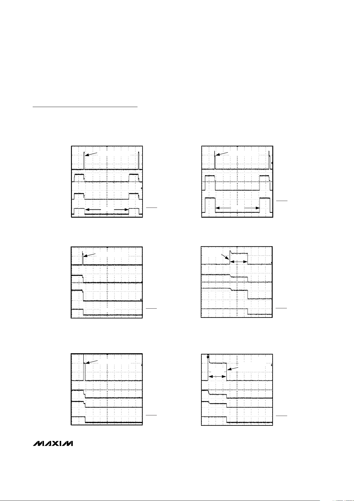
12V UNDERVOLTAGE LOCKOUT
THRESHOLD vs. TEMPERATURE
MAX5957 toc10
TEMPERATURE (°C)
UVLO THRESHOLD (V)
6035-15 10
9.85
9.90
9.95
10.00
10.05
10.10
10.15
10.20
9.80
-40 85
3.3VAUXON UNDERVOLTAGE LOCKOUT
THRESHOLD vs. TEMPERATURE
MAX5957 toc11
TEMPERATURE (°C)
UVLO THRESHOLD (V)
603510-15
2.54
2.58
2.62
2.66
2.70
2.52
2.56
2.60
2.64
2.68
2.50
-40 85
12V TURN-ON/TURN-OFF TIME
MAX5957 toc12
40ms/div
12V OUTPUT
VOLTAGE
12G_
ON_
PWRGD_
10V/div
20V/div
5V/div
5V/div
3.3V TURN-ON/TURN-OFF TIME
MAX5957 toc13
40ms/div
3.3V OUTPUT
5V/div
3.3G_
10V/div
ON_
5V/div
PWRGD_
5V/div
3.3V AUXILIARY TURN-ON/TURN-OFF TIME
MAX5957 toc14
40ms/div
3.3AUXO_OUTPUT
VOLTAGE
2V/div
AUXON_
2V/div
PWRGD_
2V/div
TURN-ON DELAY 3.3V OUTPUT AND
3.3V AUXILIARY OUTPUT
MAX5957 toc15
4ms/div
5V/div
5V/div
5V/div
5V/div
10V/div
3.3VAUXO_
OUTPUT VOLTAGE
3.3 OUTPUT VOLTAGE
3.3 INPUT,
3.3VAUXIN
3.3G_
PWRGD
FAULT CONDITION ON 12V MAIN OUTPUT
(AUTORESTART OPTION)
MAX5957 toc16
12G_
20V/div
0A
0V
0V
0V
FAULT_
5V/div
12V OUTPUT CURRENT
5A/div
100ms/div
12V OUTPUT VOLTAGE
10V/div
t
RESTART
R
LOAD
STEP TO 1.5Ω
MAX5957/MAX5958
Triple PCI Express, Hot-Plug Controllers
_______________________________________________________________________________________
7
Typical Operating Characteristics (continued)
(V
12VIN
= V
12S_+
= 12V, V
3.3S_+
= V
3.3S_-
= V
3.3AUXIN
= V
ON_
= V
AUXON_
= V
FON_
= 3.3V, PWRGD_ = FAULT_ = PORADJ = TIM =
OUTPUT_ = OPEN, INPUT_ = PRES-DET_ = PGND = GND. See the
Typical Application Circuit
.)
_______________________________________________________________________________________
7
FAULT CONDITION ON 3.3V MAIN OUTPUT
(AUTORESTART OPTION)
MAX5957 toc17
3.3G_
10V/div
FAULT_
5V/div
3.3V MAIN OUTPUT CURRENT
2A/div
100ms/div
3.3V OUTPUT VOLTAGE
5V/div
t
RESTART
R
LOAD
STEP TO 0.5Ω
0A
0V
0V
0V
FAULT CONDITION ON AUXILIARY OUTPUT
(AUTORESTART OPTION)
MAX5957 toc18
FAULT_
2V/div
3.3VAUXO_ OUTPUT CURRENT
500mA/div
100ms/div
3.3VAUXO_ OUTPUT VOLTAGE
2V/div
t
RESTART
R
LOAD
STEP TO 4Ω
0A
0V
0V
FAULT CONDITION ON 12V OUTPUT
(LATCH OPTION MAX5958)
MAX5957 toc19
12G_
20V/div
FAULT_
5V/div
12V OUTPUT CURRENT
5A/div
100ms/div
12V OUTPUT VOLTAGE
10V/div
R
LOAD
STEP TO 1.5Ω
FAULT CONDITION ON 12V OUTPUT
MAX5957 toc20
12G_
20V/div
FAULT_
5V/div
12V OUTPUT CURRENT
5A/div
4ms/div
12V OUTPUT VOLTAGE
10V/div
R
LOAD
STEP
TO 1.5Ω
t
FAULT
FAULT CONDITION ON 3.3V OUTPUT
(LATCHOFF OPTION)
MAX5957 toc21
3.3G_
10V/div
FAULT_
5V/div
3.3V OUTPUT CURRENT
2A/div
40ms/div
3.3V OUTPUT VOLTAGE
5V/div
R
LOAD
STEP TO 0.5Ω
FAULT CONDITION ON 3.3V MAIN OUTPUT
MAX5957 toc22
3.3G_
10V/div
FAULT_
5V/div
3.3V OUTPUT CURRENT
2A/div
4ms/div
3.3V OUTPUT VOLTAGE
5V/div
R
LOAD
STEP TO 0.5Ω
t
FAULT
MAX5957/MAX5958
Triple PCI Express, Hot-Plug Controllers
8 _______________________________________________________________________________________
Typical Operating Characteristics (continued)
(V
12VIN
= V
12S_+
= 12V, V
3.3S_+
= V
3.3S_-
= V
3.3AUXIN
= V
ON_
= V
AUXON_
= V
FON_
= 3.3V, PWRGD_ = FAULT_ = PORADJ = TIM =
OUTPUT_ = OPEN, INPUT_ = PRES-DET_ = PGND = GND. See the
Typical Application Circuit
.)
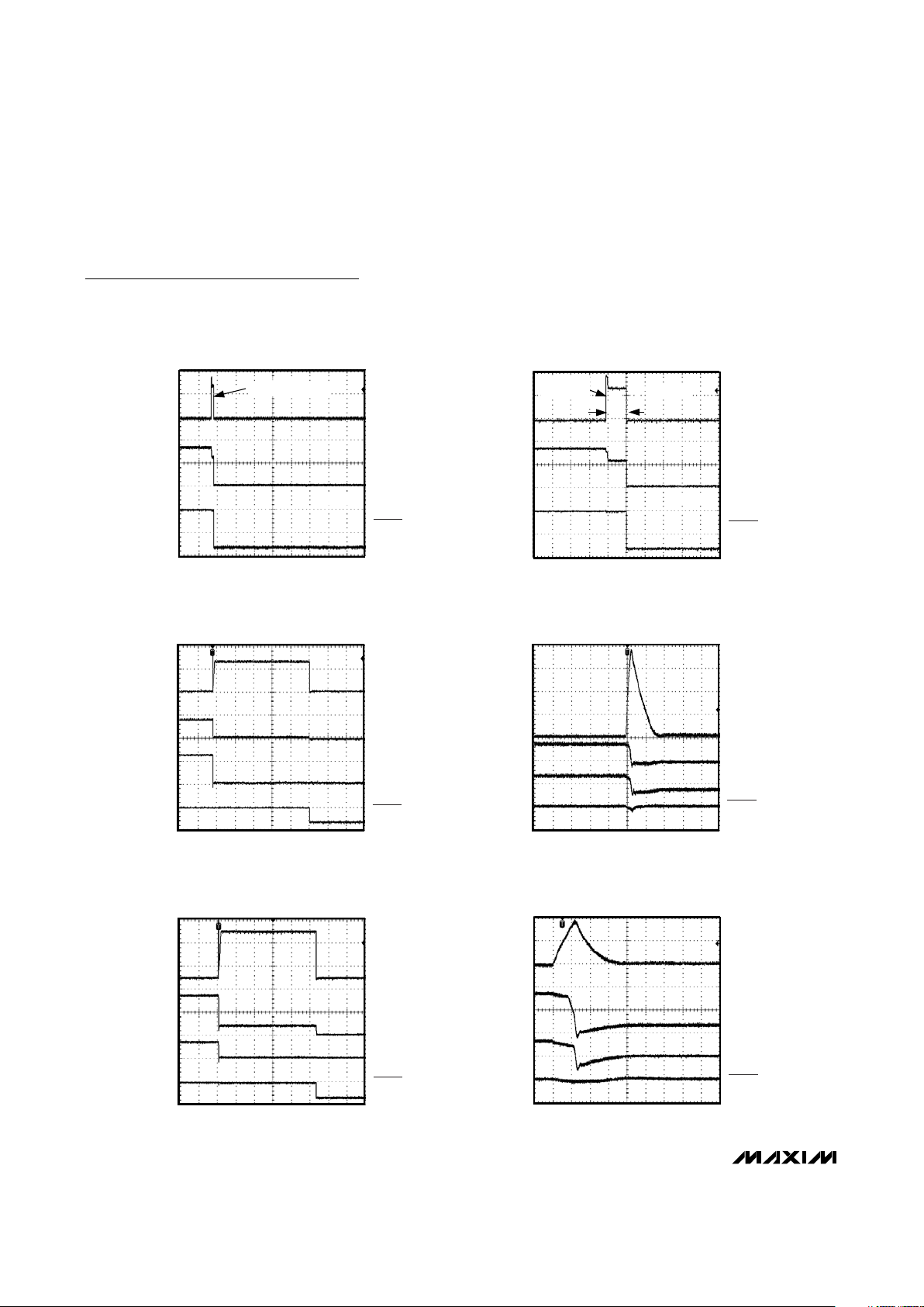
SHORT CIRCUIT ON 12V MAIN OUTPUT
MAX5957 toc25
12G_
20V/div
FAULT_
5V/div
12V OUTPUT CURRENT
5A/div
2ms/div
12V OUTPUT VOLTAGE
10V/div
SHORT CIRCUIT ON 12V MAIN OUTPUT
MAX5957 toc26
12G_
20V/div
FAULT_
5V/div
12V OUTPUT CURRENT
10A/div
4µs/div
12V OUTPUT VOLTAGE
10V/div
0V
0V
0V
FAULT CONDITION ON AUXILIARY OUTPUT
(LATCHOFF OPTION)
MAX5957 toc23
FAULT_
2V/div
3.3VAUXO_ OUTPUT CURRENT
500mA/div
100ms/div
3.3VAUXO_ OUTPUT VOLTAGE
2V/div
R
LOAD
STEP TO 3.5Ω
MAX5958
FAULT CONDITION ON AUXILIARY OUTPUT
MAX5957 toc24
FAULT_
2V/div
3.3VAUXO_ OUTPUT CURRENT
500mA/div
10ms/div
3.3VAUXO_ OUTPUT VOLTAGE
2V/div
R
LOAD
STEP TO 3Ω
t
FAULT
MAX5958
SHORT CIRCUIT ON 3.3V MAIN OUTPUT
MAX5957 toc27
3.3G_
5V/div
FAULT_
5V/div
3.3V OUTPUT CURRENT
2A/div
2ms/div
3.3V OUTPUT VOLTAGE
5V/div
SHORT CIRCUIT ON 3.3V MAIN OUTPUT
MAX5957 toc28
3.3G_
5V/div
FAULT_
5V/div
3.3V OUTPUT CURRENT
10A/div
2µs/div
3.3V OUTPUT VOLTAGE
5V/div
0V
 Loading...