

Page 1
General Description
The MAX5921/MAX5939 hot-swap controllers allow a circuit card to be safely hot plugged into a live backplane.
The MAX5921/MAX5939 operate from -20V to -80V and
are well suited for -48V power systems. These devices
are pin compatible with both the LT1640 and LT4250 and
provide improved features over these devices.
The MAX5921/MAX5939 provide a controlled turn-on to
circuit cards preventing damage to board connectors,
board components, and preventing glitches on the
power-supply rail. The MAX5921/MAX5939 provide
undervoltage, overvoltage, and overcurrent protection.
These devices ensure that the input voltage is stable
and within tolerance before applying power to the load.
Both the MAX5921 and MAX5939 protect a system
against overcurrent and short-circuit conditions by turning off the external MOSFET in the event of a fault condition. The MAX5921/MAX5939 protect against input
voltage steps by limiting the load current to a safe level
without turning off power to the load.
The device features an open-drain power-good status
output, PWRGD or PWRGD for enabling downstream
converters (see Selector Guide). A built-in thermal shutdown feature is also included to protect the external
MOSFET in case of overheating. The MAX5939 features
a latched fault output. The MAX5921 contains built-in
autoretry circuitry after a fault condition.
The MAX5921/MAX5939 are available in an 8-pin SO
package and operate in the extended -40°C to +85°C
temperature range.
Applications
Telecom Line Cards
Network Switches/Routers
Central-Office Line Cards
Server Line Cards
Base-Station Line Cards
Features
♦ Allows Safe Board Insertion and Removal
from a Live -48V Backplane
♦ Pin-Compatible with LT1640 and LT4250
♦ Circuit Breaker Immunity to Input Voltage Steps
and Current Spikes
♦ 450mA GATE Pulldown Current During Short-
Circuit Condition
♦ Exponential GATE Pulldown Current
♦ Withstands -100V Input Transients with No
External Components
♦ Programmable Inrush and Short-Circuit Current
Limits
♦ Operates from -20V to -80V
♦ Programmable Overvoltage Protection
♦ Programmable Undervoltage Lockout
with Built-In Glitch Filter
♦ Overcurrent Fault Integrator
♦ Powers Up into a Shorted Load
♦ Power-Good Control Output
♦ Thermal Shutdown Protects External MOSFET
MAX5921/MAX5939
-48V Hot-Swap Controllers with External
R
SENSE
and High Gate Pulldown Current
________________________________________________________________ Maxim Integrated Products 1
Pin Configuration
Ordering Information
19-2946; Rev 0; 9/03
For pricing, delivery, and ordering information, please contact Maxim/Dallas Direct! at
1-888-629-4642, or visit Maxim’s website at www.maxim-ic.com.
Typical Operating Circuit and Selector Guide appear at end
of data sheet.
Ordering Information continued at end of data sheet.
查询MAX5921供应商
PART TEMP RANGE PIN-PACKAGE
MAX5921AESA -40°C to +85°C 8 SO
MAX5921BESA -40°C to +85°C 8 SO
TOP VIEW
PWRGD
(PWRGD)
() FOR MAX5921B/F AND MAX5939B/F.
1
2
MAX5921
MAX5939
3
UV
4
EE
SO
87V
6
5
DD
DRAINOV
GATE
SENSEV
Page 2
MAX5921/MAX5939
-48V Hot-Swap Controllers with External
R
SENSE
and High Gate Pulldown Current
2 _______________________________________________________________________________________
ABSOLUTE MAXIMUM RATINGS
ELECTRICAL CHARACTERISTICS
(VEE= 0V, VDD= 48V, TA= -40°C to +85°C, unless otherwise noted. Typical values are at TA= +25°C, unless otherwise noted.) (Notes 1, 4)
Stresses beyond those listed under “Absolute Maximum Ratings” may cause permanent damage to the device. These are stress ratings only, and functional
operation of the device at these or any other conditions beyond those indicated in the operational sections of the specifications is not implied. Exposure to
absolute maximum rating conditions for extended periods may affect device reliability.
All Voltages Are Referenced to VEE, Unless Otherwise Noted
Supply Voltage (VDD- V
EE
)................................-0.3V to +100V
DRAIN, PWRGD, PWRGD ....................................-0.3V to +100V
PWRGD to DRAIN .............................................… -0.3V to +95V
PWRGD to VDD.......................................................-95V to +85V
SENSE (Internally Clamped) .................................-0.3V to +1.0V
GATE (Internally Clamped) ....................................-0.3V to +18V
UV and OV..............................................................-0.3V to +60V
Current into SENSE...........................................................+40mA
Current into GATE...........................................................+300mA
Current into Any Other Pin................................................+20mA
Continuous Power Dissipation (TA= +70°C)
8-Pin SO (derate 5.9mW/°C above +70°C)..................471mW
Operating Temperature Range ...........................-40°C to +85°C
Junction Temperature .....................................................+150°C
Storage Temperature Range .............................-65°C to +150°C
Lead Temperature (soldering, 10s) .................................+300°C
POWER SUPPLIES
Operating Input Voltage Range V
Supply Current I
GATE DRIVER AND CLAMPING CIRCUITS
Gate Pullup Current I
Gate Pulldown Current I
External Gate Drive ∆V
GATE to VEE Clamp Voltage V
CIRCUIT BREAKER
Current-Limit Trip Voltage V
SENSE Input Current I
UNDERVOLTAGE LOCKOUT
Supply Internal Undervoltage
Lockout Voltage High
Supply Internal Undervoltage
Lockout Voltage Low
UV INPUT
UV High Threshold V
UV Low Threshold V
UV Hysteresis V
UV Input Current I
OV INPUT
OV High Threshold V
OV Low Threshold V
OV Voltage Reference Hysteresis V
OV Input Current I
PARAMETER SYMBOL CONDITIONS MIN TYP MAX UNITS
DD
DD
PU
PD
GATEVGATE
GSCLMPVGATE
CL
SENSE
V
UVLOHVDD
V
UVLOLVDD
UVH
UVL
UVHY
INUV
OVH
OVL
OVHY
INOV
Current into VDD with UV = 3V, OV, DRAIN,
SENSE = V
GATE drive on, V
V
SENSE
VCL = V
V
SENSE
UV voltage increasing 1.240 1.255 1.270 V
UV voltage decreasing 1.105 1.125 1.145 V
UV = V
OV voltage rising 1.235 1.255 1.275 V
OV voltage decreasing 1.189 1.205 1.221 V
OV = V
, GATE = floating
EE
= V
GATE
- VEE = 100mV, V
- VEE, steady state, 20V ≤ VDD ≤ 80V 10 13.5 18 V
- VEE, IGS = 30mA 15 16.4 18 V
- V
SENSE
= 50mV -1 -0.2 0 µA
increasing 13.8 15.4 17.0 V
decreasing 11.8 13.4 15.0 V
EE
EE
EE
EE
= 2V (Note 2) 24 50 70 mA
GATE
20 80 V
0.7 2 mA
-30 -45 -60 µA
40 50 60 mV
130 mV
-0.5 0 µA
50 mV
-0.5 0 µA
Page 3
MAX5921/MAX5939
-48V Hot-Swap Controllers with External
R
SENSE
and High Gate Pulldown Current
_______________________________________________________________________________________ 3
ELECTRICAL CHARACTERISTICS (continued)
(VEE= 0V, VDD= 48V, TA= -40°C to +85°C, unless otherwise noted. Typical values are at TA= +25°C, unless otherwise noted.) (Notes 1, 4)
)
Note 1: All currents into device pins are positive; all currents out of device pins are negative. All voltages are referenced to VEE,
unless otherwise specified.
Note 2: Gate pulldown current after the current limit to GATE low (t
PHLCL
) time has elapsed.
Note 3: Minimum duration of GATE pulldown following a circuit breaker fault. The MAX5921_ automatically restarts after a circuit
breaker fault. The MAX5939_ is latched off and can be reset by toggling UV low. The GATE pulldown does not release until
t
OFF
has elapsed.
Note 4: The min/max limits are 100% production tested at +25°C and +85°C and guaranteed by design at -40°C.
PWRGD OUTPUT SIGNAL (REFERENCED TO DRAIN)
DRAIN Input Current I
DRAIN Threshold for PWRGD V
GATE High Threshold V
PWRGD, PWRGD Output
Leakage
PWRGD Low Voltage
(V
PWRGD Low Voltage
(V
OVERTEMPERATURE PROTECTION
Overtemperature Threshold T
Overtemperature Hysteresis T
AC PARAMETERS
OV High to GATE Low t
UV Low to GATE Low t
OV Low to GATE High t
UV High to GATE High t
SENSE High to GATE Low t
Current Limit to GATE Low t
DRAIN Low to PWRGD Low
DRAIN Low to (PWRGD - DRAIN)
High
GATE High to PWRGD Low
GATE High to (PWRGD - DRAIN)
High
TURN-OFF
Latch-Off Period t
PARAMETER SYMBOL CONDITIONS MIN TYP MAX UNITS
V
= 48V 10 80 250 µA
DRAIN
V
- VEE threshold for power-good
DRAIN
condition, DRAIN decreasing
∆V
- V
GATE
V
PWRGD
V
PWRGD
V
- V
DRAIN
(A, E versions)
V
= 5V, I
DRAIN
Junction temperature, temperature rising 135 °C
See Thermal Shutdown section 20 °C
Figures 1a, 2 0.5 µs
Figures 1a, 3 0.4 µs
Figures 1a, 2 3.3 µs
Figures 1a, 3 8.4 ms
Figures 1a, 4a 1 µs
Time from continuous
current limit to GATE
shutdown (see Overcurrent
Fault Integrator section),
Figures 1b, 4b
Figures 1a, 5a; A and E versions 8.2
Figures 1a, 5a; B and F versions 8.2
Figures 1a, 5b; A and E versions 8.2
Figures 1a, 5b; B and F versions 8.2
(Note 3) A, B, E, F versions
, decreasing 1.0 1.6 2.0 V
GATE
= 80V, V
= 80V, V
< VDL, I
EE
SINK
= 48V 10
DRAIN
= 0V 10
DRAIN
= 5mA
SINK
= 5mA (B, F versions) 0.11 0.4 V
A, B versions 0.35 0.5 0.65
E, F versions 1.4 2.0 2.6
1.1 1.7 2.0 V
0.11 0.4 V
128 x
t
PHLCL
PWRGD
PWRGD
- VEE)
- V
DRAIN
DRAIN
DL
GH
I
OH
V
OL
V
)
OL
OT(TH
HYS
PHLOV
PHLUV
PLHOV
PLHUV
PHLSENSE
PHLCL
t
PHLDL
t
PHLGH
OFF
µA
ms
ms
ms
ms
Page 4
MAX5921/MAX5939
-48V Hot-Swap Controllers with External
R
SENSE
and High Gate Pulldown Current
4 _______________________________________________________________________________________
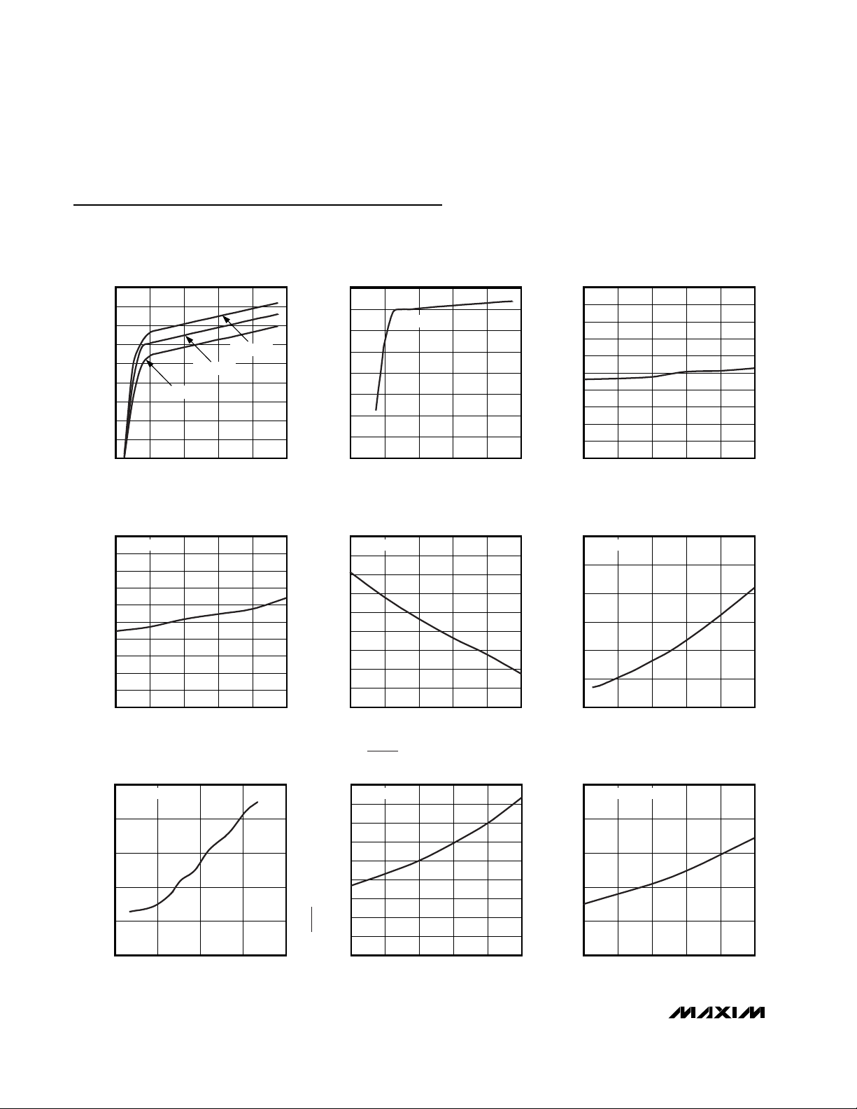
Typical Operating Characteristics
(VDD= +48V, VEE= 0V, TA = +25°C, unless otherwise noted.)
43.0
43.2
43.8
43.6
43.4
44.8
44.6
44.2
44.0
44.4
45.0
-40 10-15 356085
GATE PULLUP CURRENT
vs. TEMPERATURE
MAX5921TOC04
TEMPERATURE (°C)
GATE PULLUP CURRENT (µA)
V
GATE
= 0V
25
30
45
40
35
65
55
50
60
70
-40 10-15 356085
GATE PULLDOWN CURRENT
vs. TEMPERATURE AFTER A FAULT
MAX5921TOC05
TEMPERATURE (°C)
GATE PULLDOWN CURRENT (mA)
V
GATE
= 2V
0
15
60
45
30
75
90
04020 60 80 100
GATE PULLDOWN CURRENT
vs. OVERDRIVE DURING A CURRENT FAULT
MAX5921TOC06
OVERDRIVE (mV)
GATE PULLDOWN CURRENT (mA)
V
GATE
= 2V
0
100
400
300
200
500
600 900750 1050 1200
GATE PULLDOWN CURRENT
vs. OVERDRIVE DURING A SHORT CIRCUIT
MAX5921TOC07
OVERDRIVE (mV)
GATE PULLDOWN CURRENT (mV)
V
GATE
= 2V
0
40
160
120
80
20
140
100
60
180
-40 10-15 35 60 85
PWRGD OUTPUT LOW VOLTAGE
vs. TEMPERATURE (MAX5921A)
MAX5921TOC08
TEMPERATURE (°C)
PWRGD OUTPUT LOW VOLTAGE (mV)
I
OUT
= 5mA
0.001
0.01
10
1
0.1
100
-40 10-15 35 60 85
PWRGD OUTPUT LEAKAGE CURRENT
vs. TEMPERATURE (MAX5921B)
MAX5921TOC09
TEMPERATURE (°C)
PWRGD OUTPUT LEAKAGE CURRENT (nA)
V
DRAIN
- VEE > 2.4V
0
200
100
500
400
300
800
700
600
900
04020 60 80 100
SUPPLY CURRENT
vs. SUPPLY VOLTAGE
MAX5921TOC01
SUPPLY VOLTAGE (V)
SUPPLY CURRENT (µA)
TA = +85°C
TA = +25°C
TA = -40°C
7
9
8
12
11
10
14
13
15
04020 60 80 100
GATE VOLTAGE
vs. SUPPLY VOLTAGE
MAX5921TOC02
SUPPLY VOLTAGE (V)
GATE VOLTAGE (V)
TA = +25°C
40
42
48
46
44
58
56
52
50
54
60
-40 10-15 356085
CURRENT-LIMIT TRIP VOLTAGE
vs. TEMPERATURE
MAX5921TOC03
TEMPERATURE (°C)
TRIP VOLTAGE (mV)
Page 5
MAX5921/MAX5939
-48V Hot-Swap Controllers with External
R
SENSE
and High Gate Pulldown Current
_______________________________________________________________________________________ 5
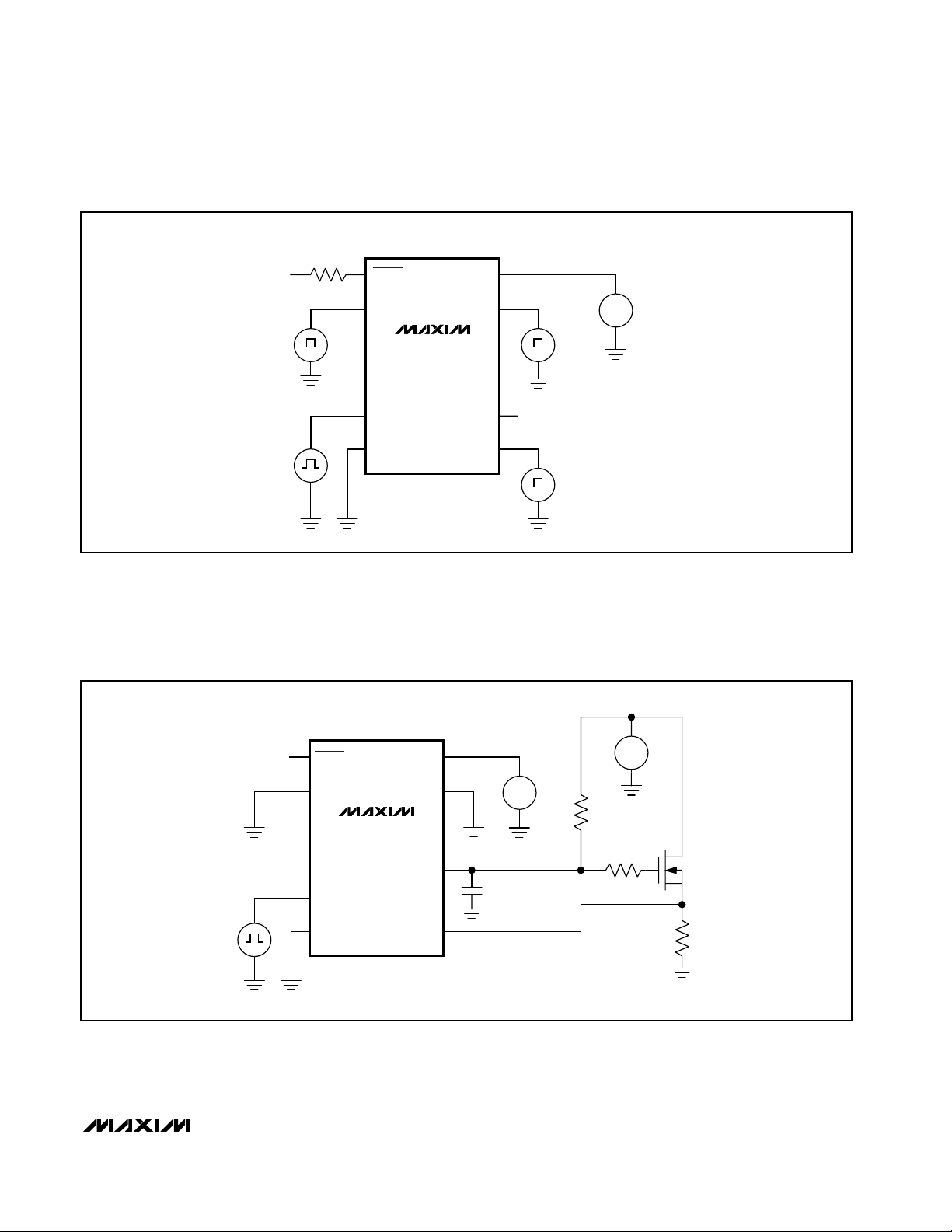
Figure 1a. Test Circuit 1
Figure 1b. Test Circuit 2
V+
5V
V
OV
V
UV
R
5kΩ
PWRGD/PWRGD
OV
MAX5921
MAX5939
UV
V
EE
V
DRAIN
GATE
SENSE
DD
+
V
+48V
S
-
V
DRAIN
V
SENSE
+
V
+20V
PWRGD/PWRGD
OV
V
DRAIN
DD
+
V
+48V
S
-
S
-
10kΩ
MAX5921
MAX5939
GATE
UV
V
V
UV
EE
SENSE
0.1µF
10Ω
IRF530
Page 6
MAX5921/MAX5939
-48V Hot-Swap Controllers with External
R
SENSE
and High Gate Pulldown Current
6 _______________________________________________________________________________________
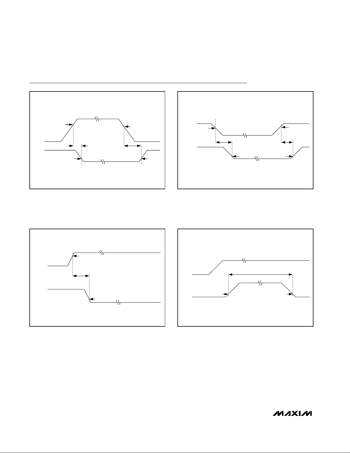
Timing Diagrams
Figure 2. OV to GATE Timing
Figure 3. UV to GATE Timing
Figure 4a. SENSE to GATE Timing
Figure 4b. Active Current-Limit Threshold
2V
1.255V
OV
0V
GATE
t
t
PHLOV
1V
PLHOV
1.205V
2V
1.125V
UV
0V
GATE
1V
t
PHLUV
1V
1.255V
t
PLHUV
1V
SENSE
GATE
100mV
V
EE
60mV
t
PHLSENSE
1V
UV
t
PHLCL
GATE
1V 1V
Page 7

MAX5921/MAX5939
-48V Hot-Swap Controllers with External
R
SENSE
and High Gate Pulldown Current
_______________________________________________________________________________________ 7
Timing Diagrams (continued)
Figure 5a. DRAIN to
PWRGD
/PWRGD Timing
Figure 5b. GATE to
PWRGD
/PWRGD Timing
Block Diagram
DRAIN
PWRGD
DRAIN
PWRGD
V
- V
= 0V
DRAIN
DCEN
1.4V
1.4V
t
PHLDL
1.4V
∆V
- V
= 0V
GATE
GATE
GATE
t
PHLGH
PWRGD
1.4V
∆V
- V
= 0V
GATE
GATE
GATE
PWRGD
- V
= 0V
DRAIN
1V
t
PHLGH
V
1V
t
PHLDL
V
EE
1V
V
EE
V
EE
1V
V
DCEN
V
EE
EE
V
DD
V
GATE
DRIVER
REF
DD
MAX5921/MAX5939
OUTPUT
DRIVER
V
DL
V
EE
V
GH
PWRGD
PWRGD
∆V
GATE
LOGIC
VDD AND
REFERENCE
GENERATOR
UV
REF
OV
50mV
V
SENSE GATE DRAIN
EE
UVLO
Page 8
MAX5921/MAX5939
-48V Hot-Swap Controllers with External
R
SENSE
and High Gate Pulldown Current
8 _______________________________________________________________________________________
Detailed Description
The MAX5921/MAX5939 integrated hot-swap controllers
for -48V power systems allow circuit boards to be safely
hot plugged into a live backplane without causing a
glitch on the power-supply rail. When circuit boards are
inserted into a live backplane, the bypass capacitors at
the input of the board’s power module or switching
power supply can draw large inrush currents as they
charge. Uncontrolled inrush currents can cause glitches
on the system power supply and damage components
on the board.
The MAX5921/MAX5939 provide a controlled turn-on to
circuit cards preventing damage to connectors, board
components, and prevent glitches on the power-supply
rail. Both the MAX5921/MAX5939 provide undervoltage, overvoltage, and overcurrent protection. The
MAX5921/MAX5939 ensure that the input voltage is stable and within tolerance before applying power to the
load. The device also provides protection against input
voltage steps by limiting the load current to a safe level
without turning off power to the load.
Pin Description
PIN
MAX5921A/
MAX5921E
MAX5939A/
MAX5939E
1 — PWRGD
— 1 PWRGD
22OV
33UV
44V
5 5 SENSE
6 6 GATE Gate Drive Output. Connect to the gate of the external N-channel MOSFET.
7 7 DRAIN
MAX5921B/
MAX5921F
MAX5939B/
MAX5939F
NAME FUNCTION
Power-Good Signal Output. PWRGD is an active-low open-drain status output referenced
to VEE. PWRGD latches low when V
power-good condition. PWRGD is open drain otherwise.
Power-Good Signal Output. PWRGD is an active-high open-drain status output referenced to DRAIN. PWRGD latches in a high-impedance state when V
and V
DRAIN otherwise.
Overvoltage Detection Input. OV is referenced to V
voltage, GATE pulls low. GATE remains low until the OV voltage reduces to V
V
OVHY
Undervoltage Detection Input. UV is referenced to V
voltage, the GATE is enabled. When UV is pulled below V
UV is also used to reset the circuit breaker after a fault condition. To reset the circuit
breaker, pull UV below V
condition; however, the device will not restart until a t
fault condition is removed.
Negative Power-Supply Input. Connect to the negative power-supply rail.
EE
Current-Sense Input. Connect to the external sense resistor and the source of the external
MOSFET. The voltage drop across the external sense resistor is monitored to detect
overcurrent or short-circuit fault conditions. Connect SENSE to V
limiting feature.
Output Voltage Sense Input. Connect to the output voltage node (drain of external Nchannel MOSFET). Place the MAX5921/MAX5939 such that DRAIN is close to the drain of
the external MOSFET for the best thermal protection.
GATE
.
> ∆V
- VEE ≤ VDL and V
DRAIN
- VGH indicating a power-good condition. PWRGD is pulled low to
GATE
. When OV is pulled above V
EE
. When UV is pulled above V
EE
. The reset command can be issued immediately after a fault
UVL
delay time has elapsed after the
OFF
> ∆V
GATE
DRAIN
, GATE pulls low.
UVL
to disable the current-
EE
GATE
indicating a
- VEE ≤ V
OVH
-
OVH
UVH
DL
88V
Positive Power-Supply Input. This is the power ground in the negative supply voltage
DD
system. Connect to the higher potential of the power-supply inputs.
Page 9

MAX5921/MAX5939
-48V Hot-Swap Controllers with External
R
SENSE
and High Gate Pulldown Current
_______________________________________________________________________________________ 9
Board Insertion
Figure 6a shows a typical hot-swap circuit for -48V systems. When the circuit board first makes contact with
the backplane, the DRAIN to GATE capacitance (Cgd)
of Q1 pulls up the GATE voltage to roughly IVEEx
(Cgd/C
gd
+ Cgs)I. The MAX5921/MAX5939 feature an
internal dynamic clamp between GATE and VEEto
keep the gate-to-source voltage of Q1 low during hot
insertion preventing Q1 from passing an uncontrolled
current to the load. For most applications, the internal
clamp between GATE and VEEof the MAX5921/
MAX5939 eliminates the need for an external gate-tosource capacitor. The resistor R3 limits the current into
the clamp circuitry during card insertion.
Power-Supply Ramping
The MAX5921/MAX5939 can reside either on the backplane or the removable circuit board (Figure 6a). Power
is delivered to the load by placing an external N-channel MOSFET pass transistor in the power-supply path.
After the circuit board is inserted into the backplane,
and the supply voltage at VEEis stable and within the
undervoltage and overvoltage tolerance, the
MAX5921/MAX5939 gradually turn on the external
MOSFET by charging the gate of Q1 with a 45µA current source. Capacitor C2 provides a feedback signal
to accurately limit the inrush current.
The inrush current can be calculated:
I
INRUSH
= I
PU
x CL / C2
where CLis the total load capacitance, C3 + C4, and
IPUis the gate pullup current.
Figure 6b shows the inrush current waveform. The current through C2 controls the GATE voltage. At the end
of the DRAIN ramp, the GATE voltage is charged to its
final value. The GATE-to-SENSE clamp limits the maximum ∆V
GATE
to 18V.
Board Removal
If the circuit card is removed from the backplane, the voltage at the UV falls below the UVLO detect threshold, and
the MAX5921/MAX5939 turn off the external MOSFET.
Current Limit and Electronic Circuit
Breaker
The MAX5921/MAX5939 provide current-limiting and circuit-breaker features that protect against excessive load
current and short-circuit conditions. The load current is
monitored by sensing the voltage across an external
sense resistor connected between VEEand SENSE.
Figure 6a. Inrush Control Circuitry/Typical Application Circuit
-48V RTN
SHORT PIN
-48V RTN
R4
549kΩ
1%
UV
R5
6.49kΩ
1%
OV
V
R6
10kΩ
1%
4.7nF
-48V
EE
SENSE GATE DRAIN
R1
0.02Ω
5%
V
DD
MAX5921
MAX5939
R2
10Ω
5%
Q1
IRF530
R3
1kΩ
5%
C2
15nF
100V
PWRGD
100µF
100V
GATE IN
+
V
IN
C4
0.1µF
100V
C3
V
IN
VICOR
VI-J3D-CY
-
Page 10

MAX5921/MAX5939
-48V Hot-Swap Controllers with External
R
SENSE
and High Gate Pulldown Current
10 ______________________________________________________________________________________
If the voltage between VEEand SENSE reaches the current-limit trip voltage (VCL), the MAX5921/MAX5939 pull
down the GATE and regulate the current through the
external MOSFET such that V
SENSE
- VEE< VCL. If the
current drawn by the load drops below V
CL
/ R
SENSE
limit, the GATE voltage rises again. However, if the load
current is at the regulation limit of V
CL
/ R
SENSE
for a peri-
od of t
PHLCL
, the electronic circuit breaker trips, causing
the MAX5921/MAX5939 to turn off the external MOSFET.
After an overcurrent fault condition, the MAX5921 automatically restarts after t
OFF
has elapsed. The MAX5939
circuit breaker is reset by toggling UV or by cycling
power. Unless power is cycled to the MAX5939, the
device waits until t
OFF
has elapsed before turning on the
gate of the external FET.
Load-Current Regulation
The MAX5921/MAX5939 accomplish load-current regulation by pulling current from GATE whenever V
SENSE
VEE> VCL. This decreases the gate-to-source voltage of
the external MOSFET, thereby reducing the load current.
When V
SENSE
- VEE< VCL, the MAX5921/MAX5939 pulls
GATE high by a 45µA (IPU) current.
Exponential Current Regulation
The MAX5921/MAX5939 provide an exponential pulldown current to turn off the external FET in response to
overcurrent conditions. The GATE pulldown current
increases (see Typical Operating Characteristics) in
response to V
SENSE
- VEEpotentials greater than 50mV
(VCL).
Load Current Regulation
(Short-Circuit Condition)
The MAX5921/MAX5939 devices also include a very
fast high-current pulldown source connected to GATE
(see Typical Operating Characteristics). The high-cur-
rent pulldown activates if V
SENSE
exceeds VEEby
650mV (typ) during a catastrophic overcurrent or shortcircuit fault condition. The high-current pulldown circuit
sinks as much as 450mA from GATE to turn off the
external MOSFET.
Immunity to Input Voltage Steps
The MAX5921/MAX5939 guard against input voltage
steps on the input supply. A rapid increase in the input
supply voltage (VDD- VEEincreasing) causes a current
step equal to I = CL x ∆V
IN
/ ∆t, proportional to the input
voltage slew rate (∆V
IN
/ ∆t). If the load current exceeds
V
CL
/ R
SENSE
during an input voltage step, the MAX5921/
MAX5939 current limit activates, pulling down the gate
voltage and limiting the load current to V
CL
/ R
SENSE
. The
DRAIN voltage (V
DRAIN
) then slews at a slower rate than
the input voltage. As the drain voltage starts to slew
down, the drain-to-gate feedback capacitor C2 pushes
back on the gate, reducing the gate-to-source voltage
(VGS) and the current through the external MOSFET.
Once the input supply reaches its final value, the DRAIN
slew rate (and therefore the inrush current) is limited by
the capacitor C2 just as it is limited in the startup condition (see the Power-Supply Ramping section). To ensure
correct operation, R
SENSE
must be chosen to provide a
current limit larger than the sum of the load current and
the dynamic current into the load capacitance in the
slewing mode.
If the load current plus the capacitive charging current is
below the current limit, the circuit breaker does not trip.
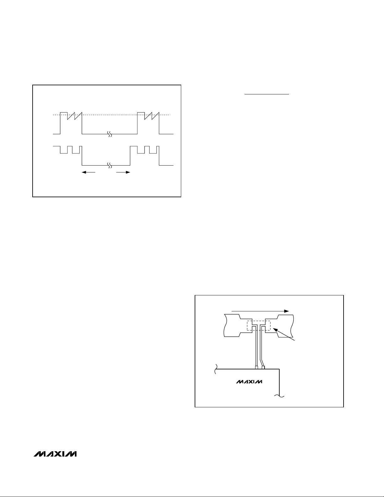
Undervoltage and Overvoltage Protection
Use UV and OV to detect undervoltage and overvoltage
conditions. UV and OV internally connect to analog comparators with 130mV (UV) and 50mV (OV) of hysteresis.
When the UV voltage falls below its threshold or the OV
voltage rises above its threshold, GATE pulls low. GATE
is held low until UV goes high and OV is low, indicating
that the input supply voltage is within specification. The
MAX5921/MAX5939 includes an internal lockout (UVLO)
that keeps the external MOSFET off until the input supply
voltage exceeds 15.4V, regardless of the UV input.
UV is also used to reset the circuit breaker after a fault
condition has occurred. Pull UV below V
UVL
to reset the
circuit breaker.
Figure 6b. Inrush Control Waveforms
INRUSH
CURRENT
1A/div
GATE - V
EE
10V/div
DRAIN
50V/div
V
EE
50V/div
4ms/div
Page 11

MAX5921/MAX5939
-48V Hot-Swap Controllers with External
R
SENSE
and High Gate Pulldown Current
______________________________________________________________________________________ 11
Figure 10 shows how to program the undervoltage and
overvoltage trip thresholds using three resistors. With R4
= 549kΩ, R5 = 6.49kΩ, and R6 = 10kΩ, the undervoltage threshold is set to 38.5V (with a 43V release from
undervoltage), and the overvoltage is set to 71V. The
resistor-divider also increases the hysteresis and overvoltage lockout to 4.5V and 2.8V at the input supply,
respectively.
PWRGD
/PWRGD Output
Use the PWRGD (PWRGD) output to enable a power
module after hot insertion. Use the MAX59__A (PWRGD)
to enable modules with an active-low enable input
(Figure 12), or use the MAX59__B (PWRGD) to enable
modules with an active-high enable input (Figure 11).
The PWRGD signal is referenced to the DRAIN terminal, which is the negative supply of the power module.
The PWRGD signal is referenced to V
EE
.
When the DRAIN voltage of the MAX5921A (see
Selector Guide for complete selection) or MAX5939A is
high with respect to VEEor the GATE voltage is low
from an undervoltage condition, then the internal pulldown MOSFET Q2 is off. The PWRGD output goes into
a high-impedance state (Figure 13). PWRGD is pulled
high by the module’s internal pullup current source,
turning the module off. When the DRAIN voltage drops
below VDLand the GATE voltage is greater than
∆V
GATE
- VGH, Q2 turns on and PWRGD pulls low,
enabling the module.
The PWRGD signal can also be used to turn on an LED
or optoisolator to indicate that the power is good (Figure
13) (see the Component Selection Procedure section).
When the DRAIN voltage drops below VDLand the
GATE voltage is greater than ∆V
GATE
- VGH, MOSFET
Q3 turns on, shorting I1to VEEand turning Q2 off. The
pullup current in the module pulls the PWRGD high,
enabling the module.
When the DRAIN voltage of the MAX5921B/MAX5939B
(see Selector Guide for complete selection) is high with
respect to V
EE
(Figure 12) or the GATE voltage is low
due to an undervoltage condition, the internal MOSFET
Q3 is turned off so that I1and the internal MOSFET Q2
clamp PWRGD to the DRAIN turning off the module.
Once the PWRGD and PWRGD outputs are active, the
MAX5921/MAX5939 output does not toggle due to an
overvoltage (OV) fault.
GATE Voltage Regulation
GATE goes high when the following startup conditions
are met: UV is high, OV is low, the supply voltage is
above V
UVLOH
, and (V
SENSE
- VEE) is less than 50mV.
The gate is pulled up with a 45µA current source and is
regulated at 13.5V above VEE. The MAX5921/MAX5939
include an internal clamp that ensures the GATE voltage
of the external MOSFET never exceeds 18V. During a
fast-rising VDD, an additional dynamic clamp keeps the
GATE and SENSE potentials as close as possible to prevent the FET from accidentally turning on. When a fault
condition is detected, GATE is pulled low (see the Load
Current Regulation section).
Figure 7. Short-Circuit Protection Waveform
Figure 8. Voltage Step-On Input Supply
1ms/div
DRAIN
50V/div
GATE - V
EE
10V/div
INRUSH
CURRENT
5A/div
V
EE
20V/div
DRAIN
20V/div
(Q1)
I
D
2A/div
400µs/div
Page 12

MAX5921/MAX5939
-48V Hot-Swap Controllers with External
R
SENSE
and High Gate Pulldown Current
12 ______________________________________________________________________________________
Overcurrent Fault Integrator
The MAX5921/MAX5939 feature an overcurrent fault integrator. When an overcurrent condition is detected, an
internal digital counter is incremented. The clock period
for the digital counter is 32µs for the 500µs maximum
current-limit duration version and 128µs for 2ms maximum current-limit duration devices. An overcurrent of
less than 32µs is interpreted as an overcurrent of 32µs.
When the counter reaches 500µs (the maximum currentlimit duration) for the MAX5921/MAX5939A, an overcurrent fault is generated. If the overcurrent fault does not
last 500µs, then the counter begins decrementing at a
rate 128 (maximum current-limit duty cycle) times slower
than the counter was incrementing. Repeated overcurrent conditions generate a fault if the duty cycle of the
overcurrent condition duty ratio is greater than the maximum current-limit duty cycle (see Figure 14).
Thermal Shutdown
The MAX5921/MAX5939 include internal die-temperature monitoring. When the die temperature reaches the
thermal-shutdown threshold, TOT, the MAX5921/
MAX5939 pull GATE low and turn off the external MOSFET. If a good thermal path is provided between the
MOSFET and the MAX5921/MAX5939, the device offers
thermal protection for the external MOSFET. Placing the
MAX5921/MAX5939 near the drain of the external MOSFET offers the best thermal protection because most of
the power is dissipated in its drain.
After a thermal shutdown fault has occurred, the
MAX5921_ turns the external FET off for a minimum
time of t
OFF
, allowing the MOSFET to cool down. The
MAX5921_ device restarts after the temperature drops
20°C below the thermal-shutdown threshold.
The MAX5939_ latches off after a thermal shutdown
fault. The MAX5939_ can be restarted by toggling UV
low or cycling power. However, the device keeps the
external FET off for a minimum time of t
OFF
when tog-
gling UV.
Applications Information
Sense Resistor
The circuit-breaker current-limit threshold is set to 50mV
(typ). Select a sense resistor that causes a drop equal
to or above the current-limit threshold at a current level
above the maximum normal operating current. Typically,
set the overload current to 1.5 to 2.0 times the nominal
load current plus the dynamic load-capacitance charging current during startup. Choose the sense resistor
power rating to be greater than (VCL)2/ R
SENSE
.
Figure 9. Automatic Restart After a Short Circuit
Figure 10. Undervoltage and Overvoltage Sensing
V
- V
GATE
EE
2V/div
(Q1)
I
D
2A/div
10ms/div
-48V RTN
(SHORT PIN)
-48V RTN
R4
3
UV
VOV = 1.255
R5 + R6
R5
R4 + R5 + R6
R6
R6
-48V
R4 + R5 + R6
= 1.255
V
UV
2
OV
8
V
DD
MAX5921
MAX5939
V
EE
4
Page 13

MAX5921/MAX5939
-48V Hot-Swap Controllers with External
R
SENSE
and High Gate Pulldown Current
______________________________________________________________________________________ 13
Figure 11. Active-High Enable Module
Figure 12. Active-Low Enable Module
-48V RTN
-48V
-48V RTN
(SHORT PIN)
R4
R5
*
R6
*DIODES INC. SMAT70A
ACTIVE-HIGH
ENABLE MODULE
VIN+
V
+
OUT
V
DD
Q2
Q3
R3 C2
PWRGD
DRAIN
ON/OFF
C3
V
V
-
IN
-
OUT
MAX5921B/F
MAX5939B/F
UV
V
GH
∆V
GATE
V
OV
DL
EE
R1
I
1
V
EE
GATESENSEV
R2
Q1
-48V RTN
(SHORT PIN)
-48V RTN
R4
UV
R5
*
R6
-48V
*DIODES INC. SMAT70A
V
GH
OV
MAX5921A/E
MAX5939A/E
∆V
GATE
ACTIVE-LOW
ENABLE MODULE
VIN+
V
+
OUT
V
DD
PWRGD
ON/OFF
Q2
V
V
DL
EE
R1
EE
DRAIN
GATESENSEV
R3 C2
R2
Q1
C3
V
V
-
IN
-
OUT
Page 14
MAX5921/MAX5939
-48V Hot-Swap Controllers with External
R
SENSE
and High Gate Pulldown Current
14 ______________________________________________________________________________________
Component Selection Procedure:
• Determine load capacitance:
CL= C2 + C3 + module input capacitance
• Determine load current, I
LOAD
.
• Select circuit-breaker current, for example:
ICB= 2 x I
LOAD
• Calculate R
SENSE
:
Realize that ICBvaries ±20% due to trip-voltage tolerance.
• Set allowable inrush current:
• Determine value of C2:
• Calculate value of C1:
• Determine value of R3:
• Set R2 = 10Ω.
• If an optocoupler is utilized as in Figure 14, deter-
mine the LED series resistor:
Although the suggested optocoupler is not specified for
operation below 5mA, its performance is adequate for
36V temporary low-line voltage where LED current
would then be ≈2.2mA to 3.7mA. If R7 is set as high as
51kΩ, optocoupler operation should be verified over
the expected temperature and input voltage range to
ensure suitable operation when LED current ≈0.9mA for
48V input and ≈0.7mA for 36V input.
If input transients are expected to momentarily raise the
input voltage to >100V, select an input transient-voltagesuppression diode (TVS) to limit maximum voltage on the
MAX5921/MAX5939 to less than 100V. A suitable device
is the Diodes Inc. SMAT70A telecom-specific TVS.
Select Q1 to meet supply voltage, load current, efficiency, and Q1 package power-dissipation requirements:
BV
DSS
≥ 100V
I
D(ON)
≥ 3x I
LOAD
DPAK, D2PAK, or TO-220AB
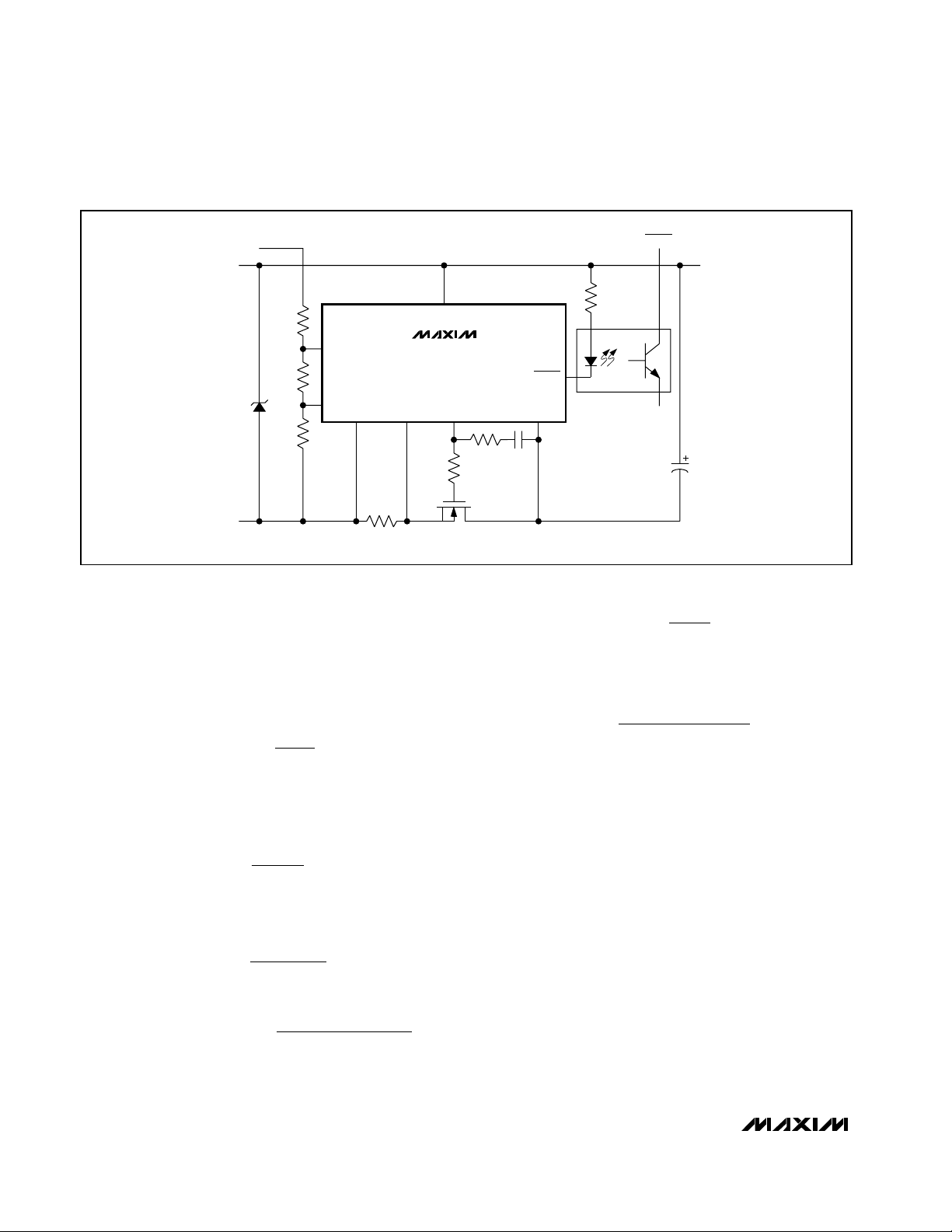
Figure 13. Using
PWRGD
to Drive an Optoisolator
-48V RTN
(SHORT PIN)
GND
R4
549kΩ
1%
UV
R5
6.49kΩ
1%
OV
V
R6
1%
EE
*DIODES INC. SMAT70A
*
10kΩ
-48V
R
SENSE
=
mV
50
I
CB
mV
Ix
INRUSH
II xI
≤−
INRUSH LOAD CB MIN
C
()
CCCx
12=+
40
08
R
245=
gd
SENSE
08..
AxC
µ
I
INRUSH
L
VV
IN MAX GS TH
() ()
V
+≤
Ior
LOAD
()
−
GS TH
()
V
DD
MAX5921A
MAX5921E
MAX5939A
MAX5939E
SENSE GATE DRAIN
Q1
IRF530
1kΩ
R3
5%
R1
0.02Ω
5%
10Ω
R2
5%
PWRGD
R7
51kΩ
5%
PWRGD
C2
15nF
100V
R
7
=
C3
100µF
100V
150
R
3
=
VV
IN NOMINAL
()
ImA
35
≤≤
LED
C
2
s
µ
2
−
Page 15
MAX5921/MAX5939
-48V Hot-Swap Controllers with External
R
SENSE
and High Gate Pulldown Current
______________________________________________________________________________________ 15
The lowest practical R
DS(ON)
, within budget constraints
and with values from 14mΩ to 540mΩ, are available at
100V breakdown.
Ensure that the temperature rise of Q1 junction is not
excessive at normal load current for the package selected. Ensure that ICBcurrent during voltage transients
does not exceed allowable transient-safe operating-area
limitations. This is determined from the SOA and transient-thermal-resistance curves in the Q1 manufacturer’s
data sheet.
Example 1:
I
LOAD
= 2.5A, efficiency = 98%, then V
DS
= 0.96V is
acceptable, or R
DS(ON)
≤ 384mΩ at operating temper-
ature is acceptable. An IRL520NS 100V NMOS with
R
DS(ON)
≤ 180mΩ and I
D(ON)
= 10A is available in
D2PAK. (A Vishay Siliconix SUD40N10-25 100V NMOS
with R
DS(ON)
≤ 25mΩ and I
D(ON)
= 40A is available in
DPAK but may be more costly because of a larger die
size).
Using the IRL520NS, VDS≤ 0.625V even at +80°C so effi-
ciency ≥ 98.6% at 80°C. PD≤ 1.56W and junction temperature rise above case temperature would be 5°C due to
the package θ
JC
= 3.1°C/W thermal resistance. Of
course, using the SUD40N10-25 will yield an efficiency
greater than 99.8% to compensate for the increased cost.
If I
CB
is set to twice I
LOAD
, or 5A, VDSmomentarily dou-
bles to ≤ 1.25V. If C
OUT
= 4000µF, transient-line input
voltage is ∆36V, the 5A charging-current pulse is:
Entering the data sheet transient-thermal-resistance
curves at 1ms provides a θ
JC
= 0.9°C/W. PD= 6.25W,
so ∆tJC= 5.6°C. Clearly, this is not a problem.
Example 2:
I
LOAD
= 10A, efficiency = 98%, allowing VDS= 0.96V
but R
DS(ON)
≤ 96mΩ. An IRF530 in a D2PAK exhibits
R
DS(ON)
≤ 90mΩ at +25°C and ≤ 135mΩ at +80°C.
Power dissipation is 9.6W at +25°C or 14.4W at +80°C.
Junction-to-case thermal resistance is 1.9W/°C, so the
junction temperature rise would be approximately 5°C
above the +25°C case temperature. For higher efficiency, consider IRL540NS with R
DS(ON)
≤ 44mΩ. This
allows η = 99%, PD≤ 4.4W, and T
JC
= +4°C
(θ
JC
= 1.1°C/W) at +25°C.
Thermal calculations for the transient condition yield
I
CB
= 20A, V
DS
= 1.8V, t = 0.5ms, transient θ
JC
=
0.12°C/W, PD= 36W and ∆t
JC
= 4.3°C.
Layout Guidelines
Good thermal contact between the MAX5921/MAX5939
and the external MOSFET is essential for the thermalshutdown feature to operate effectively. Place the
MAX5921/MAX5939 as close as possible to the drain of
the external MOSFET and use wide circuit-board traces
for good heat transfer. See Figure 15 for an example of
recommended layout for Kelvin-sensing current
through a sense resistor on a PC board.
Figure 14. MAX5921A Overcurrent Fault Example
Figure 15. Recommended Layout for Kelvin-Sensing Current
Through Sense Resistor
t1t3Ht
t2Lt
5H
4L
500µs x 128
V
OL
V
SENSE
V
GATE
Fx V
4000 1 25
t
.
µ
A
5
ms
==
1
HIGH-CURRENT PATH
SENSE RESISTOR
SENSE V
EE
MAX5921
MAX5939
Page 16

MAX5921/MAX5939
-48V Hot-Swap Controllers with External
R
SENSE
and High Gate Pulldown Current
16 ______________________________________________________________________________________
Chip Information
TRANSISTOR COUNT: 2645
PROCESS: BiCMOS
Selector Guide
Ordering Information (continued)
*Future product—contact factory for availability.
PART DCEN POLARITY FAULT MANAGEMENT
MAX5921AESA Active-Low PWRGD Autoretry 0.5 1/128
MAX5921BESA Active-High PWRGD Autoretry 0.5 1/128
MAX5921EESA Active-Low PWRGD Autoretry 2 1/128
MAX5921FESA Active-High PWRGD Autoretry 2 1/128
MAX5939AESA Active-Low PWRGD Latched 0.5 1/128
MAX5939BESA Active-High PWRGD Latched 0.5 1/128
MAX5939EESA Active-Low PWRGD Latched 2 1/128
MAX5939FESA Active-High PWRGD Latched 2 1/128
PART TEMP RANGE PIN-PACKAGE
MAX5921EESA* -40°C to +85°C 8 SO
MAX5921FESA* -40°C to +85°C 8 SO
MAX5939AESA -40°C to +85°C 8 SO
MAX5939BESA -40°C to +85°C 8 SO
MAX5939EESA* -40°C to +85°C 8 SO
MAX5939FESA* -40°C to +85°C 8 SO
MAXIMUM CURRENT-LIMIT
DURATION (ms)
MAXIMUM CURRENT-LIMIT
DUTY CYCLE
Page 17

MAX5921/MAX5939
-48V Hot-Swap Controllers with External
R
SENSE
and High Gate Pulldown Current
______________________________________________________________________________________ 17
Typical Operating Circuit
GND
-48V (INPUT1)
-48V (INPUT2)
BACKPLANE CIRCUIT CARD
GND
(SHORT PIN)
INPUT1
INPUT2
V
UV
OV
V
EE
SENSE GATE DRAIN
DD
MAX5921
MAX5939
N
PWRGD
V
+
IN
V
-
IN
LUCENT
JW050A1-E
Page 18
MAX5921/MAX5939
-48V Hot-Swap Controllers with External
R
SENSE
and High Gate Pulldown Current
Maxim cannot assume responsibility for use of any circuitry other than circuitry entirely embodied in a Maxim product. No circuit patent licenses are
implied. Maxim reserves the right to change the circuitry and specifications without notice at any time.
18 ____________________Maxim Integrated Products, 120 San Gabriel Drive, Sunnyvale, CA 94086 408-737-7600
© 2003 Maxim Integrated Products Printed USA is a registered trademark of Maxim Integrated Products.
Package Information
(The package drawing(s) in this data sheet may not reflect the most current specifications. For the latest package outline information,
go to www.maxim-ic.com/packages
.)
N
1
TOP VIEW
D
INCHES
DIM
MIN
0.053A
0.004
A1
0.014
B
0.007
C
e 0.050 BSC 1.27 BSC
0.150
HE
A
C
E
H 0.2440.228 5.80 6.20
0.016L
VARIATIONS:
INCHES
MINDIM
D
0.189 0.197 AA5.004.80 8
0.337 0.344 AB8.758.55 14
D
MAX
0.069
0.010
0.019
0.010
0.157
0.050
MAX
0.3940.386D
MILLIMETERS
MAX
MIN
1.35
1.75
0.10
0.25
0.35
0.49
0.19
0.25
3.80 4.00
0.40 1.27
MILLIMETERS
MAX
MIN
9.80 10.00
N MS012
16
AC
SOICN .EPS
e
FRONT VIEW
B
A1
L
SIDE VIEW
0-8
PROPRIETARY INFORMATION
TITLE:
PACKAGE OUTLINE, .150" SOIC
REV.DOCUMENT CONTROL NO.APPROVAL
21-0041
1
B
1
 Loading...