

Page 1
General Description
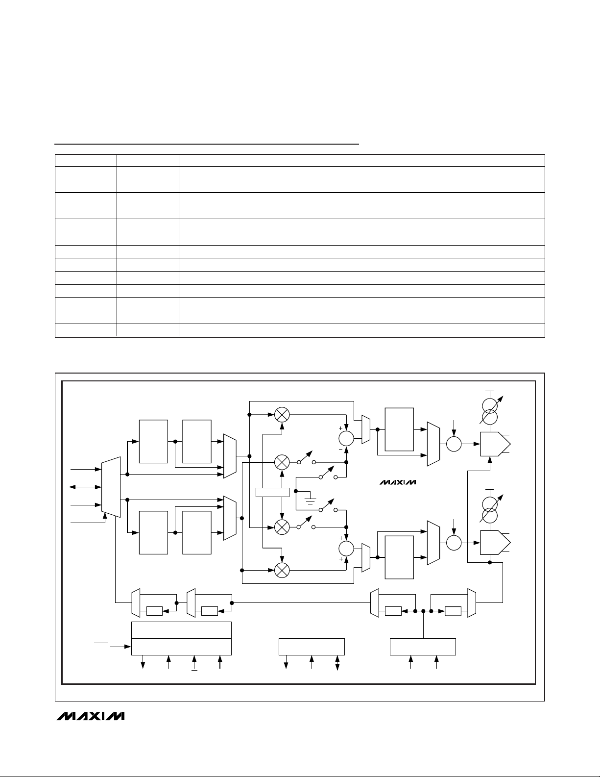
The MAX5894 programmable interpolating, modulating,
500Msps, dual digital-to-analog converter (DAC) offers
superior dynamic performance and is optimized for highperformance wideband, single-carrier transmit applications. The device integrates a selectable 2x/4x/8x
interpolating filter, a digital quadrature modulator, and
dual 14-bit, high-speed DACs on a single integrated circuit. At 30MHz output frequency and 500Msps update
rate, the in-band SFDR is 86dBc while consuming 1.1W.
The device also delivers 73dB ACLR for two-carrier
WCDMA at a 61.44MHz output frequency.
The selectable interpolating filters allow lower input data
rates while taking advantage of the high DAC update
rates. These linear-phase interpolation filters ease
reconstruction filter requirements and enhance the
passband dynamic performance. Individual offset and
gain programmability allow the user to calibrate out local
oscillator (LO) feedthrough and sideband suppression
errors generated by analog quadrature modulators.
The MAX5894 features a f
IM
/4 digital image-reject modulator. This modulator generates a quadrature-modulated IF signal that can be presented to an analog I/Q
modulator to complete the upconversion process. A
second digital modulation mode allows the signal to be
frequency-translated with image pairs at fIM/2 or fIM/4.
The MAX5894 features a standard 1.8V CMOS, 3.3V tolerant data input bus for easy interface. A 3.3V SPI™ port
is provided for mode configuration. The programmable
modes include the selection of 2x/4x/8x interpolating filters, f
IM
/2, fIM/4 or no digital quadrature modulation with
image rejection, channel gain and offset adjustment, and
offset binary or two’s complement data interface.
Pin-compatible 12- and 16-bit devices are also available.
Refer to the MAX5893 data sheet for the 12-bit version
and the MAX5895 data sheet for the 16-bit version.
Applications
Base Stations: 3G UMTS, CDMA, and GSM
Broadband Wireless Transmitters
Broadband Cable Infrastructure
Instrumentation and Automatic Test Equipment (ATE)
Analog Quadrature Modulation Architectures
Features
o 74dB ACLR at f
OUT
= 61.44MHz (Single-Carrier
WCDMA)
o Meets 3G UMTS, cdma2000
®
, GSM Spectral Masks
(f
OUT
= 122MHz)
o Noise Spectral Density = -154dBFS/Hz at
f
OUT
= 16MHz
o 91dBc SFDR at Low-IF Frequency (10MHz)
o 88dBc SFDR at High-IF Frequency (50MHz)
o Low Power: 886mW (f
CLK
= 250MHz)
o User Programmable
Selectable 2x, 4x, or 8x Interpolating Filters
< 0.01dB Passband Ripple
> 99dB Stopband Rejection
Selectable Real or Complex Modulator Operation
Selectable Modulator LO Frequency: OFF, fIM/2
or f
IM
/4
Selectable Output Filter: Lowpass or Highpass
Channel Gain and Offset Adjustment
o EV Kit Available (Order the MAX5894 EV Kit)
MAX5894
14-Bit, 500Msps, Interpolating and Modulating
Dual DAC with CMOS Inputs
________________________________________________________________
Maxim Integrated Products
1
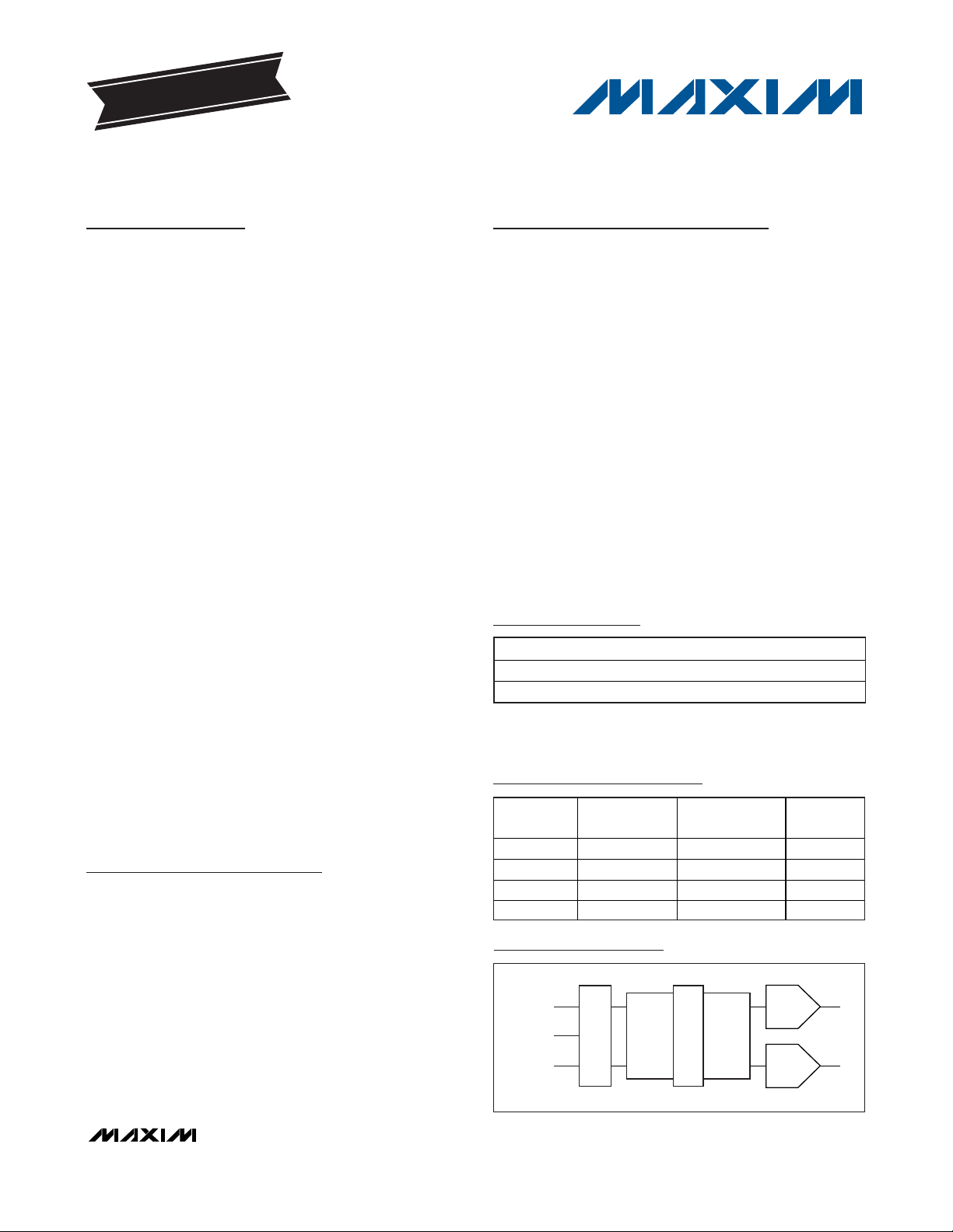
Selector Guide
Ordering Information
Simplified Diagram
19-3631; Rev 2; 10/08
For pricing, delivery, and ordering information, please contact Maxim Direct at 1-888-629-4642,
or visit Maxim’s website at www.maxim-ic.com.
Pin Configuration appears at end of data sheet.
SPI is a trademark of Motorola, Inc.
cdma2000 is a registered trademark of Telecommunications
Industry Association.
D = Dry pack.
*
EP = Exposed pad.
+
Denotes a lead-free/RoHS-compliant package.
EVALUATION KIT
AVAILABLE
PART TEMP RANGE PIN-PACKAGE
MAX5894EGK-D -40°C to +85°C 68 QFN-EP*
MAX5894EGK+D -40°C to +85°C 68 QFN-EP*
PART
MAX5893 12 500 CMOS
MAX5894 14 500 CMOS
MAX5895 16 500 CMOS
MAX5898 16 500 LVDS
RESOLUTION
(BITS)
DAC UPDATE
RATE (Msps)
DATA
PORT A
DATACLK
DATA
PORT B
DATA SYNCH
AND DEMUX
FILTERS
INTERPOLATING
1x/2x/4x
MODULATOR
FILTERS
INTERPOLATING
DAC
2x
DAC
INPUT
LOGIC
OUTI
OUTQ
Page 2
MAX5894
14-Bit, 500Msps, Interpolating and Modulating
Dual DAC with CMOS Inputs
2 _______________________________________________________________________________________
ABSOLUTE MAXIMUM RATINGS
ELECTRICAL CHARACTERISTICS
(DV
DD1.8
= AV
DD1.8
= 1.8V, AV
CLK
= AV
DD3.3
= DV
DD3.3
= 3.3V, modulator off, 2x interpolation, DATACLK output mode, dual-port
mode, 50Ω double-terminated outputs, external reference at 1.25V, T
A
= -40°C to +85°C, unless otherwise noted. Typical values are
at T
A
= +25°C, unless otherwise noted.) (Note 2)
Stresses beyond those listed under “Absolute Maximum Ratings” may cause permanent damage to the device. These are stress ratings only, and functional
operation of the device at these or any other conditions beyond those indicated in the operational sections of the specifications is not implied. Exposure to
absolute maximum rating conditions for extended periods may affect device reliability.
DV
DD1.8
, AV
DD1.8
to GND, DACREF ..................-0.3V to +2.16V
AV
DD3.3
, AV
CLK
, DV
DD3.3
to GND, DACREF........-0.3V to +3.9V
DATACLK, A0–A13, B0–B11,
SELIQ/B13, DATACLK/B12, CS, RESET, SCLK,
DIN and DOUT to GND, DACREF ...-0.3V to (DV
DD3.3
+ 0.3V)
CLKP, CLKN to GND, DACREF..............-0.3V to (AV
CLK
+ 0.3V)
REFIO, FSADJ to GND, DACREF ........-0.3V to (AV
DD3.3
+ 0.3V)
OUTIP, OUTIN, OUTQP,
OUTQN to GND, DACREF..................-1V to (AV
DD3.3
+ 0.3V)
DOUT, DATACLK, DATACLK/B12 Continuous Current........8mA
Continuous Power Dissipation (TA= +70°C)
68-Pin QFN (derate 41.7mW/°C above +70°C)
(Note 1) ...................................................................3333.3mW
Junction Temperature......................................................+150°C
Operating Temperature Range ...........................-40°C to +85°C
Storage Temperature Range .............................-65°C to +150°C
Lead Temperature (soldering, 10s) .................................+300°C
Thermal Resistance θ
JC
(Note 1)....................................0.8°C/W
Note 1: Thermal resistance based on a multilayer board with 4 x 4 via array in exposed pad area.
PARAMETER SYMBOL CONDITIONS MIN TYP MAX UNITS
STATIC PERFORMANCE
Resolution 14 Bits
Differential Nonlinearity DNL ±0.5 LSB
Integral Nonlinearity INL ±1.0 LSB
Offset Error OS -0.025 0.003 +0.025 %FS
Offset Drift ±0.03 ppm/°C
Full-Scale Gain Error GE
FS
Gain-Error Drift ±110 ppm/°C
Full-Scale Output Current I
OUTFS
Output Compliance -0.5 +1.1 V
Output Resistance R
Output Capacitance C
OUT
OUT
DYNAMIC PERFORMANCE
Maximum Clock Frequency f
Minimum Clock Frequency f
Maximum DAC Update Rate f
Minimum DAC Update Rate f
Maximum Input Data Rate f
CLK
CLK
DAC
DAC
DATA
f
= f
DAC
f
= f
DAC
f
DATACLK
f
= 16MHz, f
OUT
CLK
CLK
= 125MHz,
= 10MHz, -12dBFS
Noise Spectral Density
f
DATACLK
f
OUT
= 125MHz,
= 16MHz, f
= 10MHz, 0dBFS
-4 -0.6 +4 %FS
220mA
1MΩ
5pF
500 MHz
or f
= f
/2 500 Msps
CLK
= f
/2 1 Msps
CLK
or f
DAC
DAC
125 MWps
No interpolation -154
OFFSET
2x interpolation -154
4x interpolation -154
OFFSET
4x interpolation -151
1 MHz
dBFS/
Hz
Page 3
MAX5894
14-Bit, 500Msps, Interpolating and Modulating
Dual DAC with CMOS Inputs
_______________________________________________________________________________________ 3
ELECTRICAL CHARACTERISTICS (continued)
(DV
DD1.8
= AV
DD1.8
= 1.8V, AV
CLK
= AV
DD3.3
= DV
DD3.3
= 3.3V, modulator off, 2x interpolation, DATACLK output mode, dual-port
mode, 50Ω double-terminated outputs, external reference at 1.25V, T
A
= -40°C to +85°C, unless otherwise noted. Typical values are
at T
A
= +25°C, unless otherwise noted.) (Note 2)
PARAMETER SYMBOL CONDITIONS MIN TYP MAX UNITS
In-Band SFDR
(DC to f
DATA
/2)
SFDR
Two-Tone IMD TTIMD
f
DATACLK
= 125MHz,
interpolation off, 0dBFS
f
DATACLK
= 125MHz,
2x interpolation, 0dBFS
f
DATACLK
= 125MHz,
4x interpolation, 0dBFS
f
DATACLK
f
OUT1
= 125MHz,
= 9MHz, f
10MHz, -6.1dBFS
f
= 125MHz, f
DATA
= 79MHz, f
OUT2
80MHz, -6.1dBFS
f
DATACLK
f
OUT1
= 62.5MHz,
= 9MHz, f
10MHz, -6.1dBFS
OUT2
=
OUT2
f
= 10MHz 91
OUT
f
= 30MHz 85
OUT
= 50MHz 73
f
OUT
f
= 10MHz 77 89
OUT
f
= 30MHz 86
OUT
f
= 50MHz 85
OUT
f
= 10MHz 91
OUT
f
= 30MHz 86
OUT
f
= 50MHz 88
OUT
No interpolation -102
2x interpolation -102
=
4x interpolation -102
2x interpolation,
f
OUT1
/4 complex
IM
modulation
-73
4x interpolation,
/4 complex
f
IM
-75
modulation
=
8x interpolation -99
dBc
dBc
Four-Tone IMD FTIMD
ACLR for WCDMA
(Note 3)
ACLR
f
DATACLK
f
OUT1
= 70MHz, -6.1dBFS
f
DATACLK
f
OUT1
= 180MHz, -6.1dBFS
f
DATACLK
= 62.5MHz,
= 69MHz, f
= 62.5MHz,
= 179MHz, f
= 125MHz, f
OUT2
OUT2
8x interpolation,
/4 complex
f
IM
modulation
8x, highpass
interpolation,
f
/4 complex
IM
modulation
spaced 1MHz
OUT
apart from 32MHz, -12dBFS, 2x
interpolation
f
DATACLK
f
OUT
f
DATACLK
= 61.44MHz,
= baseband
=
122.88MHz, f
61.44MHz
f
DATACLK
=
122.88MHz, f
122.88MHz
OUT
OUT
=
=
4x interpolation 78
8x interpolation 78
2x interpolation,
fIM/4 complex
modulation
4x interpolation,
fIM/4 complex
modulation
-70
-63
-95 dBc
74
dB
69
Page 4
MAX5894
14-Bit, 500Msps, Interpolating and Modulating
Dual DAC with CMOS Inputs
4 _______________________________________________________________________________________
ELECTRICAL CHARACTERISTICS (continued)
(DV
DD1.8
= AV
DD1.8
= 1.8V, AV
CLK
= AV
DD3.3
= DV
DD3.3
= 3.3V, modulator off, 2x interpolation, DATACLK output mode, dual-port
mode, 50Ω double-terminated outputs, external reference at 1.25V, T
A
= -40°C to +85°C, unless otherwise noted. Typical values are
at T
A
= +25°C, unless otherwise noted.) (Note 2)
Output Propagation Delay t
Output Rise Time t
Output Fall Time t
Output Settling Time To 0.5% (Note 5) 11 ns
Output Bandwidth -1dB bandwidth (Note 6) 240 MHz
Passband Width Ripple < -0.01dB
Stopband Rejection
Data Latency
DAC INTERCHANNEL MATCHING
Gain Match ∆Gain f
Gain-Match Tempco ∆Gain/°C I
Phase Match ∆Phase f
Phase-Match Tempco ∆Phase/°C f
DC Gain Match I
Channel-to-Channel Crosstalk f
REFERENCE
Reference Input Range 0.125 1.250 V
Reference Output Voltage V
Reference Input Resistance R
Reference Voltage Drift ±50 ppm/°C
CMOS LOGIC INPUT/OUTPUT (A13–A0, SELIQ/B13, DATACLK/B12, B11–B0, DATACLK)
Input High Voltage V
Input Low Voltage V
Input Current I
Input Capacitance C
PARAMETER SYMBOL CONDITIONS MIN TYP MAX UNITS
PD
RISE
FALL
REFIO
REFIO
IH
IL
IN
IN
1x interpolation (Note 4) 2.9 ns
10% to 90% (Note 5) 0.75 ns
10% to 90% (Note 5) 1 ns
0.604 x f
0.604 x f
0.604 x f
1x interpolation 22
2x interpolation 70
4x interpolation 146
8x interpolation 311
Internal reference 1.14 1.20 1.27 V
DATA
DATA
DATA
= DC - 80MHz, I
OUT
= 20mA ±0.02 ppm/°C
OUTFS
= 60MHz, I
OUT
= 60MHz, I
OUT
= 20mA -0.25 0.04 +0.25 dB
OUTFS
= 50MHz, f
OUT
0.4 x
f
DATA
, 2x interpolation 100
, 4x interpolation 100
, 8x interpolation 100
= 20mA ±0.1 dB
OUTFS
= 20mA ±0.13 Deg
OUTFS
= 20mA ±0.006 Deg/°C
OUTFS
= 250MHz, 0dBFS -90 dB
DAC
10 kΩ
0.7 x
DV
DD1.8
0.3 x
DV
-20 ±1 +20 µA
3pF
DD1.8
dB
Clock
Cycles
V
V
Page 5
MAX5894
14-Bit, 500Msps, Interpolating and Modulating
Dual DAC with CMOS Inputs
_______________________________________________________________________________________ 5
ELECTRICAL CHARACTERISTICS (continued)
(DV
DD1.8
= AV
DD1.8
= 1.8V, AV
CLK
= AV
DD3.3
= DV
DD3.3
= 3.3V, modulator off, 2x interpolation, DATACLK output mode, dual-port
mode, 50Ω double-terminated outputs, external reference at 1.25V, T
A
= -40°C to +85°C, unless otherwise noted. Typical values are
at T
A
= +25°C, unless otherwise noted.) (Note 2)
Output High Voltage V
Output Low Voltage V
Output Leakage Current Three-state 1 µA
Rise/Fall Time C
CLOCK INPUT (CLKP, CLKN)
Differential Input Voltage Swing V
Differential Input Slew Rate > 100 V/µs
Common-Mode Voltage V
Input Resistance R
Input Capacitance C
Minimum Clock Duty Cycle 45 %
Maximum Clock Duty Cycle 55 %
CLKP/CLKN, DATACLK TIMING (Figure 4) (Notes 7, 8)
CLK to DATACLK Delay t
Data Hold Time, DATACLK
Input/Output (Pin 14)
Data Setup Time, DATACLK
Input/Output (Pin 14)
Data Hold Time, DATACLK/B10
Input/Output (Pin 27)
Data Setup Time, DATACLK/B10
Input/Output (Pin 27)
SERIAL-PORT INTERFACE TIMING (Figure 3) (Note 7)
SCLK Frequency f
CS Setup Time t
Input Hold Time t
Input Setup Time t
Data Valid Duration t
PARAMETER SYMBOL CONDITIONS MIN TYP MAX UNITS
OH
OL
DIFF
COM
CLK
CLK
D
t
DH
t
DS
t
DH
t
DS
SCLK
SS
SDH
SDS
SDV
200µA load
200µA load
Sine-wave input > 1.5
Square-wave input > 0.5
AC-coupled AV
DATACLK output mode, C
Capturing rising edge 1.0
Capturing falling edge 2.1
Capturing rising edge 0.4
Capturing falling edge -0.7
Capturing rising edge 1.0
Capturing falling edge 2.3
Capturing rising edge 0.2
Capturing falling edge -0.4
= 10pF, 20% to 80% 1.6 ns
LOAD
0.8 x
DV
DD3.3
= 10pF 6.2 ns
LOAD
2.5 ns
0ns
4.5 ns
6.5 16.5 ns
0.2 x
DV
DD3.3
/2 V
CLK
5kΩ
3pF
10 MHz
V
V
V
P-P
ns
ns
ns
ns
Page 6
MAX5894
14-Bit, 500Msps, Interpolating and Modulating
Dual DAC with CMOS Inputs
6 _______________________________________________________________________________________
ELECTRICAL CHARACTERISTICS (continued)
(DV
DD1.8
= AV
DD1.8
= 1.8V, AV
CLK
= AV
DD3.3
= DV
DD3.3
= 3.3V, modulator off, 2x interpolation, DATACLK output mode, dual-port
mode, 50Ω double-terminated outputs, external reference at 1.25V, T
A
= -40°C to +85°C, unless otherwise noted. Typical values are
at T
A
= +25°C, unless otherwise noted.) (Note 2)
Note 2: All limit specifications are 100% tested at T
A
≥ +25°C. Specifications at TA< +25°C are guaranteed by design and characterization.
Note 3: 3.84MHz bandwidth, single carrier.
Note 4: Excludes data latency.
Note 5: Measured single-ended into a 50Ω load.
Note 6: Excludes sin(x)/x rolloff.
Note 7: Guaranteed by design and characterization.
Note 8: Setup and hold time specifications characterized with 3.3V CMOS logic levels.
Note 9: Parameter defined as the change in midscale output caused by a ±5% variation in the nominal supply voltage.
PARAMETER SYMBOL CONDITIONS MIN TYP MAX UNITS
POWER SUPPLIES
Digital Supply Voltage DV
Digital I/O Supply Voltage DV
Clock Supply Voltage AV
Analog Supply Voltage
AV
AV
I
AVDD3.3
Analog Supply Current
I
AVDD1.8
Digital Supply Current I
Digital I/O Supply Current I
Clock Supply Current I
DVDD1.8
DVDD3.3
AVCLK
Total Power Dissipation P
Power-Down Current
AV
Ratio
Power-Supply Rejection
DD3.3
PSRR
DD1.8
DD3.3
CLK
DD3.3
DD1.8
TOTAL
1.71 1.8 1.89 V
3.0 3.3 3.6 V
3.135 3.3 3.465 V
3.135 3.3 3.465
1.71 1.8 1.89
f
= 250MHz, 2x interpolation, 0dBFS,
CLK
f
= 10MHz
OUT
f
= 250MHz, 2x interpolation, 0dBFS,
CLK
f
= 10MHz
OUT
f
= 250MHz, 2x interpolation, 0dBFS,
CLK
= 10MHz
f
OUT
f
= 250MHz, 2x interpolation, 0dBFS,
CLK
= 10MHz
f
OUT
f
= 250MHz, 2x interpolation, 0dBFS,
CLK
= 10MHz
f
OUT
f
= 250MHz, 2x interpolation, 0dBFS,
CLK
= 10MHz
f
OUT
AV
DD3.3
AV
DV
DV
AV
DD1.8
DD1.8
DD3.3
CLK
All I/O are static high or
low, bit 2 to bit 4 of
address 00h are set high
(Note 9) 0.05 %FS/V
A
110 130
27 32
225 250 mA
21 32 mA
35mA
886 mW
450
1
10
100
1
V
mA
µA
Page 7
MAX5894
14-Bit, 500Msps, Interpolating and Modulating
Dual DAC with CMOS Inputs
_______________________________________________________________________________________
7
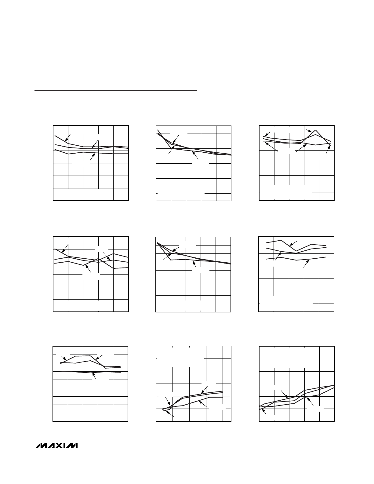
Typical Operating Characteristics
(DV
DD1.8
= AV
DD1.8
= 1.8V, AV
CLK
= AV
DD3.3
= DV
DD3.3
= 3.3V, modulator off, 2x interpolation, output is transformer-coupled to
50Ω load, T
A
= +25°C, unless otherwise noted.)
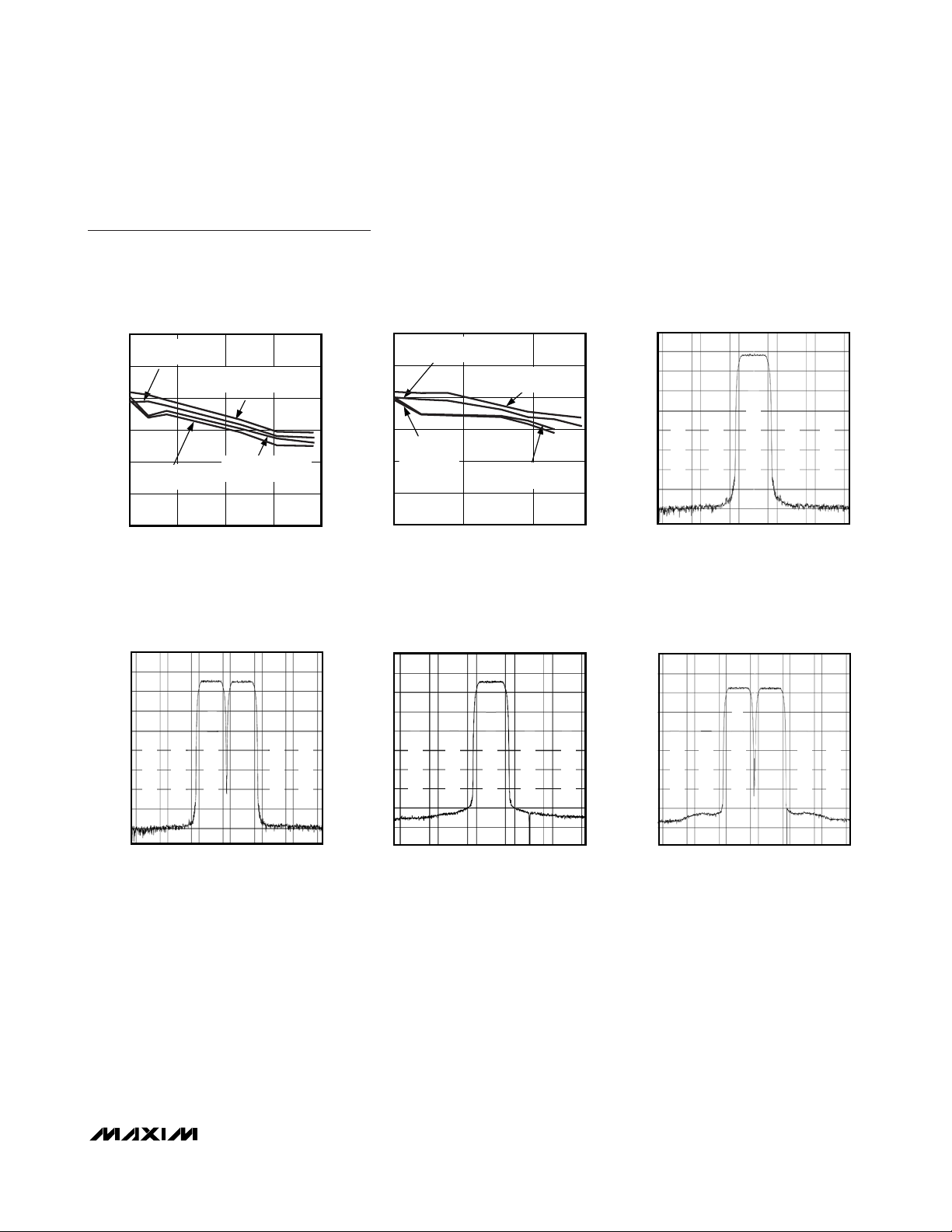
IN-BAND SFDR vs. OUTPUT FREQUENCY
f
120
100
80
60
SFDR (dBc)
40
20
0
050
IN-BAND SFDR vs. OUTPUT FREQUENCY
f
120
100
80
60
SFDR (dBc)
40
20
0
050
DATA
SPURS MEASURED BETWEEN
0MHz AND 62.5MHz
DATA
-0.1dBFS
SPURS MEASURED BETWEEN
0MHz AND 62.5MHz
= 125Mwps, 2x INTERPOLATION
-0.1dBFS
-6dBFS
-12dBFS
40302010
OUTPUT FREQUENCY (MHz)
= 125Mwps, 4x INTERPOLATION
-6dBFS
-12dBFS
40302010
OUTPUT FREQUENCY (MHz)
MAX5894 toc01
MAX5894 toc04
100
SFDR (dBc)
SFDR (dBc)
0UT-OF-BAND SFDR vs. OUTPUT FREQUENCY
= 125Mwps, 2x INTERPOLATION
f
DATA
90
80
70
60
50
40
30
20
10
0
-0.1dBFS
MAX5894 toc02
-6dBFS
SPURS MEASURED BETWEEN
62.5MHz AND 125MHz
050
OUTPUT FREQUENCY (MHz)
-12dBFS
40302010
OUT-OF-BAND SFDR vs. OUTPUT FREQUENCY
= 125Mwps, 4x INTERPOLATION
f
DATA
90
80
70
60
-6dBFS
50
40
30
20
SPURS MEASURED BETWEEN
10
62.5MHz AND 250MHz
0
050
-0.1dBFS
MAX5894 toc05
-12dBFS
40302010
OUTPUT FREQUENCY (MHz)
IN-BAND SFDR vs. OUTPUT FREQUENCY
f
DATA
90
-6dBFS
80
70
60
50
40
SFDR (dBc)
30
20
UPPER SIDEBAND MODULATION
SPURS MEASURED BETWEEN
10
62.5MHz AND 125MHz
0
62.5 112.5
IN-BAND SFDR vs. OUTPUT FREQUENCY
f
DATA
90
80
70
60
-6dBFS
50
40
SFDR (dBc)
30
20
LOWER SIDEBAND MODULATION
10
SPURS MEASURED BETWEEN
62.5MHz AND 125MHz
0
75 125
= 125Mwps, 2x INTERPOLATION
-0.1dBFS
MAX5894 toc03
-12dBFS
-0.1dBFS
102.592.582.572.5
OUTPUT FREQUENCY (MHz)
= 125Mwps, 4x INTERPOLATION
-0.1dBFS
MAX5894 toc06
-12dBFS
1151059585
OUTPUT FREQUENCY (MHz)
IN-BAND SFDR vs. OUTPUT FREQUENCY
90
-0.1dBFS
80
70
60
50
40
SFDR (dBc)
30
20
UPPER SIDEBAND MODULATION
SPURS MEASURED BETWEEN
10
125MHz AND 187.5MHz
0
125 175
OUTPUT FREQUENCY (MHz)
-6dBFS
-12dBFS
= 125Mwps, 4x INTERPOLATION
f
DATA
TWO-TONE IMD vs. OUTPUT FREQUENCY
= 125Mwps, 2x INTERPOLATION
f
DATA
0
1MHz CARRIER SPACING
COMPLEX MODULATION FOR
-20
MAX5894 toc07
165155145135
OUTPUT FREQUENCIES
GREATER THAN 50MHz
-40
-60
-9dBFS
-80
TWO-TONE IMD (dBc)
-100
-120
0
-6dBFS
-12dBFS
-6dBFS
CENTER FREQUENCY (MHz)
MAX5894 toc08
100755025
TWO-TONE IMD vs. OUTPUT FREQUENCY
= 125Mwps, 4x INTERPOLATION
f
DATA
0
1MHz CARRIER SPACING
COMPLEX MODULATION FOR
-20
OUTPUT FREQUENCIES
GREATER THAN 50MHz
-40
-60
-80
TWO-TONE IMD (dBc)
-100
-120
-9dBFS
-12dBFS
-6dBFS
10
CENTER FREQUENCY (MHz)
MAX5894 toc09
1601301007040
Page 8
MAX5894
14-Bit, 500Msps, Interpolating and Modulating
Dual DAC with CMOS Inputs
8 _______________________________________________________________________________________
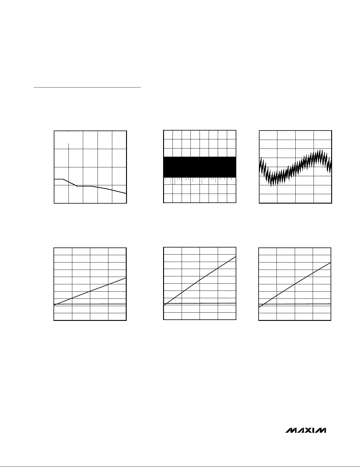
4
Typical Operating Characteristics (continued)
(DV
DD1.8
= AV
DD1.8
= 1.8V, AV
CLK
= AV
DD3.3
= DV
DD3.3
= 3.3V, modulator off, 2x interpolation, output is transformer-coupled to
50Ω load, T
A
= +25°C, unless otherwise noted.)
GAIN MISMATCH vs. TEMPERATURE
= 125Mwps, 2x INTERPOLATION
f
DATA
0.100
f
= 22.7MHz
OUT
= -6dBFS
A
GAIN MISMATCH (dB)
OUT
0.075
0.050
0.025
0
-40 85
TEMPERATURE (°C)
SUPPLY CURRENT vs. DAC UPDATE RATE
2x INTERPOLATION, f
500
450
400
350
300
250
200
150
SUPPLY CURRENT (mA)
100
50
0
100 300
1.8V TOTAL
f
DAC
3.3V TOTAL
(MHz)
OUT
603510-15
= 5MHz
250200150
MAX5894 toc10
MAX5894 toc13
DIFFERENTIAL NONLINEARITY
vs. DIGITAL INPUT CODE
1.00
0.75
0.50
0.25
0
DNL (LSB)
-0.25
-0.50
-0.75
-1.00
0 16,38
DIGITAL INPUT CODE
12,28881924096
SUPPLY CURRENT vs. DAC UPDATE RATE
4x INTERPOLATION, f
500
450
400
350
300
250
200
150
SUPPLY CURRENT (mA)
100
50
0
100 500
f
DAC
OUT
1.8V TOTAL
3.3V TOTAL
(MHz)
= 5MHz
400300200
INTEGRAL NONLINEARITY
vs. DIGITAL INPUT CODE
2.0
1.5
MAX5894 toc11
1.0
0.5
0
INL (LSB)
-0.5
-1.0
-1.5
-2.0
0 16,384
DIGITAL INPUT CODE
SUPPLY CURRENT vs. DAC UPDATE RATE
8x INTERPOLATION, f
500
450
MAX5894 toc14
400
350
300
250
200
150
SUPPLY CURRENT (mA)
100
50
0
100 500
f
(MHz)
DAC
OUT
1.8V TOTAL
3.3V TOTAL
MAX5894 toc12
12,28881924096
= 5MHz
MAX5894 toc15
400300200
Page 9
MAX5894
14-Bit, 500Msps, Interpolating and Modulating
Dual DAC with CMOS Inputs
_______________________________________________________________________________________
9
Typical Operating Characteristics (continued)
(DV
DD1.8
= AV
DD1.8
= 1.8V, AV
CLK
= AV
DD3.3
= DV
DD3.3
= 3.3V, modulator off, 2x interpolation, output is transformer-coupled to
50Ω load, T
A
= +25°C, unless otherwise noted.)
WCDMA ACLR vs. OUTPUT FREQUENCY
f
DATA
= 122.88Mwps, 4x INTERPOLATION
MAX5894 toc16
f
CENTER
(MHz)
ACLR (dB)
1208040
50
60
70
80
90
100
40
0 160
TWO-CARRIER
ADJACENT CHANNEL
ONE-CARRIER
ADJACENT CHANNEL
TWO-CARRIER
ALTERNATE CHANNEL
ONE-CARRIER
ALTERNATE CHANNEL
WCDMA ACLR vs. OUTPUT FREQUENCY
f
DATA
= 76.8Mwps, 4x INTERPOLATION
MAX5894 toc17
f
CENTER
(MHz)
ACLR (dB)
8040
50
60
70
80
90
100
40
0
ONE-CARRIER
ALTERNATE CHANNEL
ONE-CARRIER
ADJACENT CHANNEL
TWO-CARRIER
ALTERNATE CHANNEL
TWO-CARRIER
ADJACENT
CHANNEL
MAX5894 toc18
WCDMA ACLR SPECTRAL PLOT
f
DATA
= 61.44Mwps, 8x INTERPOLATION
f
CENTER
= 61.44MHz
SPAN = 25.5MHz
ACLR2 = 78dB
OUTPUT POWER (dBm)
ACLR1 = 76dB
ACLR1 = 75dB
ACLR2 = 77dB
CARRIER = -11dBm
-110
-100
-90
-80
-70
-60
-50
-40
-30
-20
TWO-CARRIER WCDMA ACLR SPECTRAL PLOT
= 61.44Mwps, 8x INTERPOLATION
f
DATA
-20
-30
-40
-50
-60
-70
-80
-90
OUTPUT POWER (dBm)
-100
-110
ACLR1 = 74dB
ACLR2 = 75dB
CARRIER = -14dBm
ACLR1 = 73dB
MAX5894 toc19
ACLR2 = 74dB
-20
-30
-40
-50
-60
-70
-80
-90
OUTPUT POWER (dBm)
-100
-110
WCDMA ACLR SPECTRAL PLOT
= 122.88Mwps, 4x INTERPOLATION
f
DATA
ACLR1 = 67dB
ACLR2 = 70dB
CARRIER = -14dBm
ACLR2 = 69dB
ACLR1 = 67dB
MAX5894 toc20
TWO-CARRIER WCDMA ACLR SPECTRAL PLOT
= 122.88Mwps, 4x INTERPOLATION
f
DATA
-20
-30
-40
-50
-60
-70
-80
-90
OUTPUT POWER (dBm)
-100
-110
ACLR1 = 65dB
ACLR2 = 68dB
CARRIER = -17dBm
ACLR1 = 65dB
MAX5894 toc21
ACLR2 = 67dB
f
= 61.44MHz
CENTER
SPAN = 30.5MHz
f
= 122.88MHz
CENTER
SPAN = 25.5MHz
f
= 122.88MHz
CENTER
SPAN = 30.5MHz
Page 10
MAX5894
14-Bit, 500Msps, Interpolating and Modulating
Dual DAC with CMOS Inputs
10 ______________________________________________________________________________________
Pin Description
PIN NAME FUNCTION
1 CLKP Noninverting Differential Clock Input. Internally biased to AV
2 CLKN Inverting Differential Clock Input. Internally biased to AV
3, 4, 5, 24, 25,
42, 43
6, 21, 30, 37 DV
7–12, 15–20,
22, 23
13, 44 DV
14 DATACLK Programmable Data Clock Input/Output. See the DATACLK Modes section for details.
26 SELIQ/B13
27 DATACLK/B12
28, 29, 31–36,
38–41
45 DOUT Serial-Port Data Output
46 DIN Serial-Port Data Input
47 SCLK Serial-Port Clock Input. Data on DIN is latched on the rising edge of SCLK.
48 CS Serial-Port Interface Select. Drive CS low to enable serial-port interface.
49 RESET Reset Input. Set RESET low during power-up.
50 REFIO Reference Input/Output. Bypass to ground with a 1µF capacitor as close to the pin as possible.
51 DACREF
52 FSADJ
N.C. Internally Connected. Do not connect.
DD1.8
A13–A0
DD3.3
B11–B0
Digital Power Supply. Accepts a 1.71V to 1.89V supply range. Bypass each pin to ground with a
0.1µF capacitor as close to the pin as possible.
A-Port Data Inputs.
Dual-port mode:
I-channel data input. Data is latched on the rising/falling edge (programmable) of the DATACLK.
Single-port mode:
I-channel and Q-channel data input, with SELIQ.
CMOS I/O Power Supply. Accepts a 3.0V to 3.6V supply range. Bypass each pin to ground with a
0.1µF capacitor as close to the pin as possible.
Select I-/Q-Channel Input or B-Port MSB Input.
Single-port mode:
If SELIQ = LOW, data is latched into Q-channel on the rising/falling edge (programmable) of
the DATACLK.
If SELIQ = HIGH, data is latched into I-channel on the rising/falling edge (programmable) of the
DATACLK.
Dual-port mode:
Q-channel MSB input.
Alternate DATACLK Input/Output or B-Port Bit 12 Input.
Single-port mode:
See the DATACLK Modes section for details.
Dual-port mode:
Q-channel bit 12 input.
If unused connect to GND.
B-Port Data Bits 11–0.
Dual-port mode:
Q-channel inputs. Data is latched on the rising/falling (programmable) edge of the DATACLK.
Single-port mode:
Connect to GND.
C ur r ent- S et Resi stor Retur n P ath. For a 20m A ful l - scal e outp ut cur r ent, connect a 2kΩ r esi stor b etw een
FS AD J and D AC RE F. Inter nal l y connected to GN D . D O NO T U SE A S A N EXT ER N A L G R O U N D
C O N N EC T IO N .
Full-Scale Adjust Input. This input sets the full-scale output current of the DAC. For a 20mA fullscale output current, connect a 2kΩ resistor between FSADJ and DACREF.
CLK
CLK
/2.
/2.
Page 11
MAX5894
14-Bit, 500Msps, Interpolating and Modulating
Dual DAC with CMOS Inputs
______________________________________________________________________________________ 11
Pin Description (continued)
Functional Diagram
PIN NAME FUNCTION
53, 67 AV
54, 56, 59, 61,
64, 66
55, 60, 65 AV
DD1.8
GND Ground
DD3.3
57 OUTQN Inverting Differential DAC Current Output for Q-Channel
58 OUTQP Noninverting Differential DAC Current Output for Q-Channel
62 OUTIN Inverting Differential DAC Current Output for I-Channel
63 OUTIP Noninverting Differential DAC Current Output for I-Channel
68 AV
CLK
— EP Exposed Pad. Must be connected to GND through a low-impedance path.
INTERPOLATING
FILTER
A0–A13
DATACLK
B0–B13
SELIQ
DATA SYNCH
AND DEMUX
INTERPOLATING
FILTER
Low Analog Power Supply. Accepts a 1.71V to 1.89V supply range. Bypass each pin to GND with
a 0.1µF capacitor as close to the pin as possible.
Analog Power Supply. Accepts a 3.135V to 3.465V supply range. Bypass each pin to GND with a
0.1µF capacitor as close to the pin as possible.
Clock Power Supply. Accepts a 3.135V to 3.465V supply range. Bypass to ground with a 0.1µF
capacitor as close to the pin as possible.
MODULATOR
INTERPOLATING
INTERPOLATING
FILTER
2x
2x
FILTER
INTERPOLATING
2x
MUX
I
Q
fIM/2, fIM/4
I
MUX
2x
Q
∑
∑
FILTER
MAX5894
INTERPOLATING
FILTER
DIGITAL
OFFSET
MUX
MUX
ADJUST
∑
DIGITAL
OFFSET
ADJUST
2x
∑
2x
IDAC
QDAC
f
DAC
DIGITAL
GAIN
ADJUST
OUTIP
OUTIN
DIGITAL
GAIN
ADJUST
OUTQP
OUTQN
RESET
f
DAC
/2/2
CONTROL REGISTERS
SERIAL INTERFACE
DOUT DIN CS SCLK DACREF FSADJ REFIO
REFERENCE
CLOCK BUFFERS
AND DIVIDERS
/2/2
f
CLK
CLKPCLKN
Page 12
MAX5894
14-Bit, 500Msps, Interpolating and Modulating
Dual DAC with CMOS Inputs
12 ______________________________________________________________________________________
Detailed Description
The MAX5894 dual, 500Msps, high-speed, 14-bit, current-output DAC provides superior performance in
communication systems requiring low-distortion analog-signal reconstruction. The MAX5894 combines two
DAC cores with 8x/4x/2x/1x programmable digital interpolation filters, a digital quadrature modulator, an SPIcompatible serial interface for programming the device,
and an on-chip 1.20V reference. The full-scale output
current range is programmable from 2mA to 20mA to
optimize power dissipation and gain control.
Each channel contains three selectable interpolating filters making the MAX5894 capable of 1x, 2x, 4x, or 8x
interpolation, which allows for low input data rates and
high DAC update rates. When operating in 8x interpolation mode, the interpolator increases the DAC conversion rate by a factor of eight, providing an eight-fold
increase in separation between the reconstructed
waveform spectrum and its first image. The MAX5894
accepts either two’s complement or offset binary input
data format and can operate from either a single- or
dual-port input bus.
The MAX5894 includes modulation modes at f
IM
/2 and
fIM/4, where fIMis the data rate at the input of the modulator. If 2x interpolation is used, this data rate is 2x the
input data rate. If 4x or 8x interpolation is used, this data
rate is 4x the input data rate. Table 1 summarizes the
modulator operating data rates for dual-port mode.
The power-down modes can be used to turn off each
DAC’s output current or the entire digital section.
Programming both DACs into power-down simultaneously automatically powers down the digital interpolator
filters. Note the SPI section is always active.
The analog and digital sections of the MAX5894 have
separate power-supply inputs (AV
DD3.3
, AV
DD1.8
,
AV
CLK
, DV
DD3.3
, and DV
DD1.8
), which minimize noise
coupling from one supply to the other. AV
DD1.8
and
DV
DD1.8
operate from a typical 1.8V supply, and all
other supply inputs operate from a typical 3.3V supply.
Serial Interface
The SPI-compatible serial interface programs the
MAX5894 registers. The serial interface consists of the
CS, DIN, SCLK, and DOUT. Data is shifted into DIN on
the rising edge of the SCLK when CS is low. When CS
is high, data presented at DIN is ignored and DOUT is
in high-impedance mode. Note: CS must transition
high after each read/write operation. DOUT is the
serial data output for reading registers to facilitate easy
debugging during development. DIN and DOUT can
be connected together to form a 3-wire serial interface
bus or remain separate and form a 4-wire SPI bus.
The serial interface supports two-byte transfer in a
communication cycle. The first byte is a control byte
written to the MAX5894 only. The second byte is a data
byte and can be written to or read from the MAX5894.
Table 1. Quadrature Modulator Operating Data Rates (fIMis the Data Rate at the Input of
the Modulator) for Dual-Port Mode
INTERPOLATION RATE MODULATION MODE (fLO)
1x
2x
4x
8x
fIM/2 f
f
/4 f
IM
fIM/2 f
f
/4 f
IM
fIM/2 f
/4 f
f
IM
fIM/2 f
/4 f
f
IM
MODULATION FREQUENCY
RELATIVE TO f
DAC
DAC
DAC
DAC
DAC
DAC
DAC
DAC
DAC
/2 f
/4 f
/2 f
/4 f
/2 2 x f
/4 f
/4 2 x f
/8 f
MODULATION FREQUENCY
RELATIVE TO f
DATA
DATA
DATA
DATA
/2
/4
DATA
/2
DATA
DATA
DATA
DATA
Page 13
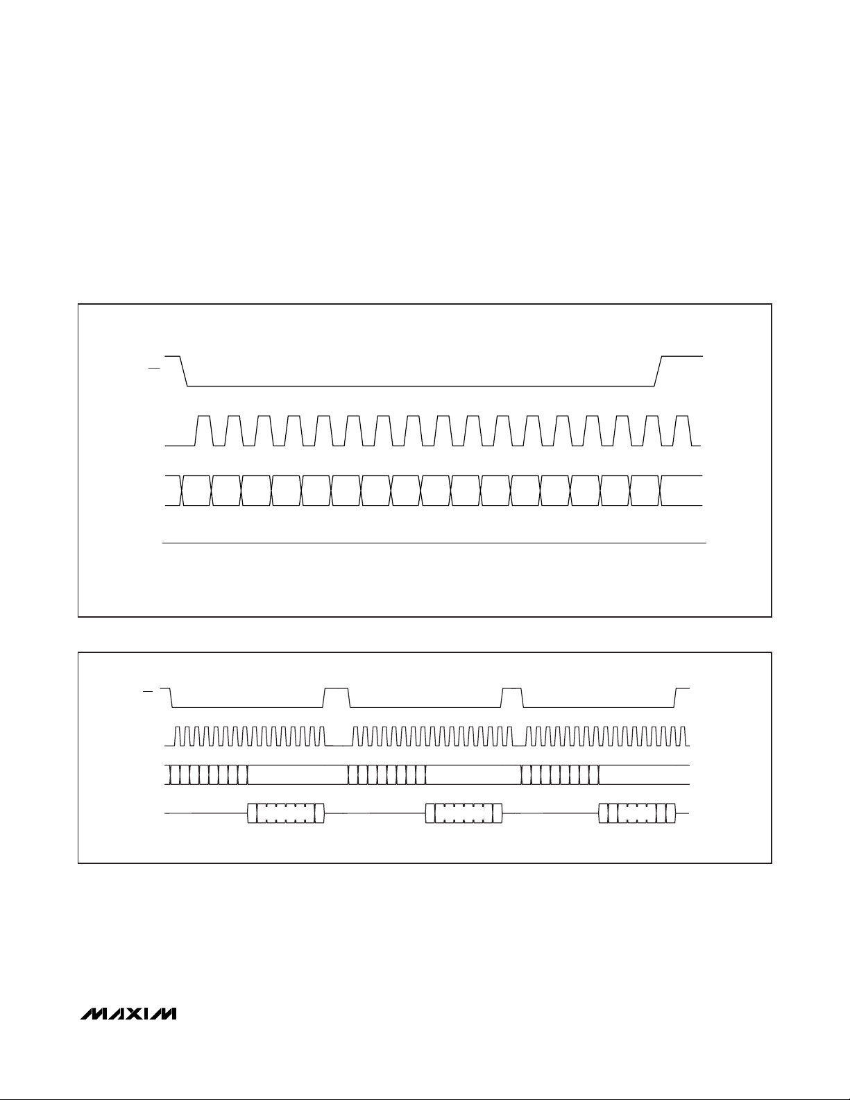
When writing to the MAX5894, data is shifted into DIN;
data is shifted out of DOUT in a read operation. Bits 0 to
3 of the control byte are the address bits. These bits set
the address of the register to be written to or read from.
Bits 4 to 6 of the control byte must always be set to 0.
Bit 7 is a read/write bit: 0 for write operation and 1 for
read operation. The most significant bit (MSB) is shifted
in first in default mode. If the serial port is set to LSB-first
mode, both the control byte and data byte are shifted LSB
in first. Figures 1 and 2 show the SPI serial-interface operation in the default write and read mode, respectively.
Figure 3 is a timing diagram for the SPI serial interface.
MAX5894
14-Bit, 500Msps, Interpolating and Modulating
Dual DAC with CMOS Inputs
______________________________________________________________________________________ 13
Figure 1. SPI Serial-Interface Write Cycle, MSB-First Mode
Figure 2. SPI Serial-Interface Read Cycle, MSB-First Mode
CS
SCLK
DIN
DOUT
0 0 0 0 A3 A2 A1 A0 D7 D6 D5 D4 D3 D2 D1 D0
HIGH IMPEDANCE
CS
SCLK
DIN
DOUT
READ CYCLE N - 1
ADDRESS DATA
10003210
HIGH
IMPEDANCE
IGNORED
DATA N - 2
ADDRESS DATA
10003210
HIGH
IMPEDANCE
READ CYCLE N
IGNORED
DATA N - 1
READ CYCLE N + 1
ADDRESS DATA
10003210
HIGH
IMPEDANCE
IGNORED
DATA N
Page 14

MAX5894
14-Bit, 500Msps, Interpolating and Modulating
Dual DAC with CMOS Inputs
14 ______________________________________________________________________________________
Figure 3. SPI Serial-Interface Timing Diagram
t
SS
CS
SCLK
DIN
DOUT
t
SDS
t
SDH
t
SDV
Page 15
MAX5894
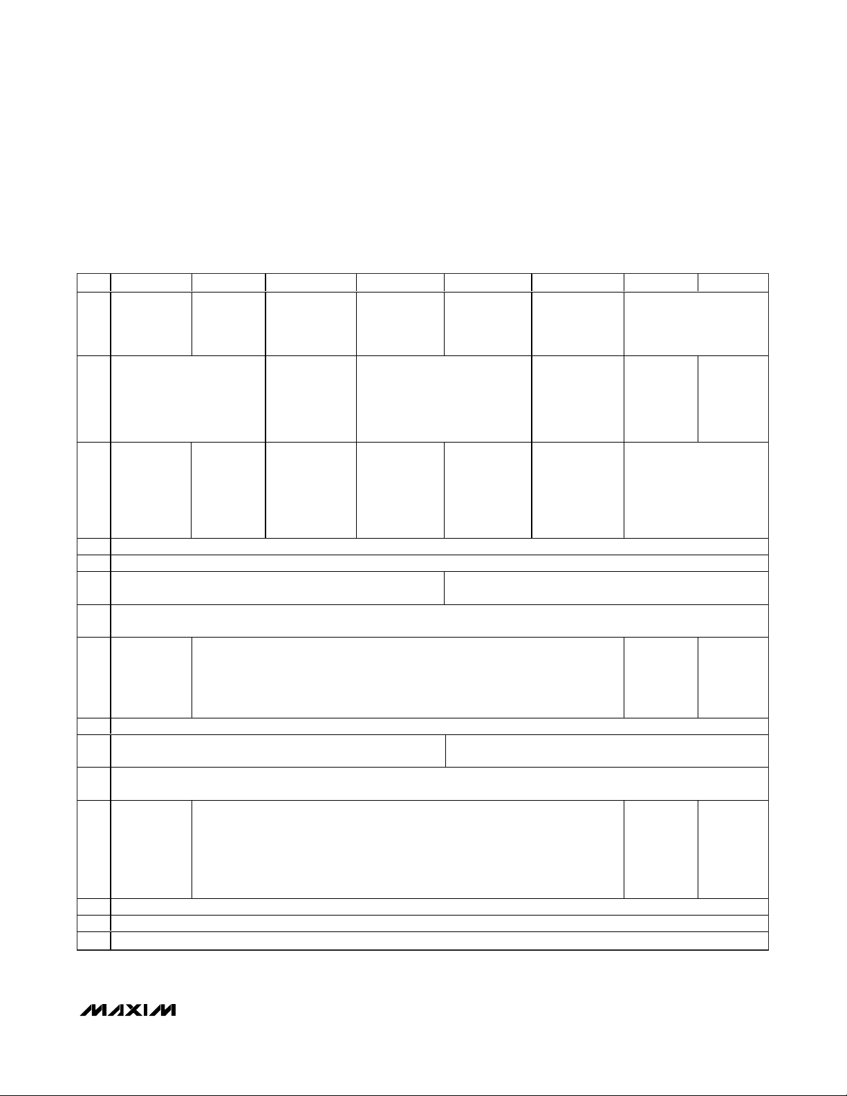
Programming Registers
Programming its registers with the SPI serial interface
sets the MAX5894 operation modes. Table 2 shows all
of the registers. The following are descriptions of each
register.
14-Bit, 500Msps, Interpolating and Modulating
Dual DAC with CMOS Inputs
______________________________________________________________________________________ 15
Table 2. MAX5894 Programmable Registers
Conditions in bold are default states after reset.
ADD BIT 7 BIT 6 BIT 5 BIT 4 BIT 3 BIT 2 BIT 1 BIT 0
00h Unused
Interpolation Rate
(Bit 7, Bit 6)
00 = No interpolation
01h
01 = 2x interpolation
10 = 4x interpolation
11 = 8x interpolation
0 = Two’s
complement
input data
02h
1 = Offset
binary input
data
03h Unused
04h 8-Bit IDAC Fine-Gain Adjustment (see the Gain Adjustment section). Bit 7 is MSB and bit 0 is LSB. Default: 00h
05h Unused
10-Bit IDAC Offset Adjustment (see the Offset Adjustment section). Bits 7 to 0 of the 06h register are the MSB bits. Bit 1 and bit 0 are the LSB
06h
bits in 07h register. Default: 000h
IDAC IOFFSET
Direction
0 = Current on
07h
OUTIN
1 = Current on
OUTIP
08h 8-Bit QDAC Fine-Gain Adjustment (see the Gain Adjustment section). Bit 7 is MSB and bit 0 is LSB. Default: 00h
09h Unused
10-Bit QDAC Offset Adjustment (see the Offset Adjustment section). Bits 7 to 0 of the 0Ah register are the MSB bits. Bit 1 and bit 0 are the
0Ah
LSB bits in 0Bh register. Default: 000h
QDAC
IOFFSET
Direction
0 = Current on
0Bh
OUTQN
1 = Current on
OUTQP
0Ch Reserved, do not write to these bits.
0Dh Reserved, do not write to these bits.
0Eh Reserved, do not write to these bits.
0 = MSB first
1 = LSB first
0 = Single
port (A),
interleaved
I/Q
1 = Dual port
I/Q input
Unused
Unused
Software Reset
0 = Normal
1 = Reset all
registers
Third
Interpolation
Filter
Configuration
0 = Lowpass
1 = Highpass
0 = Clock output
on DATACLK
1 = Clock output
on D ATAC LK/B12
Interpolator
Power-Down
0 = Normal
1 = Power-down
Modulation Mode
(Bit 4, Bit 3)
00 = Modulation off
/2
01 = f
IM
/4
10 = f
IM
11 = f
/4
IM
0 = Input data
latched on
rising clock
edge
1 = Input data
latched on falling
clock edge
IDAC PowerDown
0 = Normal
1 = Power-down
0 = Data clock
input enabled
1 = Data clock
output enabled
4-Bit IDAC Coarse-Gain Adjustment (see the Gain Adjustment
section). Bit 3 is MSB and bit 0 is LSB. Default: Fh
4-Bit QDAC Coarse-Gain Adjustment (see the Gain Adjustment
section). Bit 3 is MSB and bit 0 is LSB. Default: Fh
QDAC PowerDown
0 = Normal
1 = Power-down
Mixer Modulation
Mode
0 = Complex
1 = Real
Data
Synchronizer
0 = Enabled
1 = Disabled
Unused
Modulation
Sign
-jω
0 = e
-jω
1 = e
Unused
IDAC Offset
Adjustment
Bit 1
(see 06h
register)
QDAC Offset
Adjustment
Bit 1
(see 0Ah
register)
Unused
IDAC Offset
Adjustment
Bit 0
(see 06h
register)
QDAC Offset
Adjustment
Bit 0
(see 0Ah
register)
Page 16

MAX5894
14-Bit, 500Msps, Interpolating and Modulating
Dual DAC with CMOS Inputs
16 ______________________________________________________________________________________
Address 00h
Bit 6 Logic 0 (default) causes the serial port to use
MSB first address/data format. When set to a
logic 1, the serial port uses LSB first address/
data format.
Bit 5 When set to a logic 1, all registers reset to
their default state (this bit included).
Bit 4 Logic 1 stops the clock to the digital interpo-
lators. DAC outputs hold last value prior to
interpolator power-down.
Bit 3 IDAC power-down mode. A logic 1 to this bit
powers down the IDAC.
Bit 2 QDAC power-down mode. A logic 1 to this bit
powers down the QDAC.
Note: If both bit 2 and bit 3 are 1, the MAX5894 is in
full-power-down mode, leaving only the serial interface
active.
Address 01h
Bits 7, 6 Configure the interpolation filters according
to the following table:
00 1x (no interpolation)
01 2x
10 4x
11 8x (default)
Bit 5 Logic 0 configures FIR3 as a lowpass digital
filter (default). A logic 1 configures FIR3 as a
highpass digital filter.
Bits 4, 3 Configure the modulation frequency accord-
ing to the following table:
00 No modulation
01 fIM/2 modulation
10 fIM/4 modulation (default)
11 fIM/4 modulation
where fIMis the data rate at the input of the
modulator.
Bit 2 Configures the modulation mode for either
real or complex (image reject) modulation.
Logic 1 sets the modulator to the real mode
(default). Complex modulation is only available for f
IM
/4 modulation.
Bit 1 Quadrature modulator sign inversion. With I-
channel data leading Q-channel data by 90°,
logic 0 sets the complex modulation to be
e
-jw
(default), cancelling the upper image
when used with an external quadrature modulator. A logic 1 sets the complex modulation
to be e
+jw
, cancelling the lower image when
used with an external quadrature modulator.
Address 02h
Bit 7 Logic 0 (default) configures the data port for
two’s complement. A logic 1 configures the
data ports for offset binary.
Bit 6 Logic 0 (default) configures the data bus for
single-port, interleaved I/Q data. I and Q data
enter through one 14-bit bus. Logic 1 configures the data bus for dual-port I/Q data. I and
Q data enter on separate buses.
Bit 5 Logic 0 (default) configures the data clock
for pin 14. A logic 1 configures the data clock
for pin 27 (DATACLK/B12).
Bit 4 Logic 0 (default) sets the internal latches to
latch the data on the rising edge of DATACLK.
A logic 1 sets the internal latches to latch the
data on the falling edge of DATACLK.
Bit 3 Logic 0 (default) configures the DATACLK
pin (pin 14 or pin 27) to be an input. A logic 1
configures the DATACLK pin to be an output.
Bit 2 Logic 0 (default) enables the data synchro-
nizer circuitry. A logic 1 disables the data
synchronizer circuitry.
Address 03h
Bits 7–0 Unused.
Address 04h
Bits 7–0 These 8 bits define the binary number for
fine-gain adjustment of the IDAC full-scale
current (see the
Gain Adjustment
section). Bit
7 is the MSB. Default is all zeros.
Address 05h
Bits 3–0 These four bits define the binary number for
the coarse-gain adjustment of the IDAC fullscale current (see the
Gain Adjustment
sec-
tion). Bit 3 is the MSB. Default is all ones.
Address 06h, Bits 7–0; Address 07h, Bit 1 and Bit 0
These 10 bits represent a binary number that
defines the magnitude of the offset added to
the IDAC output (see the
Offset Adjustment
section). Default is all zeros.
Page 17
Address 07h
Bit 7 Logic 0 (default) adds the 10 bits offset cur-
rent to OUTIN. A logic 1 adds the 10 bits offset current to OUTIP.
Address 08h
Bits 7–0 These eight bits define the binary number for
fine-gain adjustment of the QDAC full-scale
current (see the
Gain Adjustment
section). Bit
7 is the MSB. Default is all zeros.
Address 09h
Bits 3–0 These four bits define the binary number for
the coarse-gain adjustment of the QDAC fullscale current (see the
Gain Adjustment
sec-
tion). Bit 3 is the MSB. Default is all ones.
Address 0Ah, Bits 7–0; Address 0Bh, Bit 1 and Bit 0
These 10 bits represent a binary number that
defines the magnitude of the offset added to
the QDAC output (see the
Offset Adjustment
section). Default is all zeros.
Address 0Bh
Bit 7 Logic 0 (default) adds the 10 bits offset to
OUTQN. A logic 1 adds the 10 bits offset to
OUTQP.
Offset Adjustment
Offset adjustment is achieved by adding a digital code to
the DAC inputs. The code OFFSET (see equation below),
as stored in the relevant control registers, has a range
from 0 to 1023 and a sign bit. The applied DAC offset is
stored in the register, providing an offset adjustment
range of ±1023 LSB codes. The resolution is 1 LSB.
Gain Adjustment
Gain adustment is peformed by varying the full-scale
current according to the following formula:
where I
REF
is the reference current (see the
Reference
Input/Output
section). COARSE is the register content
of registers 05h and 09h for the I- and Q-channel,
respectively. FINE is the register content of register 04h
and 08h for the I- and Q-channel, respectively. The
range of coarse is from 0 to 15, with 15 being the
default. The range for FINE is from 0 to 255 with 0
being the default. The gain can be adjusted in steps of
approximately 0.01dB.
Single-Port/Dual-Port Data-Input Modes
The MAX5894 is capable of capturing data in singleport and dual-port modes (selected through bit 6,
address 02h). In single-port mode, the data for both
DAC channels is latched on the A port (A13–A0).
The channel for the input data is determined by the
state of the SELIQ/B13 (pin 26) bit. When SELIQ is set
to logic-high, the input data is presented to the
I-channel, when set to logic-low, the input data is
presented to the Q-channel. The unused B-port inputs
(DATACLK/B12, B11–B0) should be grounded when
running in single-port mode.
Dual-port mode, as the name implies, requires that
each channel receives its data from a separate data
bus. SELIQ/B13 and DATACLK/B12 revert to data bit
inputs for the Q-channel in dual-port mode.
The MAX5894 control registers can be programmed to
allow either signed or unsigned binary format (bit 7,
address 02h) data in either single-port or dual-port
mode. Table 3 shows the corresponding DAC output
levels when using signed or unsigned data modes.
Data Synchronization Modes
Data synchronization circuitry is provided to allow operation with an input data clock. The data clock must be
frequency locked to the DAC clock (f
DAC
), but can
have arbitrary phase with respect to the DAC clock.
The synchronization circuitry allows for phase jitter on
the input data clock of up to ±1 data clock cycles.
Synchronization is initially established when the reset
pin is asynchronously deasserted and the input data
clock has been running for at least four clock cycles.
Subsequently, the MAX5894 monitors the phase rela-
MAX5894
14-Bit, 500Msps, Interpolating and Modulating
Dual DAC with CMOS Inputs
______________________________________________________________________________________ 17
Table 3. DAC Output Code Table
I
OFFSET OUTFS
OFFSET
=×
2
14
I
DIGITAL INPUT CODE
OFFSET
BINARY
(UNSIGNED)
00 0000 0000 0000 10 0000 0000 0000 0 I
01 1111 1111 1111 00 0000 0000 0000 I
11 1111 1111 1111 01 1111 1111 1111 I
TWO'S
COMPLEMENT
(SIGNED)
OUT_P OUT_N
OUTFS
/2 I
OUTFS
OUTFS
OUTFS
0
/2
⎡
⎢
⎣
I
OUTFS
I
×
3
⎛
⎜
⎝
⎞
COARSE
⎛
REF REF
⎜
⎟
⎝
⎠
4
16
+
1
⎞
⎟
⎠
3
⎛
−
⎜
⎝
I
×
32 256
⎞
⎟
⎠
FINE
⎛
⎜
⎝
⎤
1024
⎞
⎛
=
⎟
⎜
⎥
⎠
⎝
24
⎦
⎞
⎟
⎠
Page 18
MAX5894
tionship and detects if the phase drifts more than ±1
data clock cycle. If this occurs, the synchronizer automatically re-establishes synchronization. However, during the resynchronization phase, up to 8 data words
may be lost or repeated.
Bit 2 of register 02h disables or enables (default) the
automatic data clock phase detection. Disabling the
data synchronization circuitry requires the data clock
and the DAC clock phase to be locked.
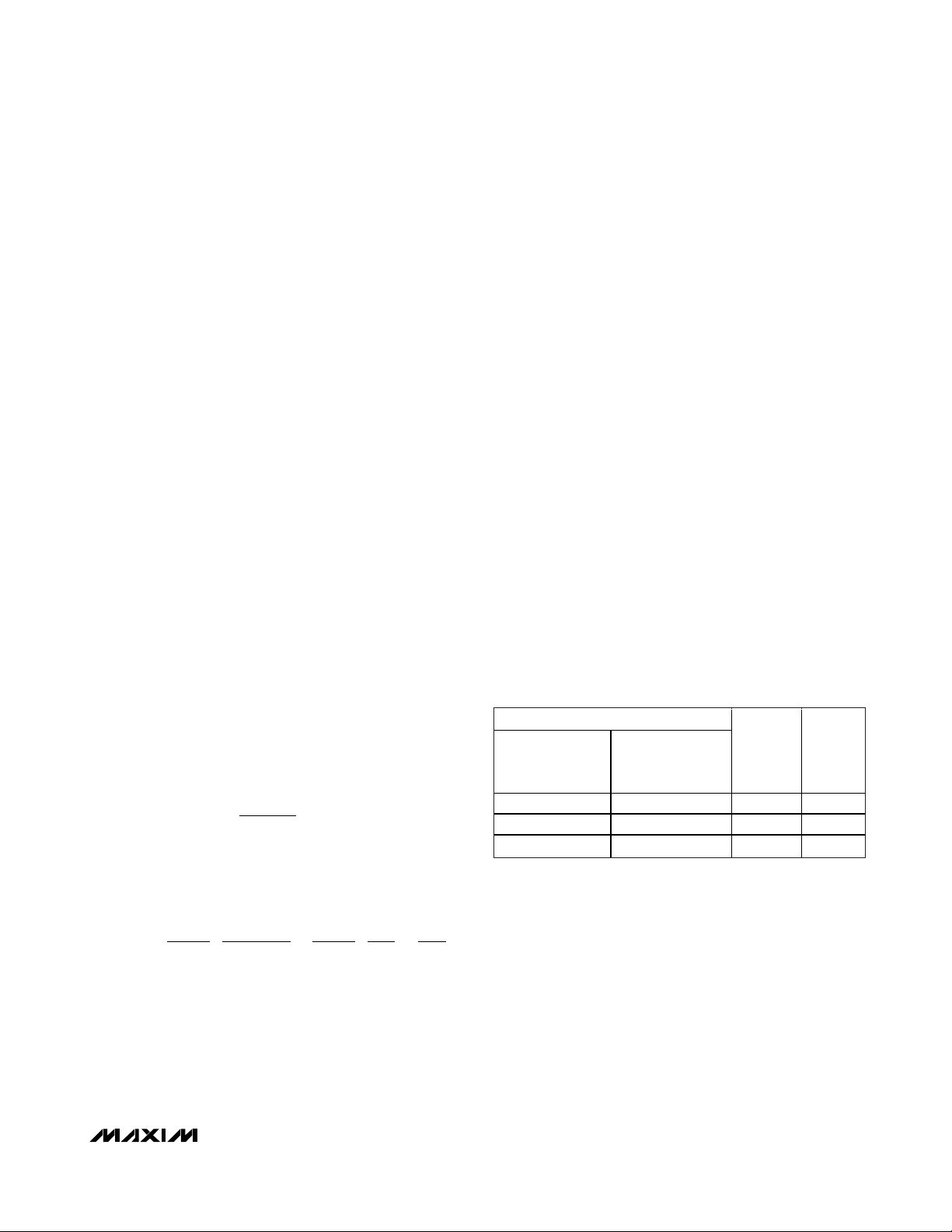
DATACLK Modes
The MAX5894 has a main DATACLK available at
pin 14. An alternate DATACLK is available at pin 27
(DATACLK/B12) when configured in single-port data
input mode (bit 5, address 02h). The DATACLK can be
configured to accept an input clock signal for latching
the input data, or to source a clock signal that can drive
up to 10pF load while latching the input data (bit 3,
address 02h). If DATACLK is configured as an output, it
is frequency divided from the CLKP/CLKN input,
depending on the operating mode, see Table 4.
The MAX5894 can be configured to latch the input
data on either the rising edge or falling edge of the
DATACLK signal (bit 4, address 02h). Figure 4 shows
the timing requirements between the DATACLK signal
and the input-data bus with latching on the rising edge.
14-Bit, 500Msps, Interpolating and Modulating
Dual DAC with CMOS Inputs
18 ______________________________________________________________________________________
Table 4. Clock Frequency Ratios in
Various Modes
Figure 4. Data-Input Timing Diagram
CLKP–CLKN
INPUT
MODE
Single
Port
Dual Port
INTERPOLATION
RATE
1x 1:1 1:2
2x 1:1 1:1
4x 1:2 1:1
8x 1:4 1:1
1x 1:1 1:1
2x 1:2 1:1
4x 1:4 1:1
8x 1:8 1:1
f
DATA:fCLKfDAC:fCLK
DATACLK
A0–A13/B0–B13
t
CLK
t
D
t
DS
t
DH
Page 19

MAX5894
14-Bit, 500Msps, Interpolating and Modulating
Dual DAC with CMOS Inputs
______________________________________________________________________________________ 19
Interpolating Filter
The MAX5894 features three cascaded FIR half-band
filters. The interpolating filters are enabled or disabled
in combinations to support 1x (no interpolation), 2x, 4x,
or 8x interpolation. Bits 7 and 6 of register 01h set the
interpolation rate (see Table 2). The last interpolation fil-
ter is located after the modulator. In the 8x interpolation
mode, the last filter (FIR3) can be configured as lowpass or highpass (bit 5, address 01h) to select the
lower or upper sideband from the modulation output.
The frequency responses of these three filters are plotted in Figures 5–8.
Figure 5. Interpolation Filter Frequency Response, 2x
Interpolation Mode
Figure 6. Interpolation Filter Frequency Response, 4x
Interpolation Mode
Figure 7. Interpolation Filter Frequency Response, 8x
Interpolation Mode (FIR3 Lowpass Mode)
Figure 8. Interpolation Filter Frequency Response, 8x
Interpolation Mode (FIR3 Highpass Mode)
0
-20
-40
-60
GAIN (dBFS)
-80
-100
-120
0.2
0 0.4 0.6 0.8
f
OUT
-0.0002
-0.0004
- NORMALIZED TO INPUT DATA RATE
PASSBAND DETAIL
0
0.3
0.2
0.1
0
1.0 1.2 1.4 1.6 1.8 2.0
0.4
0
-20
-40
-60
-0.0002
-0.0004
GAIN (dBFS)
-80
-100
-120
0 1.0 1.5 2.0
0.5
- NORMALIZED TO INPUT DATA RATE
f
OUT
PASSBAND DETAIL
0
0.4
0.3
0
0.2
0.1
2.5 3.0 3.5 4.0
0
-20
PASSBAND DETAIL
-0.0002
-0.0004
0
0.4
0.3
0.2
0.1
0
-40
-60
GAIN (dBFS)
-80
-100
-120
1
0234
f
- NORMALIZED TO INPUT DATA RATE
OUT
5678
0
-20
-40
-60
GAIN (dBFS)
-0.0002
-0.0004
PASSBAND DETAIL
0
3.6 3.8 4.0 4.2 4.4
-80
-100
-120
1
0234
f
- NORMALIZED TO INPUT DATA RATE
OUT
5678
Page 20

MAX5894
The programmable interpolation filters multiply the
MAX5894 input data rate by a factor of 2x, 4x, or 8x to
separate the reconstructed waveform spectrum and the
DAC image. The original spectral images, appearing at
around multiples of the input data rate, are attenuated
by the internal digital filters. This feature provides three
benefits:
1) Image separation reduces complexity of analog
reconstruction filters.
2) Lower input data rates eliminate board-level highspeed data transmission.
3) Sin(x)/x rolloff is reduced over the effective bandwidth.
Figure 9 illustrates a practical example of the benefits
when using the MAX5894 in 2x, 4x, and 8x interpolation
modes with the third filter configured as a lowpass filter.
With no interpolation filter, the first image signal appears
in the second Nyquist zone between fS/2 and fS. The first
interpolating filter removes this image. In fact, all of the
14-Bit, 500Msps, Interpolating and Modulating
Dual DAC with CMOS Inputs
20 ______________________________________________________________________________________
Figure 9. Spectral Representation of Interpolating Filter Responses (Output Frequencies are Relative to the Data Input Frequency, fS)
FILTER
IMAGE
IMAGE
RESPONSE
3f
S
3f
S
3f
S
INPUT
SPECTRUM
AND FIRST
FILTER
RESPONSE
OUTPUT
SPECTRUM
OF THE
FIRST
FILTER
INPUT
SPECTRUM
AND
SECOND
FILTER
RESPONSE
SIGNAL
SIGNAL
SIGNAL
IMAGE
f
S
f
S
f
S
2f
S
2f
S
2f
S
NO INTERPOLATION
4f
S
4f
S
4f
S
5f
5f
5f
S
S
S
FILTER
RESPONSE
6f
S
6f
S
6f
S
7f
S
7f
S
7f
S
8f
S
2x INTERPOLATION
8f
S
8f
S
OUTPUT
SPECTRUM
OF THE
SECOND
FILTER
INPUT
SPECTRUM
AND THIRD
FILTER
RESPONSE
OUTPUT
SPECTRUM
OF THE
THIRD
FILTER
SIGNAL
SIGNAL
SIGNAL
IMAGE
f
S
f
S
f
S
2f
2f
2f
S
S
S
FILTER
RESPONSE
3f
S
3f
S
3f
S
4f
S
4f
S
4f
S
IMAGE
5f
S
5f
S
5f
S
6f
S
6f
S
6f
S
7f
S
7f
S
IMAGE
7f
S
4x INTERPOLATION
8f
S
8f
S
8x INTERPOLATION
8f
S
Page 21
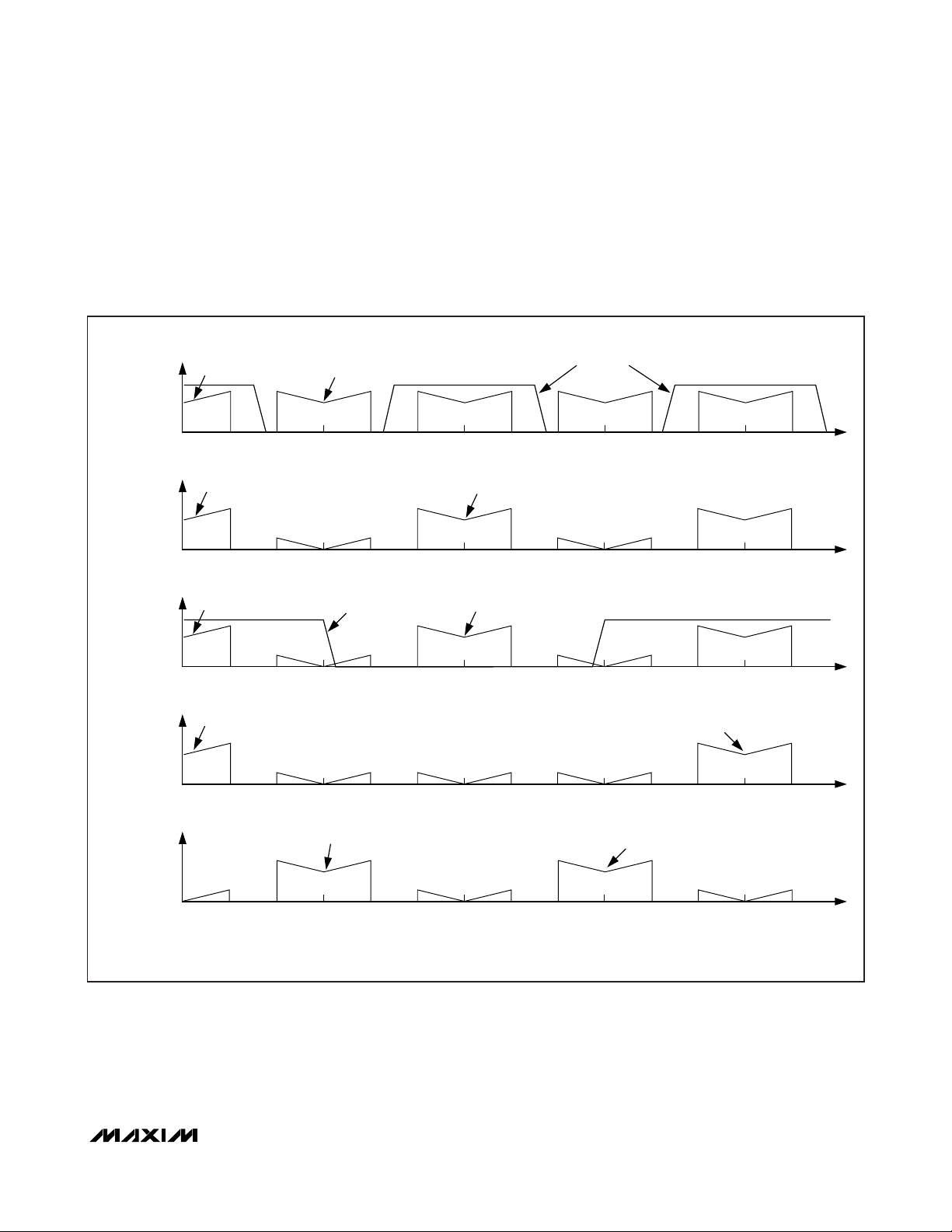
images at odd numbers of fSare filtered. At the output of
the first filter, the images are at 2fS, 4fS, etc. This signal is
then passed to the second interpolating filter, which is
similar to the first filter and removes the images at 2fS, 6fS,
10fS, etc. Finally, the third filter removes images at 4fS,
12fS, 20fS, etc. Figures 10, 11, and 12 similarly illustrate
the spectral responses when using the interpolating filters
combined with the digital modulator.
MAX5894
14-Bit, 500Msps, Interpolating and Modulating
Dual DAC with CMOS Inputs
______________________________________________________________________________________ 21
Figure 10. Spectral Representation of 4x Interpolation Filter with fIM/4 Modulation (Output Frequencies are Relative to the Data Input
Frequency, f
S
)
INPUT
SPECTRUM
AND FIRST
FILTER
RESPONSE
OUTPUT
SPECTRUM
OF THE
FIRST
FILTER
INPUT
SPECTRUM
AND
SECOND
FILTER
RESPONSE
SIGNAL
SIGNAL
SIGNAL
f
f
f
IMAGE
S
S
FILTER
RESPONSE
S
FILTER
RESPONSE
2f
S
IMAGE
2f
S
IMAGE
2f
S
3f
S
3f
S
3f
S
NO INTERPOLATION
4f
S
2x INTERPOLATION
4f
S
4f
S
OUTPUT
SPECTRUM
OF THE
SECOND
FILTER
OUTPUT
SPECTRUM
OF THE
MODULATOR
SIGNAL
f
S
SIGNAL
LOWER
SIDEBAND
FOR COMPLEX MODULATION THE MODULATION SIGN (BIT 1, ADDRESS 01h) SELECTS UPPER OR LOWER SIDEBAND
UPPER
SIDEBAND
f
S
2f
S
2f
S
3f
S
IMAGE
3f
S
IMAGE
4x INTERPOLATION
4f
S
4f
S
Page 22

MAX5894
14-Bit, 500Msps, Interpolating and Modulating
Dual DAC with CMOS Inputs
22 ______________________________________________________________________________________
Figure 11. Spectral Representation of 8x Interpolation Filter with fIM/4 Modulation and Lowpass Mode Enabled (Output Frequencies
are Relative to the Data Input Frequency, f
S
)
INPUT
SIGNAL
SPECTRUM
AND FIRST
FILTER
RESPONSE
OUTPUT
SPECTRUM
OF THE
FIRST
FILTER
INPUT
SPECTRUM
SIGNAL
AND
SECOND
FILTER
RESPONSE
OUTPUT
SIGNAL
SPECTRUM
OF THE
SECOND
FILTER
SIGNAL
FILTER
IMAGE
f
S
2f
S
RESPONSE
3f
S
4f
S
5f
S
6f
S
7f
S
IMAGE
f
S
2f
S
3f
S
4f
S
5f
S
6f
S
7f
S
NO INTERPOLATION
8f
S
2x INTERPOLATION
8f
S
FILTER
4f
S
4f
S
RESPONSE
IMAGE
5f
S
6f
S
7f
S
8f
S
4x INTERPOLATION
5f
S
6f
S
7f
S
8f
S
IMAGE
f
S
f
S
2f
S
2f
S
3f
S
3f
S
SIGNAL
OUTPUT
LOWER
SIDEBAND
UPPER
SIDEBAND
IMAGE
SPECTRUM
OF THE
MODULATOR
f
S
2f
S
3f
S
4f
S
5f
S
6f
S
7f
S
8f
S
FOR COMPLEX MODULATION THE MODULATION SIGN (BIT 1, ADDRESS 01h) SELECTS UPPER OR LOWER SIDEBAND
FILTER RESPONSE
IMAGE
INPUT
SPECTRUM
SIGNAL
AND THIRD
FILTER
RESPONSE
OUTPUT
SPECTRUM
f
S
SIGNAL
2f
S
3f
S
4f
S
5f
S
6f
S
IMAGE
7f
S
8f
S
8x INTERPOLATION
OF THE
THIRD
FILTER
f
S
2f
S
3f
S
4f
S
5f
S
6f
S
7f
S
8f
S
Page 23
MAX5894
14-Bit, 500Msps, Interpolating and Modulating
Dual DAC with CMOS Inputs
______________________________________________________________________________________ 23
Figure 12. Spectral Representation of 8x Interpolation Filter with fIM/4 Modulation and Highpass Mode Enabled (Output Frequencies
are Relative to the Data Input Frequency, f
S
)
INPUT
SPECTRUM
AND FIRST
FILTER
RESPONSE
SIGNAL
FILTER
IMAGE
f
S
2f
S
RESPONSE
3f
S
4f
S
5f
S
6f
S
7f
S
NO INTERPOLATION
8f
S
OUTPUT
SPECTRUM
OF THE
FIRST
FILTER
INPUT
SPECTRUM
AND
SECOND
FILTER
RESPONSE
OUTPUT
SPECTRUM
OF THE
SECOND
FILTER
OUTPUT
SPECTRUM
OF THE
MODULATOR
SIGNAL
SIGNAL
SIGNAL
f
S
f
S
f
S
IMAGE
2f
S
IMAGE
2f
S
3f
S
4f
S
5f
S
6f
S
FILTER
RESPONSE
3f
S
4f
S
5f
S
6f
S
IMAGE
2f
S
3f
S
4f
S
5f
S
6f
S
SIGNAL
LOWER
SIDEBAND
f
S
UPPER
SIDEBAND
IMAGE
2f
S
3f
S
4f
S
5f
S
6f
S
FOR COMPLEX MODULATION THE MODULATION SIGN (BIT 1, ADDRESS 01h) SELECTS UPPER OR LOWER SIDEBAND
2x INTERPOLATION
7f
S
7f
S
8f
S
8f
S
4x INTERPOLATION
7f
S
7f
S
8f
S
8f
S
INPUT
SPECTRUM
SIGNAL
IMAGE
FILTER
RESPONSE
AND THIRD
FILTER
RESPONSE
OUTPUT
SPECTRUM
f
S
2f
S
3f
S
SIGNAL
4f
S
5f
S
IMAGE
6f
S
7f
S
8f
S
8x INTERPOLATION
OF THE
THIRD
FILTER
f
S
2f
S
3f
S
4f
S
5f
S
6f
S
7f
S
8f
S
Page 24

MAX5894
Digital Modulator
The MAX5894 features digital modulation at frequencies
of fIM/2 and fIM/4, where fIMis the data rate at the input
to the modulator. fIMequals f
DAC
in 1x, 2x, and 4x inter-
polation modes. In 8x interpolation mode, f
IM
equals
f
DAC
/2. The output rate of the modulator is always the
same as the input data rate to the modulator.
In complex modulation mode, data from the second
interpolation filter is frequency mixed with the on-chip
in-phase and quadrature (I/Q) local oscillator (LO).
Complex modulation provides the benefit of image
sideband rejection when combined with an external
quadrature modulator commonly found in wireless
communication systems.
In the f
LO
= fIM/4 mode, real or complex modulation can
be used. The modulator multiplies successive input data
samples by the sequence [1, 0, -1, 0] for a cos(ωt). The
modulator modulates the input signal up to f
IM
/4, creat-
ing upper and lower images around fIM/4. The quadrature LO sin(ωt) is realized by delaying the cos(ωt)
sequence by one clock cycle. Using complex modulation, complex IF is generated. The complex IF combined
with an external quadrature modulator provides image
rejection. The sign of the LO can be changed to allow
the user to select whether the upper or the lower image
should be rejected (bit 1 of register 01h).
When fIM/2 is chosen as the LO frequency, the input
signal is multiplied by [-1, 1] on both channels. This produces images around fIM/2. The complex image-reject
modulation mode is not available for this LO frequency.
The outputs of the modulator can be expressed as:
in complex modulation, e
+jwt
in complex modulation, e
-jwt
where ω = 2 x π x fLO.
For real modulation, the outputs of the modulator can
be expressed as:
If more than one MAX5894 is used, their LO phases
can be synchronized by simultaneously releasing
RESET. This sets the MAX5894 to its predefined initial
phase.
Device Reset
The MAX5894 can be reset by holding the RESET pin
low for 10ns. This will program the control registers to
their default values in Table 2. During power-on, RESET
must be held low until all power supplies have stabilized. Alternatively, programming bit 5 of address 00h
to a logic-high also resets the MAX5894 after power-up.
14-Bit, 500Msps, Interpolating and Modulating
Dual DAC with CMOS Inputs
24 ______________________________________________________________________________________
Figure 13. (a) Modulator in Complex Modulation Mode; (b) Modulator in Real Modulation Mode
I-CHANNEL
INPUT DATA
It At t Bt t
()=()×() ()×()
=
Qt At t Bt t
()
sin cos
()×()+()×()
It At t Bt t
()=()×()+()×()
Qt At t Bt t
cos sin
=
sin cos
()×()+()×()
()
− cos sin
ωω
ωω
ωω
ωω
It At t
()=()×()
Qt At t
cos
=
cosωω
()×()
()
I-CHANNEL
INPUT DATA
cos(ωt)
sin(ωt)
sin(ωt)
Q-CHANNEL
INPUT DATA
cos(ωt)
(a)
∑
∑
I-CHANNEL
OUTPUT DATA
TO
FIR3
Q-CHANNEL
OUTPUT DATA
Q-CHANNEL
INPUT DATA
cos(ωt)
sin(ωt)
sin(ωt)
cos(ωt)
(b)
∑
∑
I-CHANNEL
OUTPUT DATA
TO
FIR3
Q-CHANNEL
OUTPUT DATA
Page 25

Power-Down Mode
The MAX5894 features three power-saving modes.
Each DAC can be individually powered down through
bits 2 and 3 of address 00h. The interpolation filters can
also be powered down through bit 4 of address 00h,
preserving the output level of each DAC (the DACs
remain powered). Powering down both DACs automatically puts the MAX5894 into full power-down, including
the interpolation filters.
Applications Information
Frequency Planning
System designers need to take the DAC into account
during frequency planning for high-performance applications. Proper frequency planning can ensure that
optimal system performance is achieved. The
MAX5894 is designed to deliver excellent dynamic performance across wide bandwidths, as required for
communication systems. As with all DACs, some combinations of output frequency and update rate produce
better performance than others.
Harmonics are often folded down into the band of interest. Specifically, if the DAC outputs a frequency close
to fS/N, the Mth harmonic of the output signal will be
aliased down to:
Thus, if N ≈ (M + 1), the Mth harmonic will be close to
the output frequency. SFDR performance of a currentsteering DAC is often dominated by 3rd-order harmonic
distortion. If this is a concern, placing the output signal
at a different frequency other than fS/4 should be considered.
Common to interpolating DACs are images near the
divided clocks. In a DAC configured for 4x interpolation,
this applies to images around fS/4 and fS/2. In a DAC
configured for 8x interpolation, this applies to images
around fS/8, fS/4, and fS/2. Most of these images are
not part of the in-band (0 to f
DATA
/2) SFDR specification, though they are a consideration for out-of-band
(f
DATA
/2 - f
DAC
/2) SFDR and may depend on the rela-
tionship of the DATACLK to DAC update clock (see the
Data Clock
section). When specifying the output reconstruction filter for other than baseband signals, these
images should not be ignored.
Data Clock
The MAX5894 features synchronizers that allow for arbitrary phase alignment between DATACLK and
CLKP/CLKN. The DATACLK causes internal switching in
the MAX5894 and the phase between DATACLK (input
mode) to CLKP/CLKN influences the images at
DATACLK. Optimum image rejection is achieved when
DATACLK transitions are aligned with the falling edge of
CLKP. Figure 14 shows the image level near DATACLK
as a function of the DATACLK (input mode) to
CLKP/CLKN phase at 500Msps, 4x interpolation for a
10MHz, -6dBFS output signal.
Clock Interface
The MAX5894 features a flexible differential clock input
(CLKP, CLKN) with a separate supply (AV
CLK
) to
achieve optimum jitter performance. It uses an ultra-low
jitter clock to achieve the required noise density. Clock
jitter must be less than 0.5ps
RMS
to meet the specified
noise density. For that reason, the CLKP/CLKN input
source must be designed carefully. The differential
clock (CLKN and CLKP) input can be driven from a single-ended or a differential clock source. Differential
clock drive is required to achieve the best dynamic
performance from the DAC. For single-ended operation, drive CLKP with a low noise source and bypass
CLKN to GND with a 0.1µF capacitor.
The CLKP and CLKN pins are internally biased to
AV
CLK
/2. This allows the user to AC-couple clock
MAX5894
14-Bit, 500Msps, Interpolating and Modulating
Dual DAC with CMOS Inputs
______________________________________________________________________________________ 25
Figure 14. Effect of CLKP/CLKN to DATACLK Phase on fS/4
Images
ff Mf f
=×=
−
S OUT S
−
NM
⎡
⎤
⎢
⎥
N
⎣
⎦
fS/4 IMAGES vs. CLKP/CLKN to DATACLK DELAY
= 125Mwps, 4x INTERPOLATION
f
DATA
-50
-60
-70
-80
IMAGE LEVEL (dBc)
-90
-100
-110
08
fS/4 - f
OUT
fS/4 + f
OUT
CLKP/CLKN DELAY (ns)
f
A
OUT
OUT
= 10MHz
= -6dBFS
642
Page 26
MAX5894
sources directly to the device without external resistors
to define the DC level. The input resistance of CLKP
and CLKN is 5kΩ.
A convenient way to apply a differential signal is with a
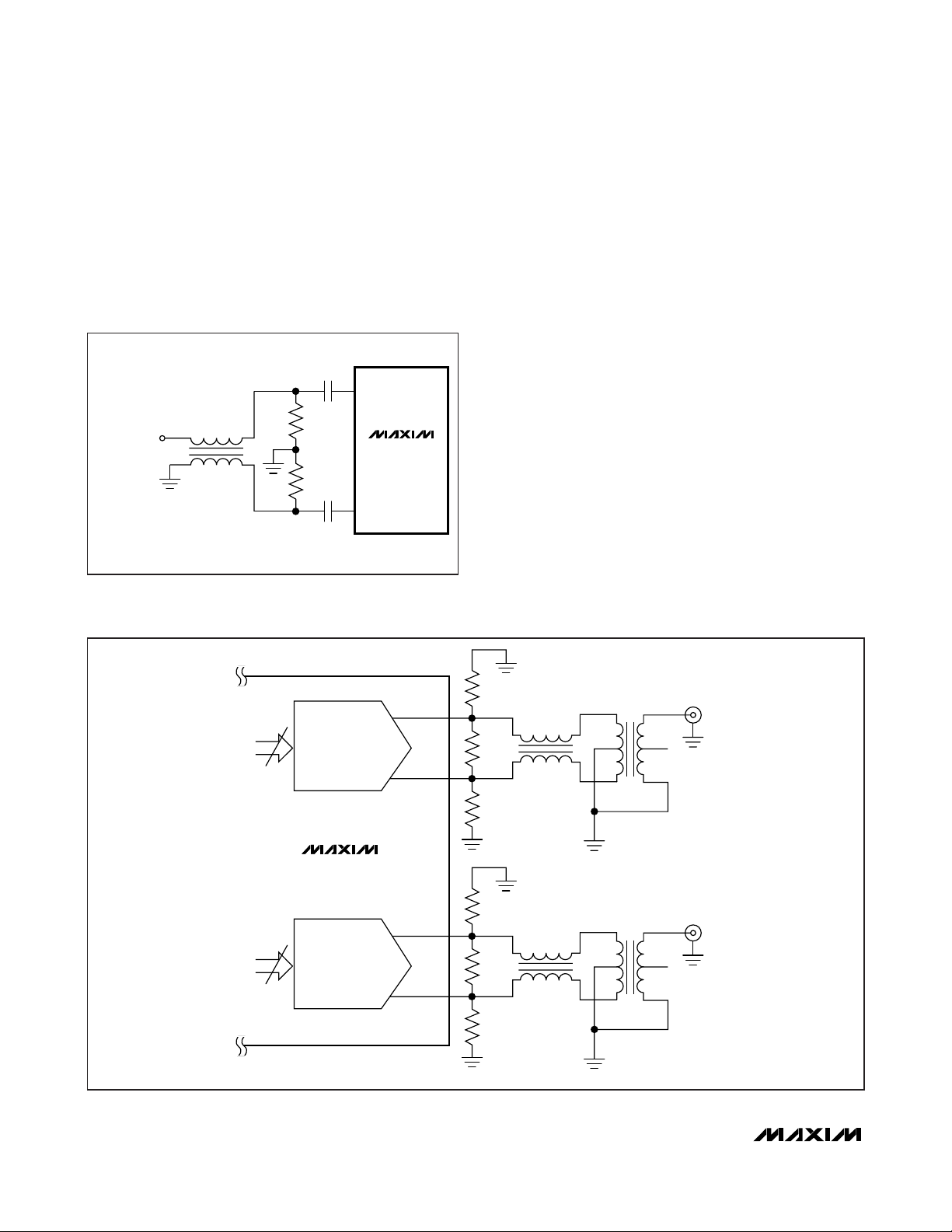
balun transformer as shown in Figure 15. Alternatively,
these inputs may be driven from a CMOS-compatible
clock source, however it is recommended to use
sine-wave or AC-coupled differential ECL/PECL drive for
best dynamic performance.
Output Interface (OUTI, OUTQ)
The MAX5894 outputs complementary currents (OUTIP,
OUTIN, OUTQP, and OUTQN) that can be utilized in a
differential configuration. Load resistors convert these
two output currents into a differential output voltage.
The differential output between OUTIP (OUTQP) and
OUTIN (OUTQN) can be converted to a single-ended
output using a transformer or a differential amplifier.
Figure 16 shows a typical transformer-based application circuit for generation of IF output signals. In this
configuration, the MAX5894 operates in differential
mode, which reduces even-order harmonics, and
increases the available output power. Pay close attention to the transformer core saturation characteristics
when selecting a transformer. Transformer core saturation can introduce strong second harmonic distortion,
especially at low output frequencies and high signal
amplitudes. It is recommended to connect the transformer center tap to ground.
14-Bit, 500Msps, Interpolating and Modulating
Dual DAC with CMOS Inputs
26 ______________________________________________________________________________________
Figure 15. Single-Ended-to-Differential Clock Conversion Using
a Balun Transformer
Figure 16. Differential-to-Single-Ended Conversion Using Wideband RF Transformers
MINI-CIRCUITS
SINGLE-ENDED
IINPUT
ADTL1-12
1:1 RATIO
100nF
CLKP
24.9Ω
MAX5894
24.9Ω
100nF
CLKN
50Ω
OUTIP
IDAC
14
OUTIN
MAX5894
OUTQP
QDAC
14
OUTQN
100Ω
1:1
50Ω
50Ω
100Ω
1:1
50Ω
, SINGLE-ENDED
V
IOUT
1:1
V
, SINGLE-ENDED
QOUT
1:1
Page 27
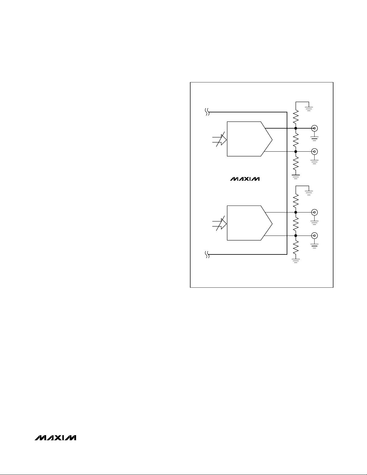
If a transformer is not used, the outputs must have a
resistive termination to ground. Figure 17 shows the
MAX5894 output configured for differential DC-coupled
mode. The DC-coupled configuration can be used to
eliminate waveform distortion due to highpass filter
effects. Applications include communication systems
employing analog quadrature upconverters and requiring a high-speed DAC for baseband I/Q synthesis.
If a single-ended DC-coupled unipolar output is desirable, OUTIP (OUTQP) should be selected as the output, and connect OUTIN (OUTQN) to ground. Using the
MAX5894 output single-ended is not recommended
because it introduces additional noise and distortion.
The distortion performance of the DAC also depends
on the load impedance. The MAX5894 is optimized for
a 50Ω double termination. It can be used with a transformer output as shown in Figure 16 or just one 25Ω
resistor from each output to ground and one 50Ω resistor between the outputs (Figure 17). Higher output termination resistors can be used, as long as each output
voltage does not exceed +1V with respect to GND, but
at the cost of degraded distortion performance and
increased output noise voltage.
Reference Input/Output
The MAX5894 supports operation with the on-chip 1.2V
bandgap reference or an external reference voltage
source. REFIO serves as the input for an external, lowimpedance reference source, and as the output if the
DAC is operating with the internal reference.
For stable operation with the internal reference, REFIO
should be decoupled to GND with a 1µF capacitor.
MAX5894
14-Bit, 500Msps, Interpolating and Modulating
Dual DAC with CMOS Inputs
______________________________________________________________________________________ 27
Figure 17. The DC-Coupled Differential Output Configuration
25Ω
OUTIP
IDAC
14
OUTIN
MAX5894
OUTQP
QDAC
14
OUTQN
50Ω
25Ω
25Ω
50Ω
25Ω
Page 28
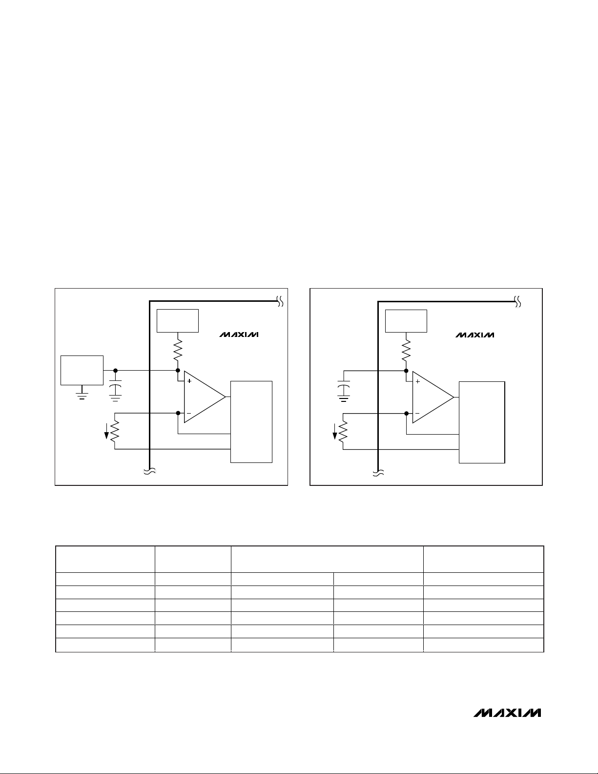
MAX5894
REFIO must be buffered with an external amplifier, if heavy
loading is required, due to its 10kΩ output resistance.
Alternatively, apply a temperature-stable external reference to REFIO (Figure 18). The internal reference is overdriven by the external reference. For improved accuracy
and drift performance, choose a fixed output voltage reference such as the MAX6520 bandgap reference.
The MAX5894’s reference circuit (Figure 19) employs a
control amplifier, designed to regulate the full-scale cur-
rent I
OUT
for the differential current outputs of the DAC.
The output current can be calculated as:
I
OUTFS
= 32 x I
REF
x 16383/16384
where I
REF
is the reference output current (I
REF
= V
REFIO
/
R
SET
). Located between FSADJ and DACREF, R
SET
is the
reference resistor, which determines the amplifier’s output
current for the DAC. Use Table 5 for a matrix of different
I
OUTFS
and R
SET
selections.
14-Bit, 500Msps, Interpolating and Modulating
Dual DAC with CMOS Inputs
28 ______________________________________________________________________________________
Figure 18. Typical External Reference Circuit
Figure 19. MAX5894 Internal Reference Architecture
Table 5. I
OUTFS
and R
SET
Selection Matrix Based on a Typical 1.20V Reference Voltage
*
Terminated into a 50Ωload.
1.2V
REFERENCE
MAX5894
CURRENT-
SOURCE
ARRAY DAC
EXTERNAL
1.25V
REFERENCE
10kΩ
REFIO
1µF
FSADJ
I
REF
R
SET
DACREF
1µF
I
REF
FSADJ
R
SET
DACREF
REFIO
1.2V
REFERENCE
10kΩ
MAX5894
CURRENT-
SOURCE
ARRAY DAC
FULL-SCALE
CURRENT
I
OUTFS
2 62.50 19.2 19.1 100
5 156.26 7.68 7.5 250
10 312.50 3.84 3.83 500
15 468.75 2.56 2.55 750
20 625.00 1.92 1.91 1000
(mA) I
REFERENCE
CURRENT
(µA) CALCULATED 1% EIA STD V
REF
(kΩ) OUTPUT VOLTAGE
R
SET
IOUTP/N
* (mV
P-P
)
Page 29

MAX5894
14-Bit, 500Msps, Interpolating and Modulating
Dual DAC with CMOS Inputs
______________________________________________________________________________________ 29
Power Supplies, Bypassing,
Decoupling, and Layout
Grounding and power-supply decoupling strongly influence the MAX5894 performance. Unwanted digital
crosstalk can couple through the input, reference,
power-supply, and ground connections, which can
affect dynamic specifications like signal-to-noise ratio
or spurious-free dynamic range. In addition, electromagnetic interference (EMI) can either couple into or
be generated by the MAX5894. Observe the grounding
and power-supply decoupling guidelines for highspeed, high-frequency applications. Follow the powersupply and filter configuration guidelines to achieve
optimum dynamic performance.
Using a multilayer PCB with separate ground and
power-supply planes, run high-speed signals on lines
directly above the ground plane. Since the MAX5894
has separate analog and digital sections, the PCB
should include separate analog and digital ground sections with only one point connecting the three planes at
the exposed pad under the MAX5894. Run digital signals above the digital ground plane and analog/clock
signals above the analog/clock ground plane. Keep
digital signals as far away from sensitive analog inputs,
reference lines, and clock inputs as practical. Use a
symmetric design of clock input and the analog output
lines to minimize 2nd-order harmonic distortion components, thus optimizing the dynamic performance of the
DAC. Keep digital signal paths short and run lengths
matched to avoid propagation delay and data skew
mismatches.
The MAX5894 requires five separate power-supply
inputs for the analog (AV
DD1.8
and AV
DD3.3
), digital
(DV
DD1.8
and DV
DD3.3
), and clock (AV
CLK
) circuitry.
Decouple each voltage supply pin with a separate
0.1µF capacitor as close to the device as possible and
with the shortest possible connection to the appropriate
ground plane. Minimize the analog and digital load
capacitances for optimized operation. Decouple all
power-supply voltages at the point they enter the PCB
with tantalum or electrolytic capacitors. Ferrite beads
with additional decoupling capacitors forming a pi-network could also improve performance.
The exposed pad MUST be soldered to the ground.
Use multiple vias, an array of at least 4 x 4 vias, directly
under the EP to provide a low thermal and electrical
impedance path for the IC.
Static Performance Parameter
Definitions
Integral Nonlinearity (INL)
Integral nonlinearity is the deviation of the values on an
actual transfer function from either a best straight-line fit
(closest approximation to the actual transfer curve) or a
line drawn between the end points of the transfer function, once offset and gain errors have been nullified.
For a DAC, the deviations are measured at every individual step.
Differential Nonlinearity (DNL)
Differential nonlinearity is the difference between an
actual step height and the ideal value of 1 LSB. A DNL
error specification of less than 1 LSB guarantees no
missing codes and a monotonic transfer function.
Offset Error
The offset error is the difference between the ideal and
the actual offset current. For a DAC, the offset point is
the average value at the output for the two midscale
digital input codes with respect to the full-scale of the
DAC. This error affects all codes by the same amount.
Gain Error
A gain error is the difference between the ideal and the
actual full-scale output voltage on the transfer curve,
after nullifying the offset error. This error alters the slope
of the transfer function and corresponds to the same
percentage error in each step.
Dynamic Performance
Parameter Definitions
Settling Time
The settling time is the amount of time required from the
start of a transition until the DAC output settles its new
output value to within the specified accuracy.
Noise Spectral Density
The DAC output noise is the sum of the quantization
noise and thermal noise. Noise spectral density is the
noise power in 1Hz bandwidth, specified in dBFS/Hz.
Signal-to-Noise Ratio (SNR)
For a waveform perfectly reconstructed from digital
samples, the theoretical maximum SNR is the ratio of
the full-scale analog output (RMS value) to the RMS
quantization error (residual error). The ideal, theoretical
maximum SNR can be derived from the DAC’s resolution (N bits):
SNR
dB
= 6.02dBx N + 1.76
dB
Page 30

MAX5894
However, noise sources such as thermal noise, reference noise, clock jitter, etc., affect the ideal reading.
Therefore, SNR is computed by taking the ratio of the
RMS signal to the RMS noise, which includes all spectral components minus the fundamental, the first four
harmonics, and the DC offset.
Spurious-Free Dynamic Range (SFDR)
SFDR is the ratio of the RMS amplitude of the carrier
frequency (maximum signal components) to the RMS
value of their next largest distortion component. SFDR
is usually measured in dBc and with respect to the carrier frequency amplitude or in dBFS with respect to the
DAC’s full-scale range. Depending on its test condition,
SFDR is observed within a predefined window or
to Nyquist.
Two-/Four-Tone Intermodulation
Distortion (IMD)
The two-tone IMD is the ratio expressed in dBc (or
dBFS) of the worst 3rd-order (or higher) IMD products
to either output tone.
Adjacent Channel Leakage
Power Ratio (ACLR)
Commonly used in combination with WCDMA (wideband code-division multiple-access), ACLR reflects the
leakage power ratio in dB between the measured powers within a channel relative to its adjacent channel.
ACLR provides a quantifiable method of determining
out-of-band spectral energy and its influence on an
adjacent channel when a bandwidth-limited RF signal
passes through a nonlinear device.
14-Bit, 500Msps, Interpolating and Modulating
Dual DAC with CMOS Inputs
30 ______________________________________________________________________________________
Page 31

MAX5894
14-Bit, 500Msps, Interpolating and Modulating
Dual DAC with CMOS Inputs
______________________________________________________________________________________ 31
Pin Configuration
PACKAGE TYPE PACKAGE CODE DOCUMENT NO.
68 QFN-EP G6800-4
21-0122
Package Information
For the latest package outline information and land patterns, go to www.maxim-ic.com/packages.
CLKP
CLKN
N.C.
N.C.
N.C.
D
VDD1.8
A13
A12
A11
A10
D
VDD3.3
DATACLK
TOP VIEW
10
A9
11
A8
12
13
14
A7
15
A6
16
A5 17
DD1.8
CLK
AV
68
1
2
3
4
5
6
7
8
9
EXPOSED PAD
DD3.3
GND
GND
AV
OUTIP
64
656667
AV
OUTIN
GND
MAX5894
DD3.3
AV
GND
OUTQP
5859606162 5455565763
OUTQN
GND
DD3.3
AV
GND
DD1.8
AV
5253
FSADJ
51
50
49
48 CS
47
46
45
44
43
42
41
40
39
38
37 DV
36
35
DACREF
REFIO
RESET
SCLK
DIN
DOUT
DV
DD3.3
N.C.
N.C.
B0
B1
B2
B3
DD1.8
B4
B5
2322212019 2726252418 2928 323130
A3
A2
A4
DD1.8
DV
A0
A1
N.C.
N.C.
B11
SELIQ/B13
DATACLK/B12
B10
DD1.8
DV
B9
3433
B8
B7
B6
QFN
Page 32
MAX5894
14-Bit, 500Msps, Interpolating and Modulating
Dual DAC with CMOS Inputs
Maxim cannot assume responsibility for use of any circuitry other than circuitry entirely embodied in a Maxim product. No circuit patent licenses are
implied. Maxim reserves the right to change the circuitry and specifications without notice at any time.
32
____________________Maxim Integrated Products, 120 San Gabriel Drive, Sunnyvale, CA 94086 408-737-7600
© 2008 Maxim Integrated Products is a registered trademark of Maxim Integrated Products, Inc.
Revision History
REVISION
NUMBER
0 — Initial release —
1 4/07 — —
2 10/08 Add note to setup and hold specifications. 5, 6
REVISION
DATE
DESCRIPTION
PAGES
CHANGED
 Loading...