

Page 1
General Description
The MAX5858A dual, 10-bit, 300Msps digital-to-analog
converter (DAC) provides superior dynamic performance
in wideband communication systems. The MAX5858A
integrates two 10-bit DAC cores, 4x/2x/1x programmable
digital interpolation filters, phase-lock loop (PLL) clock
multiplier, and a 1.24V reference. The MAX5858A supports single-ended and differential modes of operation.
The MAX5858A dynamic performance is maintained over
the entire power-supply operating range of 2.7V to 3.3V.
The analog outputs support a compliance voltage of
-1.0V to +1.25V.
The 4x/2x/1x programmable interpolation filters feature
excellent passband distortion and noise performance.
Interpolating filters minimize the design complexity of
analog reconstruction filters while lowering the data bus
and the clock speeds of the digital interface. The PLL
multiplier generates all internal, synchronized highspeed clock signals for interpolating filter operation and
DAC core conversion. The internal PLL helps minimize
system complexity and lower cost. To reduce the I/O pin
count, the DAC can also operate in interleave data
mode. This allows the MAX5858A to be updated on a
single 10-bit bus.
The MAX5858A features digital control of channel gain
matching to within ±0.4dB in sixteen 0.05dB steps.
Channel matching improves sideband suppression in
analog quadrature modulation applications. The onchip 1.24V bandgap reference includes a control
amplifier that allows external full-scale adjustments of
both channels through a single resistor. The internal reference can be disabled and an external reference can
be applied for high-accuracy applications.
The MAX5858A features full-scale current outputs of
2mA to 20mA and operates from a 2.7V to 3.3V single
supply. The DAC supports three modes of power-control operation: normal, low-power standby, and complete power-down. In power-down mode, the operating
current is reduced to 1µA.
The MAX5858A is packaged in a 48-pin TQFP with
exposed paddle (EP) for enhanced thermal dissipation
and is specified for the extended (-40°C to +85°C) operating temperature range.
Applications
Communications
SatCom, LMDS, MMDS, HFC, DSL, WLAN,
Point-to-Point Microwave Links
Wireless Base Stations
Direct Digital Synthesis
Instrumentation/ATE
Features
♦ 10-Bit Resolution, Dual DAC
♦ 300Msps Update Rate
♦ Integrated 4x/2x/1x Interpolating Filters
♦ Internal PLL Multiplier
♦ 2.7V to 3.3V Single Supply
♦ Full Output Swing and Dynamic Performance at
2.7V Supply
♦ Superior Dynamic Performance
73dBc SFDR at f
OUT
= 20MHz
UMTS ACLR = 63dB at f
OUT
= 30.7MHz
♦ Programmable Channel Gain Matching
♦ Integrated 1.24V Low-Noise Bandgap Reference
♦ Single-Resistor Gain Control
♦ Interleave Data Mode
♦ Differential Clock Input Modes
♦ EV Kit Available—MAX5858AEVKit
MAX5858A
Dual, 10-Bit, 300Msps, DAC with 4x/2x/1x
Interpolation Filters and PLL
________________________________________________________________ Maxim Integrated Products 1
Ordering Information
19-2999; Rev 0; 10/03
For pricing, delivery, and ordering information, please contact Maxim/Dallas Direct! at
1-888-629-4642, or visit Maxim’s website at www.maxim-ic.com.
EVALUATION KIT
AVAILABLE
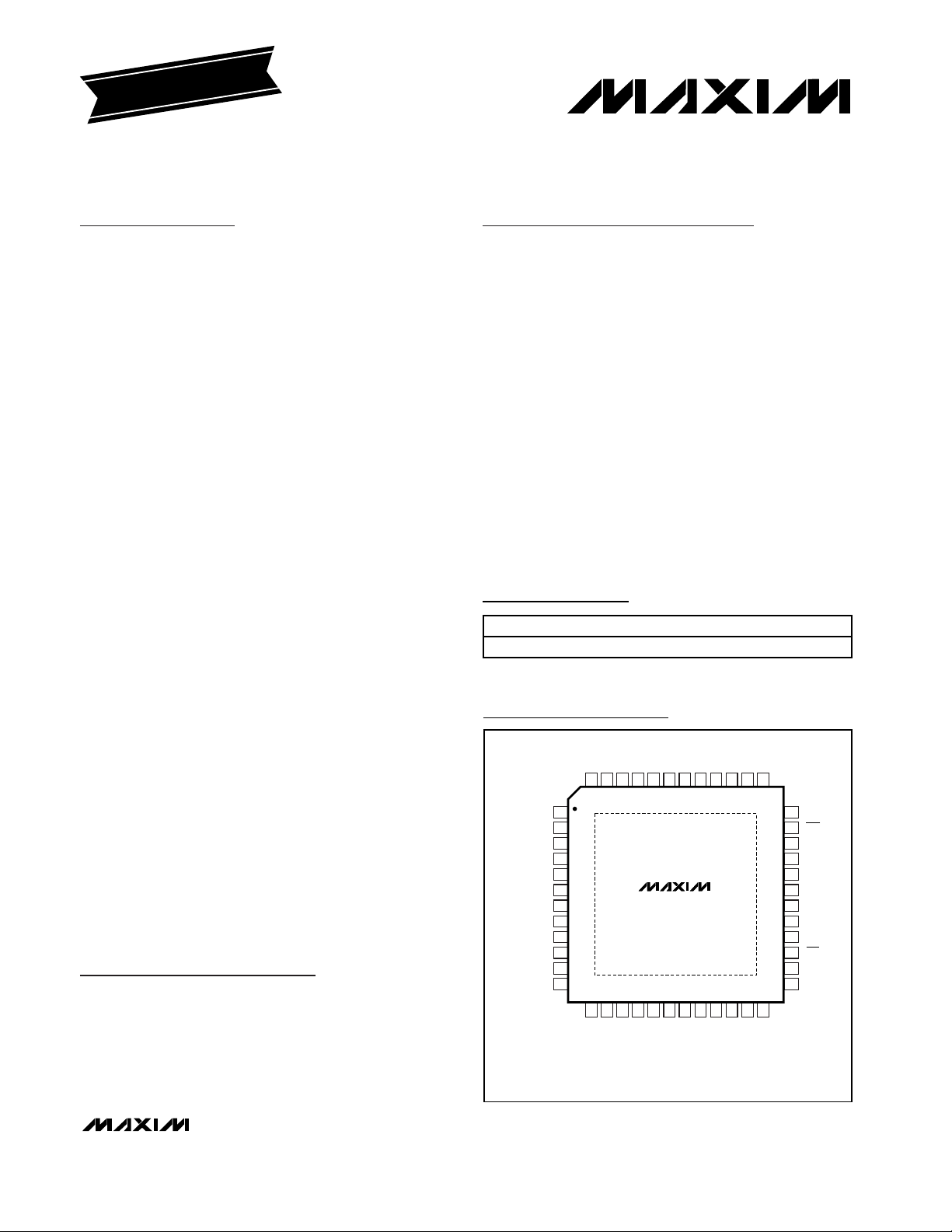
Pin Configuration
*EP = Exposed paddle.
PART TEMP RANGE PIN-PACKAGE
MAX5858AECM -40°C to +85°C 48 TQFP-EP*
DD
DD
AV
DV
DGND
OUTPA
48 47 46 45 44 43EP42 41 40 39 38 37
1
DA9/PD
DA8/DACEN
DA7/F2EN
DA6/F1EN
2
3
4
5
DA5/G3
6
DGND
DV
7
DD
8
DA4/G2
9
DA3/G1
10
DA2/G0
DA1
11
12
DA0
13 14 15 16 17 18 19 20 21 22 23 24
DB9
NOTE: EXPOSED PADDLE CONNECTED TO GND.
DB8
MAX5858A
DB7
DB6
TQFP-EP
OUTNA
DB5
DV
AGND
DD
OUTPB
DGND
OUTNB
CLK
AV
IDE
DD
N.C.
REFR
N.C.
REFO
36
35
REN
34
PLLF
33
PGND
PV
32
DD
31
CLKXN
30
CLKXP
PLLEN
29
28
LOCK
27
CW
26
DB0
DB1
25
DB2
DB3
DB4
Page 2
MAX5858A
Dual, 10-Bit, 300Msps, DAC with 4x/2x/1x
Interpolation Filters and PLL
2 _______________________________________________________________________________________
ABSOLUTE MAXIMUM RATINGS
ELECTRICAL CHARACTERISTICS
(AVDD= DVDD= PVDD= 3V, AGND = DGND = PGND = 0, f
DAC
= 165Msps, no interpolation, PLL disabled, external reference,
V
REFO
= 1.2V, IFS= 20mA, output amplitude = 0dB FS, differential output, TA= T
MIN
to T
MAX
, unless otherwise noted. TA> +25°C
guaranteed by production test. T
A
< +25°C guaranteed by design and characterization. Typical values are at TA= +25°C.)
Stresses beyond those listed under “Absolute Maximum Ratings” may cause permanent damage to the device. These are stress ratings only, and functional
operation of the device at these or any other conditions beyond those indicated in the operational sections of the specifications is not implied. Exposure to
absolute maximum rating conditions for extended periods may affect device reliability.
AVDD, DVDD, PVDDto AGND, DGND, PGND ..........-0.3V to +4V
DA9–DA0, DB9–DB0, CW, REN, PLLF, PLLEN to AGND,
DGND, PGND........................................................-0.3V to +4V
IDE to AGND, DGND, PGND ...................-0.3V to (DV
DD
+ 0.3V)
CLKXN, CLKXP to PGND .........................................-0.3V to +4V
OUTP_, OUTN_ to AGND.......................-1.25V to (AV
DD
+ 0.3V)
CLK, LOCK to DGND...............................-0.3V to (DVDD+ 0.3V)
REFR, REFO to AGND .............................-0.3V to (AV
DD
+ 0.3V)
AGND to DGND, DGND to PGND,
AGND to PGND ..................................................-0.3V to +0.3V
Maximum Current into Any Pin
(excluding power supplies) ............................................±50mA
Continuous Power Dissipation (T
A
= +70°C)
48-Pin TQFP-EP (derate 36.2mW/°C above +70°C) ....2.899W
Operating Temperature Range ...........................-40°C to +85°C
Storage Temperature Range .............................-65°C to +150°C
Junction Temperature......................................................+150°C
Lead Temperature (soldering, 10s) .................................+300°C
STATIC PERFORMANCE
Resolution 10 Bits
Integral Nonlinearity INL RL = 0 -1.25 ±0.5 +1.25 LSB
Differential Nonlinearity DNL Guaranteed monotonic, RL = 0 -0.75 ±0.25 +0.75 LSB
Offset Error V
Gain Error (See Gain Error
Parameter Definitions Section)
DYNAMIC PERFORMANCE
Maximum DAC Update Rate f
Glitch Impulse 5 pV-s
Spurious-Free Dynamic Range to
Input Update Rate Nyquist
Spurious-Free Dynamic Range
Within a Window
Multitone Power Ratio, 8 Tones,
~300kHz Spacing
Adjacent Channel Leakage Ratio
with UMTS
PARAMETER SYMBOL CONDITIONS MIN TYP MAX UNITS
OS
GE
DAC
SFDR
SFDR
MTPR f
ACLR f
Internal reference (Note 1) -10 ±1.6 +11
External reference -8 ±1.2 +8
4x/2x interpolation modes 300 Msps
f
= 165Msps
DAC
f
= 300Msps,
DAC
2x interpolation
f
= 200Msps, 2x interpolation,
DAC
f
= 40MHz, span = 20MHz
OUT
f
= 165Msps, f
DAC
span = 4MHz
= 165Msps, f
DAC
=122.88Msps, f
DAC
f
= 5MHz,
OUT
≥ +25°C
T
A
f
= 20MHz 73
OUT
f
= 50MHz 66
OUT
= 70MHz 65
f
OUT
f
= 5MHz 76
OUT
f
= 40MHz 73
OUT
f
= 60MHz 72
OUT
= 5MHz,
OUT
= 20MHz 76 dBc
OUT
= 30.72MHz 63 dB
OUT
-0.5 ±0.1 +0.5 LSB
68 76
85
76.5 85
%
dBc
dBc
Page 3
MAX5858A
Dual, 10-Bit, 300Msps, DAC with 4x/2x/1x
Interpolation Filters and PLL
_______________________________________________________________________________________ 3
ELECTRICAL CHARACTERISTICS (continued)
(AVDD= DVDD= PVDD= 3V, AGND = DGND = PGND = 0, f
DAC
= 165Msps, no interpolation, PLL disabled, external reference,
V
REFO
= 1.2V, IFS= 20mA, output amplitude = 0dB FS, differential output, TA= T
MIN
to T
MAX
, unless otherwise noted. TA> +25°C
guaranteed by production test. T
A
< +25°C guaranteed by design and characterization. Typical values are at TA= +25°C.)
Total Harmonic Distortion to
Nyquist
Noise Spectral Density n
Output Channel-to-Channel
Isolation
Gain Mismatch Between
Channels
Phase Mismatch Between
Channels
Wideband Output Noise 50 pA/√Hz
ANALOG OUTPUT
Full-Scale Output Current Range I
Output Voltage Compliance
Range
Output Leakage Current Power-down or standby mode -5 +5 µA
REFERENCE
Reference Output Voltage V
Output-Voltage Temperature Drift TCV
Reference Output Drive
Capability
Reference Input Voltage Range REN = AV
Reference Supply Rejection 0.2 mV/V
Current Gain IFS/I
INTERPOLATION FILTER (2x interpolation)
Passband Width
Stopband Rejection
Group Delay 18
PARAMETER SYMBOL CONDITIONS MIN TYP MAX UNITS
THD f
D
FS
REF0
REF
REF
f
/
OUT
0.5f
DAC
= 165Msps, f
DAC
f
= 165Msps, f
DAC
= 5MHz 80 dB
f
OUT
f
= 5MHz ±0.05 dB
OUT
f
= 5MHz ±0.15 Degrees
OUT
REN = AGND 1.14 1.24 1.34 V
DD
-0.005dB 0.398
-0.01dB 0.402
-0.1dB 0.419
-3dB 0.478
0.604f
0.600f
0.594f
0.532f
/ 2 to 1.396f
DAC
/ 2 to 1.400f
DAC
/ 2 to 1.406f
DAC
/ 2 to 1.468f
DAC
= 5MHz -72 dBc
OUT
= 5MHz -143 dBm/Hz
OUT
/ 2 74
DAC
/ 2 62
DAC
/ 2 53
DAC
/ 2 14
DAC
220mA
-1.0 +1.25 V
±50 ppm/°C
50 µA
0.10 1.32 V
32 mA/mA
MHz/
MHz
dB
Data
clock
cycles
Impulse Response Duration 22
Data
clock
cycles
Page 4
MAX5858A
Dual, 10-Bit, 300Msps, DAC with 4x/2x/1x
Interpolation Filters and PLL
4 _______________________________________________________________________________________
ELECTRICAL CHARACTERISTICS (continued)
(AVDD= DVDD= PVDD= 3V, AGND = DGND = PGND = 0, f
DAC
= 165Msps, no interpolation, PLL disabled, external reference,
V
REFO
= 1.2V, IFS= 20mA, output amplitude = 0dB FS, differential output, TA= T
MIN
to T
MAX
, unless otherwise noted. TA> +25°C
guaranteed by production test. T
A
< +25°C guaranteed by design and characterization. Typical values are at TA= +25°C.)
INTERPOLATION FILTER (4x interpolation)
Passband Width
PARAMETER SYMBOL CONDITIONS MIN TYP MAX UNITS
Stopband Rejection
Group Delay 22
Impulse Response Duration 27
LOGIC INPUTS (IDE, CW, REN, DA9–DA0, DB9–DB0, PLLEN)
Digital Input-Voltage High V
Digital Input-Voltage Low V
Digital Input-Current High I
Digital Input-Current Low I
Digital Input Capacitance C
DIGITAL OUTPUTS (CLK, LOCK)
Digital Output-Voltage High V
Digital Output-Voltage Low V
DIFFERENTIAL CLOCK INPUT (CLKXP, CLKXN)
Clock Input Internal Bias PV
Differential Clock Input Swing 0.5 V
Clock Input Impedance Single-ended clock drive 5 kΩ
TIMING CHARACTERISTICS
Input Data Rate f
Clock Frequency at CLK Input f
-0.005dB 0.200
f
0.5f
OUT
OH
DATA
CLK
-0.01dB 0.201
/
DAC
-0.1dB 0.210
-3dB 0.239
0.302f
0.300f
0.297f
0.266f
IH
IL
VIH = 2V -1 +1 µA
H
VIL = 0.8V -1 +1 µA
IL
IN
I
SOURCE
I
OL
SINK
No interpolation 165
2x interpolation
4x interpolation
No interpolation, PLL enabled 165
2x interpolation, PLL enabled 75 150
4x interpolation, PLL enabled 37.5 75
/ 2 to 1.698f
DAC
/ 2 to 1.700f
DAC
/ 2 to 1.703 f
DAC
/ 2 to 1.734f
DAC
= 0.5mA, Figure 1
= 0.5mA, Figure 1
/ 2 74
DAC
/ 2 63
DAC
/ 2 53
DAC
/ 2 14
DAC
PLL disabled 150
PLL enabled 75 150
PLL disabled 75
PLL enabled 37.5 75
2V
3pF
0.9 ×
DV
DD
/ 2 V
DD
0.8 V
0.1 ×
DV
DD
MHz/
MHz
dB
Data
clock
cycles
Data
clock
cycles
V
V
P-P
Msps
MHz
Page 5
MAX5858A
Dual, 10-Bit, 300Msps, DAC with 4x/2x/1x
Interpolation Filters and PLL
_______________________________________________________________________________________ 5
ELECTRICAL CHARACTERISTICS (continued)
(AVDD= DVDD= PVDD= 3V, AGND = DGND = PGND = 0, f
DAC
= 165Msps, no interpolation, PLL disabled, external reference,
V
REFO
= 1.2V, IFS= 20mA, output amplitude = 0dB FS, differential output, TA= T
MIN
to T
MAX
, unless otherwise noted. TA> +25°C
guaranteed by production test. T
A
< +25°C guaranteed by design and characterization. Typical values are at TA= +25°C.)
Output Settling Time t
Output Rise Time 10% to 90% (Note 2) 2.5 ns
Output Fall Time 90% to 10% (Note 2) 2.5 ns
Data-to-CLK Rise Setup Time
(Note 3)
Data-to-CLK Rise Hold Time
(Note 3)
Data-to-CLK Fall Setup Time
(Note 3)
Data-to-CLK Fall Hold Time
(Note 3)
Control Word to CW Fall Setup
Time
Control Word to CW Fall Hold
Time
CW High Time 5ns
CW Low Time 5ns
DACEN Rise-to-V
PD Fall-to-V
Clock Frequency at
CLKXP/CLKXN Input
CLKXP/CLKXN Differential Clock
Input to CLK Output Delay
Minimum CLKXP/CLKXN Clock
High Time
Minimum CLKXP/CLKXN Clock
Low Time
POWER REQUIREMENTS
Analog Power-Supply Voltage AV
Analog Supply Current I
Digital Power-Supply Voltage DV
PARAMETER SYMBOL CONDITIONS MIN TYP MAX UNITS
Stable t
OUT
Stable t
OUT
To ±0.1% error band (Note 2) 11 ns
s
t
DCSR
t
DCHR
t
DCSF
t
DCHF
t
CWS
t
CWH
STB
PDSTB
f
CLKDIFF
t
CXD
t
CXH
t
CXL
AVDD
PLL disabled 1.5
PLL enabled 2.2
PLL disabled 0.4
PLL enabled 1.4
PLL disabled 1.8
PLL enabled 2.4
PLL disabled 1.2
PLL enabled 1.3
External reference 0.5 ms
Differential clock, PLL disabled 300 MHz
PLL disabled 4.6 ns
DD
(Note 4) 45 49 mA
DD
2.5 ns
2.5 ns
0.7 µs
1.5 ns
1.5 ns
2.7 3.3 V
2.7 3.3 V
ns
ns
ns
ns
Page 6
MAX5858A
Dual, 10-Bit, 300Msps, DAC with 4x/2x/1x
Interpolation Filters and PLL
6 _______________________________________________________________________________________
ELECTRICAL CHARACTERISTICS (continued)
(AVDD= DVDD= PVDD= 3V, AGND = DGND = PGND = 0, f
DAC
= 165Msps, no interpolation, PLL disabled, external reference,
V
REFO
= 1.2V, IFS= 20mA, output amplitude = 0dB FS, differential output, TA= T
MIN
to T
MAX
, unless otherwise noted. TA> +25°C
guaranteed by production test. T
A
< +25°C guaranteed by design and characterization. Typical values are at TA= +25°C.)
Note 1: Including the internal reference voltage tolerance.
Note 2: Measured single ended with 50Ω load and complementary output connected to ground.
Note 3: Guaranteed by design, not production tested.
Note 4: Tested with an output frequency of f
OUT
= 5MHz.
Note 5: All digital inputs at 0 or DV
DD
. Clock signal disabled.
Figure 1. Load Test Circuit for CLK Outputs
Digital Supply Current (Note 4) I
PARAMETER SYMBOL CONDITIONS MIN TYP MAX UNITS
PLL Power-Supply Voltage PV
PLL Supply Current (Note 4) I
Standby Current I
Power-Down Current I
Total Power Dissipation
(Note 4)
f
DAC
DVDD
PVDD
STANDBY
PD
P
TOT
DAC
f
DAC
DD
f
DAC
f
DAC
f
DAC
interpolation
(Note 5) 4.4 4.8 mA
(Note 5) 1 µA
f
DAC
DAC
f
DAC
= 60Msps
= 165Msps
= 200Msps
= 60Msps 17
= 165Msps 46 52
= 200Msps, 2x interpolation or 4x
= 60Msps
= 165Msps
= 200Msps
No interpolation 34
2x interpolation 75
4x interpolation 72
No interpolation 54 61
2x interpolation 146f
4x interpolation 140
2x interpolation 172 186
4x interpolation 165 178
No interpolation 324
2x interpolation 487
4x interpolation 498
No interpolation 438 486
2x interpolation 735f
4x interpolation 721
2x interpolation 816
4x interpolation 795
2.7 3.3 V
mA
mA
55 61
mW
TO OUTPUT
PIN
5pF
0.5mA
0.5mA
1.6V
Page 7
MAX5858A
Dual, 10-Bit, 300Msps, DAC with 4x/2x/1x
Interpolation Filters and PLL
_______________________________________________________________________________________ 7
)
Typical Operating Characteristics
(AVDD= DVDD= PVDD= 3V, AGND = DGND = PGND = 0, external reference = 1.2V, no interpolation, PLL disabled, IFS= 20mA,
differential output, T
A
= +25°C, unless otherwise noted.)
SPURIOUS-FREE DYNAMIC RANGE
vs. OUTPUT FREQUENCY
(NO INTERPOLATION, f
100
90
80
70
60
50
SFDR (dBc)
40
30
20
10
A
A
OUT
PLL DISABLED
0
0 102030405060708090
SPURIOUS-FREE DYNAMIC RANGE
(2x INTERPOLATION, f
100
A
90
80
70
60
50
SFDR (dBc)
40
30
20
10
OUT
A
OUT
PLL ENABLED
0
080
SPURIOUS-FREE DYNAMIC RANGE
vs. OUTPUT FREQUENCY
DAC
= -6dBFS
OUT
= -12dBS
OUTPUT FREQUENCY (MHz)
A
= 165MHz)
= 0dBFS
OUT
MAX5858A toc01
(NO INTERPOLATION, f
100
A
= -6dBFS
90
80
70
60
A
OUT
50
SFDR (dBc)
40
30
20
10
PLL DISABLED
0
035
OUT
= -12dBFS
OUTPUT FREQUENCY (MHz)
SPURIOUS-FREE DYNAMIC RANGE
vs. OUTPUT FREQUENCY
= 300MHz)
DAC
= -6dBFS
= -12dBFS
OUTPUT FREQUENCY (MHz)
40302010 706050
A
OUT
= 0dBFS
MAX5858A toc04
100
90
80
70
60
50
SFDR (dBc)
40
30
20
10
0
vs. OUTPUT FREQUENCY
(2x INTERPOLATION, f
A
= -6dBFS
OUT
A
= 0dBFS
OUT
PLL DISABLED
045
2015105403530
OUTPUT FREQUENCY (MHz)
SPURIOUS-FREE DYNAMIC RANGE
vs. OUTPUT FREQUENCY
(4x INTERPOLATION, f
100
A
= -6dBFS
OUT
90
80
70
60
A
= 0dBFS
50
SFDR (dBc)
40
30
20
10
0
OUT
PLL ENABLED
040
OUTPUT FREQUENCY (MHz)
DAC
2015105353025
= 300MHz)
A
= -12dBFS
OUT
MAX5858A toc07
DAC
20151053025
DAC
A
OUT
25
= 65MHz)
A
= 0dBFS
OUT
= 165MHz)
= -12dBFS
SPURIOUS-FREE DYNAMIC RANGE
vs. OUTPUT FREQUENCY
DAC
40302010 706050
= 300MHz)
A
= -12dBFS
OUT
MAX5858A toc02
(2x INTERPOLATION, f
100
A
= -6dBFS
90
80
70
60
50
SFDR (dBc)
40
30
20
10
0
OUT
A
= 0dBFS
OUT
PLL DISABLED
080
OUTPUT FREQUENCY (MHz)
SPURIOUS-FREE DYNAMIC RANGE
vs. OUTPUT FREQUENCY
= 165MHz)
DAC
A
OUT
= 0dBFS
MAX5858A toc05
(4x INTERPOLATION, f
100
SFDR (dBc)
A
= -6dBFS
90
80
70
60
50
40
30
20
10
OUT
A
= -12dBFS
OUT
PLL DISABLED
0
03691215 18 21
OUTPUT FREQUENCY (MHz)
SPURIOUS-FREE DYNAMIC RANGE
vs. OUTPUT FREQUENCY
(4x INTERPOLATION, f
100
SFDR (dBc)
A
= -6dBFS
90
80
70
60
50
40
30
20
10
OUT
A
= 0dBFS
OUT
PLL DISABLED
0
040
OUTPUT FREQUENCY (MHz
DAC
A
2015105353025
= 300MHz)
= -12dBFS
OUT
MAX5858A toc08
MAX5858A toc03
MAX5858A toc06
Page 8
MAX5858A
Dual, 10-Bit, 300Msps, DAC with 4x/2x/1x
Interpolation Filters and PLL
8 _______________________________________________________________________________________
Typical Operating Characteristics (continued)
(AVDD= DVDD= PVDD= 3V, AGND = DGND = PGND = 0, external reference = 1.2V, no interpolation, PLL disabled, IFS= 20mA,
differential output, T
A
= +25°C, unless otherwise noted.)
SPURIOUS-FREE DYNAMIC RANGE
vs. OUTPUT FREQUENCY
(NO INTERPOLATION, f
DAC
= 165MHz)
MAX5858A toc10
OUTPUT FREQUENCY (MHz)
SFDR (dBc)
807050 6020 30 4010
10
20
30
40
50
60
70
80
90
100
0
090
TA = -10°C
TA = +25°C
TA = +85°C
-100
-60
-70
-80
-90
-40
-50
-20
-30
-10
0
7.8 11.4
FFT PLOT
(±2MHz WINDOW)
MAX5858A toc11
OUTPUT FREQUENCY (MHz)
OUTPUT POWER (dBm)
9.49.08.68.2 11.010.610.29.8
f
DAC
= 165MHz
f
OUT
= 10MHz
A
OUT
= -6dBFS
-100
-60
-70
-80
-90
-40
-50
-20
-30
-10
0
0
8.25
16.50
24.75
33.00
41.25
49.50
57.75
66.00
74.25
82.50
FFT PLOT FOR DAC UPDATE NYQUIST WINDOW
(NO INTERPOLATION, f
DAC
= 165MHz,
f
OUT
= 10MHz, A
OUT
= 0dBFS)
MAX5858A toc12
OUTPUT FREQUENCY (MHz)
OUTPUT POWER (dBm)
0 102030405060708090100
FFT PLOT FOR DAC UPDATE NYQUIST
WINDOW (2x INTERPOLATION,
f
DAC
= 200MHz, f
OUT
= 10MHz, A
OUT
= 0dBFS)
MAX5858A toc13
OUTPUT FREQUENCY (MHz)
OUTPUT POWER (dBm)
-100
-60
-70
-80
-90
-40
-50
-20
-30
-10
0
0 102030405060708090100
FFT PLOT FOR DAC UPDATE NYQUIST
WINDOW (4x INTERPOLATION,
f
DAC
= 200MHz, f
OUT
= 10MHz, A
OUT
= 0dBFS)
MAX5858A toc14
OUTPUT FREQUENCY (MHz)
OUTPUT POWER (dBm)
-100
-60
-70
-80
-90
-40
-50
-20
-30
-10
0
SPURIOUS-FREE DYNAMIC RANGE
vs. TEMPERATURE (NO INTERPOLATION,
f
DAC
= 165MHz, f
OUT
= 5MHz)
MAX5858A toc09
TEMPERATURE (°C)
SFDR (dBc)
603510-15
10
20
30
40
50
60
70
80
90
100
0
-40 85
A
OUT
= -12dBFS
A
OUT
= -6dBFS
A
OUT
= 0dBFS
Page 9

MAX5858A
Dual, 10-Bit, 300Msps, DAC with 4x/2x/1x
Interpolation Filters and PLL
_______________________________________________________________________________________ 9
Typical Operating Characteristics (continued)
(AVDD= DVDD= PVDD= 3V, AGND = DGND = PGND = 0, external reference = 1.2V, no interpolation, PLL disabled, IFS= 20mA,
differential output, T
A
= +25°C, unless otherwise noted.)
-100
-30
-40
-10
-20
-70
-80
-90
-50
-60
0
4.5 4.7 4.9 5.1 5.3 5.5
2-TONE IMD PLOT
(NO INTERPOLATION, f
DAC
= 165MHz)
MAX5858A toc15
OUTPUT FREQUENCY (MHz)
OUTPUT POWER (dBm)
A
OUT
= -6dBFS
BW = 1MHz
fT1 = 4.9448MHz
f
T2
= 5.0656MHz
2 x fT1 - f
T2
f
T1
f
T2
2 x fT2 - f
T1
-100
-30
-40
-10
-20
-70
-80
-90
-50
-60
0
18.5 19.0 19.5 20.0 20.5 21.0 21.5
8-TONE MTPR PLOT (NO INTERPOLATION,
f
DAC
= 165MHz, f
CENTER
= 19.9503MHz)
OUTPUT FREQUENCY (MHz)
OUTPUT POWER (dBm)
MAX5858A toc16
A
OUT
= -18dB FS
BW = 3MHz
fT1 = 18.8022MHz fT5 = 20.2524MHz
f
T2
= 19.0237MHz fT6 = 20.5344MHz
f
T3
= 19.2654MHz fT7 = 20.8365MHz
f
T4
= 19.6481MHz fT8 = 21.1386MHz
f
T4
f
T5
f
T1
f
T2
f
T3
f
T6
f
T7
f
T8
-100
-30
-40
-10
-20
-70
-80
-90
-50
-60
0
28.5 29.0 29.5 30.0 30.5 31.0 31.5
8-TONE MTPR PLOT (4x INTERPOLATION,
f
DAC
= 286.4MHz, f
CENTER
= 29.9572MHz)
MAX5858A toc17
OUTPUT FREQUENCY (MHz)
OUTPUT POWER (dBm)
A
OUT
= -18dBFS
BW = 3MHz
fT1 = 28.7597MHz fT5 = 30.2281MHz
f
T2
= 29.1008MHz fT6 = 30.5952MHz
f
T3
= 29.3628MHz fT7 = 30.8924MHz
f
T4
= 29.6862MHz fT8 = 31.1546MHz
f
T4
f
T5
f
T1
f
T2
f
T3
f
T6
f
T7
f
T8
-100
-30
-40
-20
-10
-70
-80
-90
-60
-50
-1
1.00
9.15
17.30
25.25
33.60
41.75
49.90
58.05
66.20
74.35
82.50
8-TONE MTPR PLOT FOR NYQUIST WINDOW
(NO INTERPOLATION, f
DAC
= 165MHz,
f
CENTER
= 19.9569MHz, A
OUT
= -18dBFS)
MAX5858A toc18
OUTPUT FREQUENCY (MHz)
OUTPUT POWER (dBm)
MTPR = 76dBc
-100
-40
-50
-30
-20
-80
-90
-70
-60
0
-10
1.0
15.2
28.6
42.9
57.2
71.5
85.8
100.1
114.4
128.7
143.2
8-TONE MTPR PLOT FOR NYQUIST WINDOW
(4x INTERPOLATION, f
DAC
= 286.4MHz, f
CENTER
= 20MHz,
INPUT TONES SPACING ~ 300kHz, A
OUT
= -18dBFS)
MAX5858A toc19
OUTPUT FREQUENCY (MHz)
OUTPUT POWER (dBm)
A
B
35.8MHz
A: IN-BAND-RANGE
B: OUT-OF-BAND RANGE
-30
-40
-50
-60
-70
-80
-90
-100
-10
-20
0 61.44
ACLR UMTS PLOT
(NO INTERPOLATION, f
DAC
= 122.88MHz,
f
DATA
= 122.88MHz, f
CENTER
= 30.72MHz)
MAX5858A toc20
6.14MHz/div
OUTPUT POWER (dBm)
OUTPUT FREQUENCY (MHz)
ACLR = 63dB
Page 10
MAX5858A
Dual, 10-Bit, 300Msps, DAC with 4x/2x/1x
Interpolation Filters and PLL
10 ______________________________________________________________________________________
Typical Operating Characteristics (continued)
(AVDD= DVDD= PVDD= 3V, AGND = DGND = PGND = 0, external reference = 1.2V, no interpolation, PLL disabled, IFS= 20mA,
differential output, T
A
= +25°C, unless otherwise noted.)
-30
-40
-50
-60
-70
-80
-90
-100
-0
-10
-20
0 122.88
ACLR WITH UMTS PLOT
(NO INTERPOLATION, f
DAC
= 122.88MHz,
f
DATA
= 122.88MHz, f
CENTER
= 30.72MHz)
MAX5858A toc21
OUTPUT FREQUENCY (MHz)
OUTPUT POWER (dBm)
12.288MHz/div
ACLR = 63dB
0 61.44
ACLR WITH UMTS PLOT
(2x INTERPOLATION, f
DAC
= 245.76MHz,
f
DATA
= 122.88MHz, f
CENTER
= 30.72MHz)
MAX5858A toc22
OUTPUT FREQUENCY (MHz)
OUTPUT POWER (dBm)
6.14MHz/div
-30
-40
-50
-60
-70
-80
-90
-100
-0
-10
-20
ACLR = 63dB
0 122.88
ACLR WITH UMTS PLOT
(2x INTERPOLATION, f
DAC
= 245.76MHz,
f
DATA
= 122.88MHz, f
CENTER
= 30.72MHz)
MAX5858A toc23
OUTPUT FREQUENCY (MHz)
OUTPUT POWER (dBm)
12.288MHz/div
-30
-40
-50
-60
-70
-80
-90
-100
-0
-10
-20
ACLR = 63dB
FFT PLOT FOR PLL DISABLED
AND PLL ENABLED
(f
OUT
= 10MHz, 2x INTERPOLATION)
MAX5858A toc24
OUTPUT FREQUENCY (MHz)
OUTPUT POWER (dBm)
1MHz/div515
-30
-20
-10
-40
-50
-60
-70
-80
-90
-100
-110
-120
0
PLL ENABLED
PLL DISABLED
PHASE NOISE WITH PLL DISABLED
AND ENABLED
(f
OUT
= f
DATA
/4, 2x INTERPOLATION)
MAX5858A toc25
OFFSET FREQUENCY (MHz)
NOISE DENSITY (dBm/Hz)
0.5MHz/div
0
5
-40
-50
-60
-70
-80
-90
-100
-110
-120
-130
-140
-150
-30
PLL ENABLED f
DATA
= 125MHz
PLL ENABLED f
DATA
= 100MHz
PLL ENABLED f
DATA
= 150MHz
PLL DISABLED f
DATA
= 75MHz
-0.5
-0.2
-0.3
-0.4
0
-0.1
0.4
0.3
0.2
0.1
0.5
0 150 300 450 600 750 900 1050
INTEGRAL NONLINEARITY
vs. DIGITAL INPUT CODE
MAX5858A toc26
DIGITAL INPUT CODE
INL (LSB)
RL = 0
Page 11

MAX5858A
Dual, 10-Bit, 300Msps, DAC with 4x/2x/1x
Interpolation Filters and PLL
______________________________________________________________________________________ 11
Typical Operating Characteristics (continued)
(AVDD= DVDD= PVDD= 3V, AGND = DGND = PGND = 0, external reference = 1.2V, no interpolation, PLL disabled, IFS= 20mA,
differential output, TA= +25°C, unless otherwise noted.)
-0.30
-0.10
-0.20
0
0.20
0.10
0.30
0 150 300 450 600 750 900 1050
DIFFERENTIAL NONLINEARITY
vs. DIGITAL INPUT CODE
MAX5858A toc27
DIGITAL INPUT CODE
INL (LSB)
RL = 0
200
300
250
400
350
450
0 165
POWER DISSIPATION
vs. f
DAC
MAX5858A toc28
f
DAC
(MHz)
POWER DISSIPATION (mW)
6834 102 136
f
OUT
= 5MHz
NO INTERPOLATION
350
550
450
950
750
850
650
1050
0 300
POWER DISSIPATION
vs. f
DAC
MAX5858A toc28
f
DAC
(MHz)
POWER DISSIPATION (mW)
15010050 200 250
4x INTERPOLATION
2x INTERPOLATION
POWER DISSIPATION
vs. SUPPLY VOLTAGE
MAX5858A toc30
SUPPLY VOLTAGE (V)
POWER DISSIPATION (mW)
3.23.12.8 2.9 3.0
300
400
500
600
700
800
900
1000
200
2.7 3.3
2x INTERPOLATION
f
CLK
= 200MHz
f
OUT
= 5MHz
NO INTERPOLATION
f
CLK
= 165MHz
f
OUT
= 5MHz
4x INTERPOLATION
f
CLK
= 200MHz
f
OUT
= 5MHz
1.20
1.22
1.21
1.24
1.23
1.26
1.25
1.27
1.28
2.7 3.33.2
INTERNAL REFERENCE VOLTAGE
vs. SUPPLY VOLTAGE
MAX5858A toc31
SUPPLY VOLTAGE (V)
INTERNAL REFERENCE VOLTAGE (V)
2.92.8 3.0 3.1
1.20
1.22
1.21
1.24
1.23
1.26
1.25
1.27
1.28
-40 85
INTERNAL REFERENCE VOLTAGE
vs. TEMPERATURE
MAX5858A toc32
TEMPERATURE (°C)
INTERNAL REFERENCE VOLTAGE (V)
10-15 35 60
Page 12

MAX5858A
Dual, 10-Bit, 300Msps, DAC with 4x/2x/1x
Interpolation Filters and PLL
12 ______________________________________________________________________________________
Pin Description
Typical Operating Characteristics (continued)
(AVDD= DVDD= PVDD= 3V, AGND = DGND = PGND = 0, external reference = 1.2V, no interpolation, PLL disabled, IFS= 20mA,
differential output, T
A
= +25°C, unless otherwise noted.)
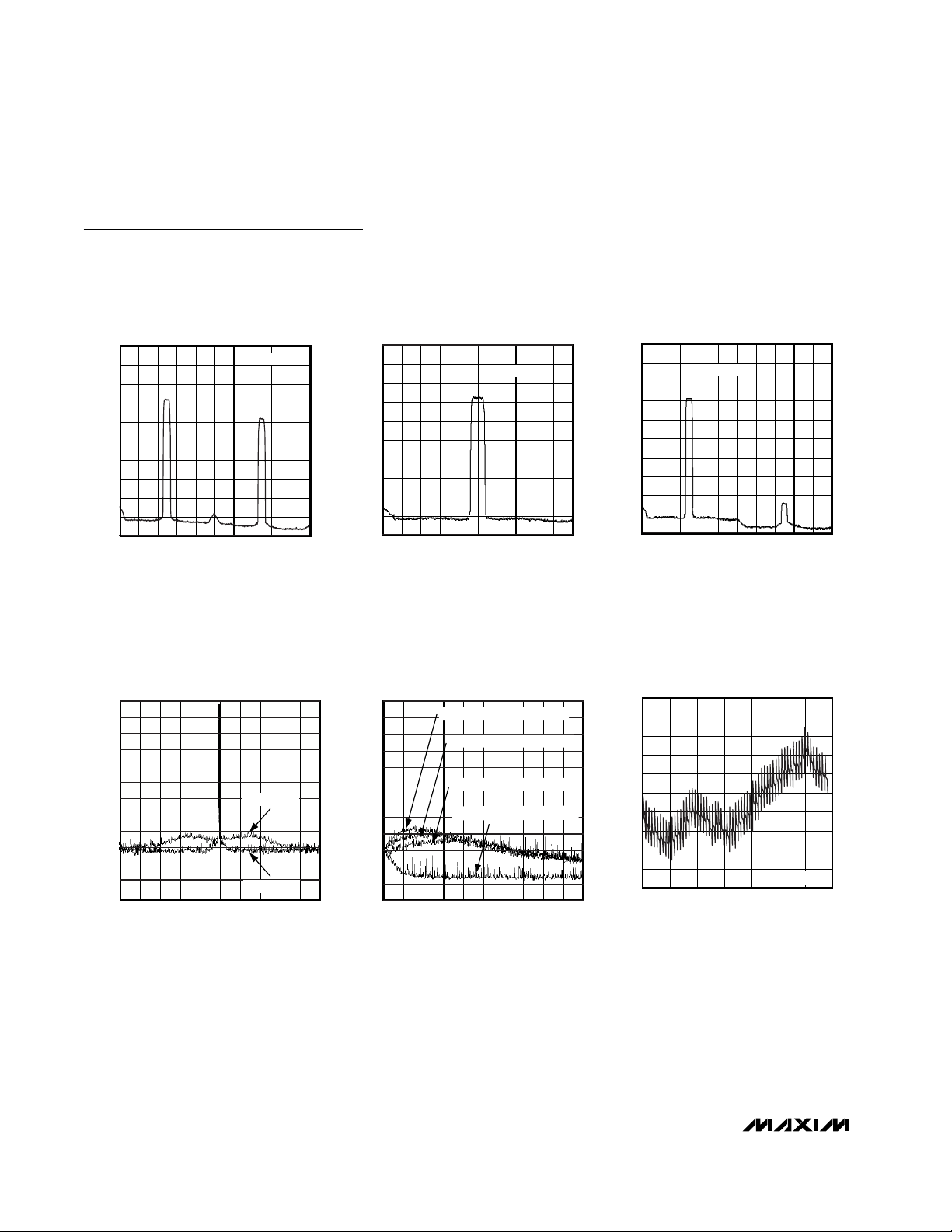
DYNAMIC RESPONSE RISE TIME
10ns/div
PIN NAME FUNCTION
1 DA9/PD
2 DA8/DACEN
3 DA7/F2EN
4 DA6/F1EN
5 DA5/G3 Channel A Input Data Bit 5/Channel A Gain Adjustment Bit 3
6, 19, 47 DGND Digital Ground
7, 18, 48 DV
8 DA4/G2 Channel A Input Data Bit 4/Channel A Gain Adjustment Bit 2
9 DA3/G1 Channel A Input Data Bit 3/Channel A Gain Adjustment Bit 1
10 DA2/G0 Channel A Input Data Bit 2/Channel A Gain Adjustment Bit 0
11 DA1 Channel A Input Data Bit 1
12 DA0 Channel A Input Data Bit 0 (LSB)
DD
MAX5858A toc33
RL = 50Ω
SINGLE ENDED
200mV/div
DYNAMIC RESPONSE FALL TIME
RL = 50Ω
SINGLE ENDED
10ns/div
MAX5858A toc34
Channel A Input Data Bit 9 (MSB)/Power-Down Control Bit:
0: Enter DAC standby mode (DACEN = 0) or power up DAC (DACEN = 1).
1: Enter power-down mode.
Channel A Input Data Bit 8/DAC Enable Control Bit:
0: Enter DAC standby mode with PD = 0.
1: Power up DAC with PD = 0.
X: Enter power-down mode with PD = 1 (X = don’t care.)
Channel A Input Data Bit 7/Second Interpolation Filter Enable Bit:
0: Interpolation mode is determined by F1EN.
1: Enable 4x interpolation mode. (F1EN must equal 1.)
Channel A Input Data Bit 6/First Interpolation Filter Enable Bit:
0: Interpolation disable.
1: Enable 2x interpolation.
Digital Power Supply. See Power Supplies, Bypassing, Decoupling, and Layout section.
200mV/div
Page 13

MAX5858A
Dual, 10-Bit, 300Msps, DAC with 4x/2x/1x
Interpolation Filters and PLL
______________________________________________________________________________________ 13
Pin Description (continued)
PIN NAME FUNCTION
13 DB9 Channel B Input Data Bit 9 (MSB)
14 DB8 Channel B Input Data Bit 8
15 DB7 Channel B Input Data Bit 7
16 DB6 Channel B Input Data Bit 6
17 DB5 Channel B Input Data Bit 5
20 CLK
21 IDE
22 DB4 Channel B Input Data Bit 4
23 DB3 Channel B Input Data Bit 3
24 DB2 Channel B Input Data Bit 2
25 DB1 Channel B Input Data Bit 1
26 DB0 Channel B Input Data Bit 0 (LSB)
27 CW Active-Low Control-Word Write Pulse. The control word is latched on the falling edge of CW.
28 LOCK PLL Lock Signal Output. High level indicates that PLL is locked to the CLK signal.
29 PLLEN PLL Enabled Input. PLL in enabled when PLLEN is high.
30 CLKXP
31 CLKXN
32 PV
33 PGND PLL Ground
34 PLLF
35 REN Active-Low Reference Enable. Connect REN to AGND to activate the on-chip 1.24V reference.
36 REFO
37, 38 N.C. No Connection. Not connected internally.
39 REFR
40, 46 AV
41 OUTNB Channel B Negative Analog Current Output
42 OUTPB Channel B Positive Analog Current Output
43 AGND Analog Ground
44 OUTNA Channel A Negative Analog Current Output
45 OUTPA Channel A Positive Analog Current Output
— EP Exposed Paddle. Connect to the ground plane.
DD
DD
Clock Output/Input. CLK becomes an input when the PLL is enabled. CLK is an output when the PLL
is disabled.
Interleave Data Mode Enable. When IDE is high, data for both DAC channels is written through port A
(bits DA9–DA0). When IDE is low, channel A data is latched on the rising edge of CLK and channel B
data is latched on the falling edge of CLK.
Differential Clock Input Positive Terminal. Connect to PGND when the PLL is enabled. Bypass CLKXP
with a 0.01µF capacitor to PGND when CLKXN is in single-ended mode.
Differential Clock Input Negative Terminal. Connect to PV
with a 0.01µF capacitor to PGND when CLKXP is in single-ended mode.
PLL Power Supply. See Power Supplies, Bypassing, Decoupling, and Layout section.
PLL Loop Filter. Connect a 4.12kΩ resistor in series with a 100pF capacitor between PLLF and
PGND.
Reference I/O. REFO serves as the reference input when the internal reference is disabled. If the
internal 1.24V reference is enabled, REFO serves as the output for the internal reference. When the
internal reference is enabled, bypass REFO to AGND with a 0.1µF capacitor.
Full-Scale Current Adjustment. To set the output full-scale current, connect an external resistor R
between REFR and AGND. The output full-scale current is equal to 32 × V
Analog Power Supply. See Power Supplies, Bypassing, Decoupling, and Layout section.
when the PLL is enabled. Bypass CLKXN
DD
REFO/RSET
.
SET
Page 14

MAX5858A
Dual, 10-Bit, 300Msps, DAC with 4x/2x/1x
Interpolation Filters and PLL
14 ______________________________________________________________________________________
Detailed Description
The MAX5858A dual, high-speed, 10-bit, current-output
DAC provides superior performance in communication
systems requiring low-distortion analog-signal reconstruction. The MAX5858A combines two DAC cores with
2x/4x programmable digital interpolation filters, a PLL
clock multiplier, divide-by-N clock output, and an onchip 1.24V reference. The current outputs of the DACs
can be configured for differential or single-ended operation. The full-scale output current range is adjustable
from 2mA to 20mA to optimize power dissipation and
gain control.
The MAX5858A accepts an input data rate of up to
165MHz or a DAC conversion rate of up to 300MHz. The
inputs are latched on the rising edge of the clock whereas the output latches on the following rising edge.
The two-stage digital interpolation filters are programmable to 4x, 2x, or no interpolation. When operating in
4x interpolation mode, the interpolator increases the
DAC conversion rate by a factor of four, providing a
four-fold increase in separation between the reconstructed waveform spectrum and its first image.
The on-chip PLL clock multiplier generates and distributes all internal, synchronized high-speed clock signals
required by the input data latches, interpolation filters,
and DAC cores. The on-chip PLL includes phase-detector, VCO, prescalar, and charge-pump circuits. The PLL
can be enabled or disabled through PLLEN.
The analog and digital sections of the MAX5858A have
separate power-supply inputs (AVDDand DVDD). Also,
a separate supply input is provided for the PLL clock
multiplier (PVDD). AVDD, DVDD, and PVDDoperate from
a 2.7V to 3.3V single supply.
The MAX5858A features three modes of operation: normal, standby, and power-down. These modes allow efficient power management. In power-down, the MAX5858A
consumes only 1µA of supply current. Wake-up time from
standby mode to normal DAC operation is 0.7µs.
Programming the DAC
An 8-bit control word routed through channel A’s data
port programs the gain matching, interpolator configuration, and operational mode of the MAX5858A. The control word is latched on the falling edge of CW. Table 1
describes the control word format and function.
The gain on channel A can be adjusted to achieve gain
matching between two channels in a user’s system.
The gain on channel A can be adjusted from +0.4dB to
-0.35dB in steps of 0.05dB by using bits G3 to G0 (see
Table 3).
Block Diagram
DV
PV
AV
DD
DD
INPUT
REGISTER
INPUT
REGISTER
F1EN
DGND PGND
DA9–DA0
DB9–DB0
IDE
CW
DD
MAX5858A
10 10 10 10
10 10 10 10
CONTROL REGISTER
2x DIGITAL
INTERPOLATION
FILTER
2x DIGITAL
INTERPOLATION
FILTER
CLKCLKXNCLKXP
PLL CLOCK MULTIPLIER
2x DIGITAL
INTERPOLATION
FILTER
2x DIGITAL
INTERPOLATION
FILTER
F2EN
1.2V REFERENCE AND CONTROL AMPLIFIER
REFO REN
10-BIT
300MHz
DAC
10-BIT
300MHz
DAC
R
SET
LOCK
PLLEN
PLLF
OUTPA
OUTNA
OUTPB
OUTNB
AGNDREFR
Page 15

MAX5858A
Dual, 10-Bit, 300Msps, DAC with 4x/2x/1x
Interpolation Filters and PLL
______________________________________________________________________________________ 15
Device Power-Up and
States of Operation
At power-up, the MAX5858A is configured in no-interpolation mode with a gain adjustment setting of 0dB
and a fully operational converter. In shutdown, the
MAX5858A consumes only 1µA of supply current, and
in standby the current consumption is 4.4mA. Wake-up
time from standby mode to normal operation is 0.7µs.
Interpolation Filters
The MAX5858A features a two stage, 2x digital interpolating filter based on 43-tap and 23-tap FIR topology. F1EN
and F2EN enable the interpolation filters. F1EN = 1
enables the first filter for 2x interpolation and F2EN = 2
enables the second filter for combined 4x interpolation. To
bypass and disable both interpolation filters (no-interpolation mode or 1x mode) set F1EN = F2EN = 0. When set for
1x mode the filters are powered down and consume virtually no current. An illegal condition is defined by: F1EN =
0, F2EN = 1 (see Table 2 for configuration modes).
The programmable interpolation filters multiply the
MAX5858A input data rate by a factor of two or four to
separate the reconstructed waveform spectrum and the
first image. The original spectral images, appearing
around multiples of the DAC input data rate, are attenuated at least 60dB by the internal digital filters. This feature provides three benefits:
1) Image separation reduces complexity of analog
reconstruction filters.
2) Lower input data rates eliminate board level highspeed data transmission.
3) Sin(x)/x roll-off is reduced over the effective bandwidth.
Figure 2 shows an application circuit and Figure 3 illustrates a practical example of the benefits when using
the MAX5858A with 4x-interpolation mode. The example illustrates signal synthesis of a 20MHz IF with a
±10MHz bandwidth. Three options can be considered
to address the design requirements. The tradeoffs for
each solution are depicted in Table 4.
Table 1. Control Word Format and Function
Table 2. Configuration Modes
Table 3. Gain Difference Setting
X = Don’t care.
F1EN = 0, F2EN = 1: illegal condition
MSB LSB
PD DACEN F2EN F1EN G3 G2 G1 G0 X X
CONTROL WORD FUNCTION
PD Power-down: The part enters power-down mode if PD = 1.
DACEN DAC Enable: When DACEN = 0 and PD = 0, the part enters standby mode.
F2EN
F1EN
G3 Bit 3 (MSB) of gain adjust word.
G2 Bit 2 of gain adjust word.
G1 Bit 1 of gain adjust word.
G0 Bit 0 (LSB) of gain adjust word.
Filter Enable: When F2EN = 1 and F1EN = 1, 4x interpolation is enabled. When F2EN = 0, the interpolation
mode is determined by F1EN.
Filter Enable: When F1EN = 1 and F2EN = 0, 2x interpolation is active. With F1EN = 0 and F2EN = 0, the
interpolation is disabled.
MODE
No interpolation
2x interpolation
4x interpolation
Standby
Power-down
Power-up
PD DACEN F2EN
010
010
011
00X
1XX
01X
F1EN
0
1
1
X
X
X
GAIN ADJUSTMENT ON
CHANNEL A (dB)
+0.4 0000
0 1000
-0.35 1111
G3 G2 G1 G0
Page 16

MAX5858A
Dual, 10-Bit, 300Msps, DAC with 4x/2x/1x
Interpolation Filters and PLL
16 ______________________________________________________________________________________
Figure 2. Typical Application Circuit
Table 4. Benefits of Interpolation
SINGLE 10-BIT BUS
DIGITAL BASEBAND
OFDM PROCESSOR
QAM-MAPPER
DATA CLOCK OUT
f
DATA
SAVES I/O PINS
= 71.6MHz
INTERLEAVE
DATA
LATCH
DATA
LATCH
10-BIT BUS
DATA
LATCH
10-BIT BUS
SINGLE SUPPLY
2.7V TO 3.3V
INTERPOLATING
INTERPOLATING
CLOCK SOURCE
= 286.4MHz
f
DAC
FILTERS
4x/2x
FILTERS
4x/2x
DIV-4
DIV-2
DIV-1
FS ANALOG OUT
MAINTAINED OVER
ENTIRE SUPPLY RANGE
2.7V TO 3.3V
10
10
CHA
DAC
CHB
DAC
AOUT
BOUT
MAX5858A
OPTION SOLUTION ADVANTAGE DISADVANTAGE
• No interpolation
1
• 2.6x oversample
• f
DAC
= f
DATA
= 78MHz
• Low data rate
• Low clock rate
• High order filter
• Filter gain/phase match
• No interpolation
• 8x oversample
2
• f
DAC
= f
DATA
• Push image to f
• 4x interpolation
= 286.4MHz, f
• f
3
DAC
• Passband attenuation = 0.1dB
• Push image to 256MHz
= 240MHz
IMAGE
DATA
= 210MHz
= 71.6MHz
• Lower order filter
• Filter gain/phase match
• Low data rate
• Low order filter
• 60dB image attenuate
• Filter gain/phase match
• High clock rate
• High data rate
• None
Page 17

MAX5858A
Dual, 10-Bit, 300Msps, DAC with 4x/2x/1x
Interpolation Filters and PLL
______________________________________________________________________________________ 17
Figure 3. MAX5858A in 4x Interpolation Mode
This example demonstrates that 4x interpolation with
digital filtering yields significant benefits in reducing system complexity, improving dynamic performance and
lowering cost. Data can be written to the MAX5858A at
much lower speeds while achieving image attenuation
greater than 60dB and image separation beyond three
octaves. The main benefit is in analog reconstruction fil-
ter design. Reducing the filter order eases gain/phase
matching while lowering filter cost and saving board
space. Because the data rate is lowered to 71.6MHz,
the setup and hold times are manageable and the clock
signal source is simplified, which results in improved
system reliability and lower cost.
SOLUTION 1
IMAGE SEPARATION = 18MHz
LESS THAN ONE OCTAVE
HIGH ORDER ANALOG FILTER
SOLUTION 2
SOLUTION 3
f
OUT
20MHz ±10MHz
f
OUT
20MHz
BW = ±10MHz
f
OUT
20MHz
BW = ±10MHz
IMAGE
f
- f
DAC
OUT
48MHz
FREQUENCY AXIS NOT TO SCALE
FREQUENCY AXIS NOT TO SCALE
SIMPLE ANALOG FILTER
FREQUENCY AXIS NOT TO SCALE
f
DAC
78MHz
LOWER ORDER
ANALOG FILTER
DIGITAL FILTER
ATTENUATION >60dB
f
DATA
71.6MHz
IMAGE
+ f
f
DAC
OUT
108MHz
IMAGE SEPARATION = 180MHz
HIGH-SPEED CLK = 240MHz
IMAGE
IMAGE
f
DAC
210MHz
f
DAC
- f
240MHz
OUT
NEW FIRST IMAGE SEPARATION > 3 OCTAVES
IMAGE
f
DAC
256MHz
- f
f
DAC
270MHz
OUT
+ f
OUT
f
DAC
286MHz
IMAGE
f
DAC
316MHz
+ f
OUT
Page 18

MAX5858A
Dual, 10-Bit, 300Msps, DAC with 4x/2x/1x
Interpolation Filters and PLL
18 ______________________________________________________________________________________
Figure 4. Setting IFS with the Internal 1.24V Reference and the Control Amplifier
PLL Clock Multiplier and
Clocking Modes
The MAX5858A features an on-chip PLL clock multiplier
that generates all internal, synchronized high-speed
clock signals required by the input data latches, interpolation filters, and DAC cores. The on-chip PLL
includes a phase-detector, VCO, prescalar, and
charge-pump circuits. The PLL can be enabled or disabled through PLLEN. To enable PLL set PLLEN = 1.
With the PLL enabled (PLLEN = 1) and 4x/2x interpolation enabled, an external low-frequency clock reference
source is applied to CLK pin. The clock reference
source serves as the input data clock. The on-chip PLL
multiplies the clock reference by a factor of two (2x) or
a factor of four (4x). The input data rate range and CLK
frequency are set by the selected interpolation mode.
In 2x interpolation mode, the data rate range is 75MHz
to 150MHz. In 4x interpolation mode the data rate
range is 37.5MHz to 75MHz.
Note: When the PLL is enabled, CLK becomes an
input, requiring CLKXP to be pulled low and CLKXN to
be pulled high. To obtain best phase noise performance, disable the PLL function.
With the PLL disabled (PLLEN = 0) and 4x/2x interpolation enabled, an external conversion clock is applied at
CLKXN/CLKXP. The conversion clock at CLKXN/CLKXP
has a frequency range of 0MHz to 300MHz (see Table
5). This clock is buffered and distributed by the
MAX5858A to drive the interpolation filters and DAC
cores. In this mode, CLK becomes a divide-by-N (DIVN) output at either a divide-by-two or divide-by-four
rate. The DIV-N factor is set by the selected interpolation mode. The CLK output, at DIV-N rate, must be
used to synchronize data into the MAX5858A data
ports. In this mode, keep the capacitive load at the CLK
output low (10pF or less at f
DAC
= 165MHz).
With the interpolation disabled (1x mode) and the PLL
disabled (PLLEN = 0), the input clock at CLKXN/CLKXP
can be used to directly update the DAC cores. In this
mode, the maximum data rate is 165MHz.
Internal Reference and Control Amplifier
The MAX5858A provides an integrated 50ppm/°C,
1.24V, low-noise bandgap reference that can be dis-
abled and overridden with an external reference voltage. REFO serves either as an external reference input
or an integrated reference output. If REN is connected
to AGND, the internal reference is selected and REFO
provides a 1.24V (50µA) output. Buffer REFO with an
external amplifier, when driving a heavy load.
The MAX5858A also employs a control amplifier
designed to simultaneously regulate the full-scale output current (IFS) for both outputs of the devices.
Calculate the output current as:
IFS= 32 ✕ I
REF
where I
REF
is the reference output current (I
REF
=
V
REFO/RSET
) and IFSis the full-scale output current. R
SET
is the reference resistor that determines the amplifier output current of the MAX5858A (Figure 4). This current is
mirrored into the current-source array where IFSis equally
distributed between matched current segments and
summed to valid output current readings for the DACs.
OPTIONAL EXTERNAL BUFFER
FOR HEAVIER LOADS
MAX4040
REFO
C
*
COMP
AGND
*COMPENSATION CAPACITOR (C
COMP
I
REF
≈ 100nF).
V
REF
=
R
SET
AGND
R
SET
REFR
I
REF
REN
1.24V
BANDGAP
REFERENCE
AGND
MAX5858A
CURRENT-
SOURCE ARRAY
I
FS
Page 19

MAX5858A
Dual, 10-Bit, 300Msps, DAC with 4x/2x/1x
Interpolation Filters and PLL
______________________________________________________________________________________ 19
Table 5. PLL Clocking Modes
Figure 5. MAX5858A with External Reference
External Reference
To disable the internal reference of the MAX5858A, connect REN to AVDD. Apply a temperature-stable, external
reference to REFO to set the full-scale output (Figure 5).
For improved accuracy and drift performance, choose a
fixed output voltage reference such as the MAX6520
bandgap reference.
Detailed Timing
The MAX5858A accepts an input data rate up to
165MHz or the DAC conversion rate of 300MHz. The
input latches on the rising edge of the clock, whereas
the output latches on the following rising edge.
AV
DD
EXTERNAL
1.24V
REFERENCE
MAX6520
AGND
AGND
REFO
REFR
I
R
SET
REF
AV
DD
0.1µF10µF
REN
1.24V
BANDGAP
REFERENCE
MAX5858A
AGND
CURRENT-
SOURCE ARRAY
I
FS
PLLEN F2EN F1EN
100
101
111
0 0 0 0 to 165 f
0 0 1 0 to 300
0 1 1 0 to 300
010
110 Illegal
DIFFERENTIAL CLOCK
FREQUENCY
f
CLKDIFF
N/A (connect CLXP low
and CLXN high)
N/A (connect CLXP low
and CLXN high)
N/A (connect CLXP low
and CLXN high)
(MHz)
CLOCK
FREQUENCY
f
(MHz)
CLK
0 to 165
(input)
75 to 150
(input)
37 to 75
(input)
(output) f
CLKDIFF
f
f
CLKDIFF
(output)
CLKDIFF
(output)
/2
/4
DAC
RATE
f
DAC
f
CLK
2 x f
CLK
4 x f
CLK
CLKDIFF
f
CLKDIFF
f
CLKDIFF
INTERPOLATION
1x 82
2x 63
4x 31
1x 82
2x 63
4x 31
MAX SIGNAL
BANDWIDTH
(MHz)
Page 20

MAX5858A
Dual, 10-Bit, 300Msps, DAC with 4x/2x/1x
Interpolation Filters and PLL
20 ______________________________________________________________________________________
Figure 6. Timing Diagram for Noninterleave Data Mode (IDE = Low)
Figure 6 depicts the write cycle of the MAX5858A in 4x
interpolation mode. With the interpolation feature
enabled, the device can operate with the PLL enabled
or disabled.
With the PLL disabled (PLLEN = 0), the clock signal is
applied to CLKXP/CLKXN and internally divided by 4 to
generate the DAC’s CLK signal. The CLK signal is a
divide-by-four output used to synchronize data into the
MAX5858A data ports. The CLKXP/CLKXN signal drives the interpolation filters and DAC cores at the
desired conversion rate.
If the PLL is enabled (PLLEN = 1), CLK becomes an
input and the clock signal is applied to CLK. In Figure
6, the CLK signal is multiplied by a factor of four by the
PLL and distributed to the interpolation filters and DAC
cores. In this mode, CLKXP must be pulled low and
CLKXN pulled high.
The MAX5858A can operate with a single-ended clock
input used as both data clock and conversion clock. To
operate the device in this mode, disable the interpolation
filters and enable the PLL (PLLEN = 1). Apply a singleended clock input at CLK. The CLK signal acts as the
data synchronization clock and DAC core conversion
clock. Though the PLL is enabled, the lock pin (LOCK) is
not valid and the PLL is internally disconnected from
interpolating filters and DAC cores. In this mode, CLKXP
must be pulled low and CLKXN pulled high.
Figure 6 shows the timing for the control word write
pulse (CW). An 8-bit control word routed through channel A’s data port programs the gain matching, interpolator configuration, and operational mode of the
MAX5858A. The control word is latched on the falling
edge of CW. The CW signal is asynchronous with conversion clocks CLK and CLKXN/CLKXP; therefore, the
conversion clock (CLK or CLKXN/CLKXP) can run uninterrupted when a control word is written to the device.
1
CLKXN
t
CXD
1
CLKXP
t
CXD
t
CWH
CW
t
2
CLK
DA0–DA9/
CONTROL WORD
DB0–DB9
t
DCSR
1. CLKXP AND CLKXN MUST BE PRESENT WHEN PLL IS DISABLED, WITH PLLEN CONNECTED TO GND. THE DIAGRAM SHOWS 4x INTERPOLATION.
2. CLK IS AN OUTPUT WHEN PLL IS DISABLED WITH PLLEN CONNECTED TO GND, OTHERWISE, IT IS AN INPUT.
DA
N
DB
N
CWS
CONTROL WORD
DA
N+1
DB
N+1
t
DCHR
Page 21

MAX5858A
Dual, 10-Bit, 300Msps, DAC with 4x/2x/1x
Interpolation Filters and PLL
______________________________________________________________________________________ 21
The MAX5858A can operate in interleave data mode by
setting IDE = 1. In interleave data mode, data for both
DAC channels is written through input port A. Channel
B data is written on the falling edge of the CLK signal
and then channel A data is written on the following rising edge of the CLK signal. Both DAC outputs (channel
A and B) are updated simultaneously on the next rising
edge of CLK. In interleave data mode, the maximum
input data rate per channel is one-half the rate of noninterleave mode. Interleave data mode is an attractive
feature that lowers digital I/O pin count, reduces digital
ASIC cost and improves system reliability (Figure 7).
Applications Information
Differential-to-Single-Ended Conversion
The MAX5858A exhibits excellent dynamic performance
to synthesize a wide variety of modulation schemes,
including high-order QAM modulation with OFDM.
Figure 8 shows a typical application circuit with output
transformers performing the required differential-to-single-ended signal conversion. In this configuration, the
MAX5858A operates in differential mode, which
reduces even-order harmonics, and increases the available output power.
Figure 8. Application with Output Transformer Performing
Differential to Single-Ended Conversion
Figure 7. Timing Diagram for Interleave Data Mode (IDE = High)
1
CLKXN
t
CXD
1
CLKXP
2
CLK
DA0–DA9
1. CLKXP AND CLKXN MUST BE PRESENT WHEN PLL IS DISABLED, WITH PLLEN CONNECTED TO GND. THE DIAGRAM SHOWS 4x INTERPOLATION.
2. CLK IS AN OUTPUT WHEN PLL IS DISABLED WITH PLLEN CONNECTED TO GND, OTHERWISE, IT IS AN INPUT.
t
DCSR
DA
N
DB
N+1
t
DCSFtDCHF
t
CXD
DA
N+1
DA0–DA9
10
AV
DV
DD
MAX5858A
50Ω
OUTPA
100Ω
OUTNA
50Ω
DA
N+2
t
DCHR
V
,
OUTA
SINGLE ENDED
DB
N+2
PV
DD
DD
1/2
V
OUTB
SINGLE ENDED
DB0–DB9
10
50Ω
OUTPB
1/2
100Ω
MAX5858A
OUTNB
50Ω
PGNDDGNDAGND
,
Page 22

MAX5858A
Dual, 10-Bit, 300Msps, DAC with 4x/2x/1x
Interpolation Filters and PLL
22 ______________________________________________________________________________________
Differential DC-Coupled Configuration
Figure 9 shows the MAX5858A output operating in differential, DC-coupled mode. This configuration can be
used in communication systems employing analog
quadrature upconverters and requiring a baseband
sampling, dual-channel, high-speed DAC for I/Q synthesis. In these applications, information bandwidth can
extend from 10MHz down to several hundred kilohertz.
DC-coupling is desirable in order to eliminate long discharge time constants that are problematic with large,
expensive coupling capacitors. Analog quadrature
upconverters have a DC common-mode input requirement of typically 0.7V to 1.0V. The MAX5858A differential
I/Q outputs can maintain the desired full-scale original
level at the required 0.7V to 1.0V DC common-mode voltage when powered from a single 2.85V (±5%) supply.
The MAX5858A meets this low-power requirement with
minimal reduction in dynamic range while eliminating the
need for level-shifting resistor networks.
Power Supplies, Bypassing,
Decoupling, and Layout
Grounding and power-supply decoupling strongly influence the MAX5858A performance. Unwanted digital
crosstalk can couple through the input, reference,
power-supply, and ground connections, which can
affect dynamic specifications, like signal-to-noise ratio
or spurious-free dynamic range. In addition, electromagnetic interference (EMI) can either couple into or
be generated by the MAX5858A. Observe the grounding and power-supply decoupling guidelines for highspeed, high-frequency applications. Follow the power
supply and filter configuration to achieve optimum
dynamic performance.
Use of a multilayer printed circuit (PC) board with separate ground and power-supply planes is recommended. Run high-speed signals on lines directly above the
ground plane. The MAX5858A has separate analog
and digital ground buses (AGND, PGND, and DGND,
respectively). Provide separate analog, digital, and
clock ground sections on the PC board with only one
point connecting the three planes. The ground connection points should be located underneath the device
and connected to the exposed paddle. Run digital signals above the digital ground plane and analog/clock
signals above the analog/clock ground plane. Digital
signals should be kept away from sensitive analog,
clock, and reference inputs. Keep digital signal paths
short and metal trace lengths matched to avoid propagation delay and data skew mismatch.
The MAX5858A includes three separate power-supply
inputs: analog (AVDD), digital (DVDD), and clock
(PVDD). Use a single linear regulator power source to
branch out to three separate power-supply lines (AVDD,
DVDD, PVDD) and returns (AGND, DGND, PGND). Filter
each power-supply line to the respective return line
using LC filters comprising ferrite beads and 10µF
capacitors. Filter each supply input locally with 0.1µF
ceramic capacitors to the respective return lines.
Note: To maintain the dynamic performance of the
Electrical Characteristics, ensure the voltage difference
between DV
DD
, AVDD, and PVDDdoes not exceed 150mV.
Thermal Characteristics and Packaging
Thermal Resistance
48-lead TQFP-EP:
θ
JA
= 27.6°C/W
Keep the device junction temperature below +125°C to
meet specified electrical performance. Lower the
power-supply voltage to maintain specified performance when the DAC update rate approaches
300Msps and the ambient temperature equals +85°C.
Figure 9. Application with DC-Coupled Differential Outputs
PV
DV
AV
DD
DA0–DA9
10
DB0–DB9
10
DD
1/2
MAX5858A
1/2
MAX5858A
PGNDDGNDAGND
DD
50Ω
OUTPA
OUTNA
50Ω
50Ω
OUTPB
OUTNB
50Ω
Page 23

MAX5858A
Dual, 10-Bit, 300Msps, DAC with 4x/2x/1x
Interpolation Filters and PLL
______________________________________________________________________________________ 23
The MAX5858A is packaged in a 48-pin TQFP-EP package, providing design flexibility, increased thermal efficiency, and optimized AC performance of the DAC. The
EP enables the implementation of grounding techniques,
which are necessary to ensure highest performance
operation.
In this package, the data converter die is attached to
an EP leadframe with the back of the frame exposed at
the package bottom surface, facing the PC board side
of the package. This allows a solid attachment of the
package to the PC board with standard infrared (IR)flow soldering techniques. A specially created land pattern on the PC board, matching the size of the EP,
ensures the proper attachment and grounding of the
DAC. Designing vias* into the land area and implementing large ground planes in the PC board design
achieve optimal DAC performance. Use an array of 3 ✕
3 (or greater) vias (0.3mm diameter per via hole and
1.2mm pitch between via holes) for this 48-pin TQFPEP package.
Dynamic Performance Parameter
Definitions
Adjacent Channel Leakage Ratio (ACLR)
Commonly used in combination with wideband codedivision multiple-access (WCDMA), ACLR reflects the
leakage power ratio in dB between the measured
power within a channel relative to its adjacent channel.
ACLR provides a quantifiable method of determining
out-of-band spectral energy and its influence on an
adjacent channel when a bandwidth-limited RF signal
passes through a nonlinear device.
Total Harmonic Distortion (THD)
THD is the ratio of the RMS sum of all essential harmonics (within a Nyquist window) of the input signal to the
fundamental itself. This can be expressed as:
where V
1
is the fundamental amplitude, and V2through
V
N
are the amplitudes of the 2nd through Nth-order
harmonics.
Spurious-Free Dynamic Range (SFDR)
SFDR is the ratio of RMS amplitude of the carrier frequency (maximum signal component) to the RMS value
of the next-largest spectral component. SFDR is usually
measured in dBc with respect to the carrier frequency
amplitude or in dB FS with respect to the DAC’s fullscale range. Depending on its test condition, SFDR is
observed within a predefined window or to Nyquist.
Multitone Power Ratio (MTPR)
A series of equally spaced tones are applied to the DAC
with one tone removed from the center of the range.
MTPR is defined as the worst-case distortion (usually a
3rd-order harmonic product of the fundamental frequencies), which appears as the largest spur at the frequency
of the missing tone in the sequence. This test can be performed with any number of input tones; however, four and
eight tones are among the most common test conditions
for CDMA- and GSM/EDGE-type applications.
Intermodulation Distortion (IMD)
The two-tone IMD is the ratio expressed in dBc of either output tone to the worst 3rd-order (or higher) IMD products.
Static Performance Parameter Definitions
Integral Nonlinearity (INL)
Integral nonlinearity (INL) is the deviation of the values
on an actual transfer function from a line drawn
between the end points of the transfer function, once
offset and gain errors have been nullified. For a DAC,
the deviations are measured at every individual step.
Differential Nonlinearity (DNL)
Differential nonlinearity (DNL) is the difference between
an actual step height and the ideal value of 1 LSB. A
DNL error specification no more negative than -1 LSB
guarantees monotonic transfer function.
Offset Error
Offset error is the current flowing from positive DAC
output when the digital input code is set to zero. Offset
error is expressed in LSBs.
THD V V V V V
N
=× ++ +
log ... ... /20
2
232422
1
*Vias connect the land pattern to internal or external copper planes.
Page 24

MAX5858A
Dual, 10-Bit, 300Msps, DAC with 4x/2x/1x
Interpolation Filters and PLL
24 ______________________________________________________________________________________
Gain Error
A gain error is the difference between the ideal and the
actual full-scale output current on the transfer curve,
after nullifying the offset error. This error alters the slope
of the transfer function and corresponds to the same
percentage error in each step. The ideal current is
defined by reference voltage at V
REFO
/ I
REF
x 32.
Settling Time
The settling time is the amount of time required from the
start of a transition until the DAC output settles to its
new output value to within the converter’s specified
accuracy.
Glitch Impulse
A glitch is generated when a DAC switches between
two codes. The largest glitch is usually generated
around the midscale transition, when the input pattern
transitions from 011…111 to 100…000. This occurs due
to timing variations between the bits. The glitch impulse
is found by integrating the voltage of the glitch at the
midscale transition over time. The glitch impulse is usually specified in pV-s.
Chip Information
TRANSISTOR COUNT: 178,376
PROCESS: CMOS
Page 25

MAX5858A
Dual, 10-Bit, 300Msps, DAC with 4x/2x/1x
Interpolation Filters and PLL
Maxim cannot assume responsibility for use of any circuitry other than circuitry entirely embodied in a Maxim product. No circuit patent licenses are
implied. Maxim reserves the right to change the circuitry and specifications without notice at any time.
Maxim Integrated Products, 120 San Gabriel Drive, Sunnyvale, CA 94086 408-737-7600 ____________________ 25
© 2003 Maxim Integrated Products Printed USA is a registered trademark of Maxim Integrated Products.
Package Information
(The package drawing(s) in this data sheet may not reflect the most current specifications. For the latest package outline information,
go to www.maxim-ic.com/packages
.)
Package Information
(The package drawing(s) in this data sheet may not reflect the most current specifications. For the latest package outline information,
go to www.maxim-ic.com/packages
.)
Package Information
(The package drawing(s) in this data sheet may not reflect the most current specifications. For the latest package outline information,
go to www.maxim-ic.com/packages
.)
48L,TQFP.EPS
 Loading...