

Page 1
General Description
The MAX5854 dual, 10-bit, 165Msps digital-to-analog
converter (DAC) provides superior dynamic performance
in wideband communication systems. The device integrates two 10-bit DAC cores, and a 1.24V reference. The
MAX5854 supports single-ended and differential modes
of operation. The dynamic performance is maintained
over the entire 2.7V to 3.6V power-supply operating
range. The analog outputs support a -1.0V to +1.25V
compliance voltage.
The MAX5854 can operate in interleaved data mode to
reduce the I/O pin count. This allows the converter to
be updated on a single, 10-bit bus.
The MAX5854 features digital control of channel gain
matching to within ±0.4dB in sixteen 0.05dB steps.
Channel matching improves sideband suppression in
analog quadrature modulation applications. The onchip 1.24V bandgap reference includes a control
amplifier that allows external full-scale adjustments of
both channels through a single resistor. The internal reference can be disabled and an external reference may
be applied for high-accuracy applications.
The MAX5854 features full-scale current outputs of 2mA
to 20mA and operates from a 2.7V to 3.6V single supply. The DAC supports three modes of power-control
operation: normal, low-power standby, and complete
power-down. In power-down mode, the operating
current is reduced to 1µA.
The MAX5854 is packaged in a 40-pin thin QFN with
exposed paddle (EP) and is specified for the extended
(-40°C to +85°C) temperature range.
Pin-compatible, lower speed, and lower resolution versions are also available. Refer to the MAX5853 (10-bit,
80Msps), the MAX5852** (8-bit, 165Msps), and the
MAX5851** (8-bit, 80Msps) data sheets for more information. See Table 4 at the end of the data sheet.
Applications
Communications
SatCom, LMDS, MMDS, HFC, DSL, WLAN,
Point-to-Point Microwave Links
Wireless Base Stations
Quadrature Modulation
Direct Digital Synthesis (DDS)
Instrumentation/ATE
Features
♦ 10-Bit, 165Msps Dual DAC
♦ Low Power
190mW with IFS= 20mA at f
CLK
= 165MHz
♦ 2.7V to 3.6V Single Supply
♦ Full Output Swing and Dynamic Performance at
2.7V Supply
♦ Superior Dynamic Performance
73dBc SFDR at f
OUT
= 40MHz
UMTS ACLR = 65.5dB at f
OUT
= 30.7MHz
♦ Programmable Channel Gain Matching
♦ Integrated 1.24V Low-Noise Bandgap Reference
♦ Single-Resistor Gain Control
♦ Interleaved Data Mode
♦ Single-Ended and Differential Clock Input Modes
♦ Miniature 40-Pin Thin QFN Package, 6mm x 6mm
♦ EV Kit Available—MAX5854 EV Kit
MAX5854
Dual, 10-Bit, 165Msps, Current-Output DAC
________________________________________________________________ Maxim Integrated Products 1
Ordering Information
19-3197; Rev 0; 2/04
For pricing, delivery, and ordering information, please contact Maxim/Dallas Direct! at
1-888-629-4642, or visit Maxim’s website at www.maxim-ic.com.
EVALUATION KIT
AVAILABLE
PART TEMP RANGE PIN-PACKAGE
MAX5854ETL -40°C to +85°C
40 Thin QFN-EP*
40 36373839
EP
18
21
23
22
24
25
19 2016 17
6
5
4
3
2
1
7
8
9
10
11
12
13
14
15
26
27
28
29
30
3132
33
3435
DA0
DB8
AGND
MAX5854
THIN QFN
TOP VIEW
AVDDOUTPA
OUTNA
AGND
OUTPB
OUTNB
AV
DD
REFR
REFO
DB9
DB6
DB7
DV
DD
DB5
DB4
DGND
DB2
DB3
CV
DD
CGND
CLK
CV
DD
CLKXN
CLKXP
DCE
CW
DB0
DB1
DA1
DA2/G0
DA3/G1
DA4/G2
DA5/G3
DA6/REN
DA7/IDE
DA8/DACEN
DA9/PD
Pin Configuration
*EP = Exposed paddle.
**Future product—contact factory for availability.
Page 2
MAX5854
Dual, 10-Bit, 165Msps, Current-Output DAC
2 _______________________________________________________________________________________
ABSOLUTE MAXIMUM RATINGS
ELECTRICAL CHARACTERISTICS
(AVDD= DVDD= CVDD= 3V, AGND = DGND = CGND = 0, f
DAC
= 165Msps, differential clock, external reference, V
REF
= 1.2V,
I
FS
= 20mA, output amplitude = 0dB FS, differential output, TA= T
MIN
to T
MAX
, unless otherwise noted. TA≥ +25°C guaranteed by
production test. T
A
< +25°C guaranteed by design and characterization. Typical values are at TA= +25°C.)
Stresses beyond those listed under “Absolute Maximum Ratings” may cause permanent damage to the device. These are stress ratings only, and functional
operation of the device at these or any other conditions beyond those indicated in the operational sections of the specifications is not implied. Exposure to
absolute maximum rating conditions for extended periods may affect device reliability.
AVDD, DVDD, CVDDto AGND, DGND, CGND .........-0.3V to +4V
DA9–DA0, DB9–DB0,
CW, DCE to AGND,
DGND, CGND .......................................................-0.3V to +4V
CLKXN, CLKXP to CGND.........................................-0.3V to +4V
OUTP_, OUTN_ to AGND.......................-1.25V to (AV
DD
+ 0.3V)
CLK to DGND ..........................................-0.3V to (DVDD+ 0.3V)
REFR, REFO to AGND .............................-0.3V to (AVDD+ 0.3V)
AGND to DGND, DGND to CGND,
AGND to CGND..................................................-0.3V to +0.3V
Maximum Current into Any Pin
(excluding power supplies) ............................................±50mA
Continuous Power Dissipation (T
A
= +70°C)
40-Pin Thin QFN-EP (derate 23.3mW/°C
above +70°C)...............................................................1.860W
Operating Temperature Range ...........................-40°C to +85°C
Storage Temperature Range .............................-65°C to +150°C
Junction Temperature......................................................+150°C
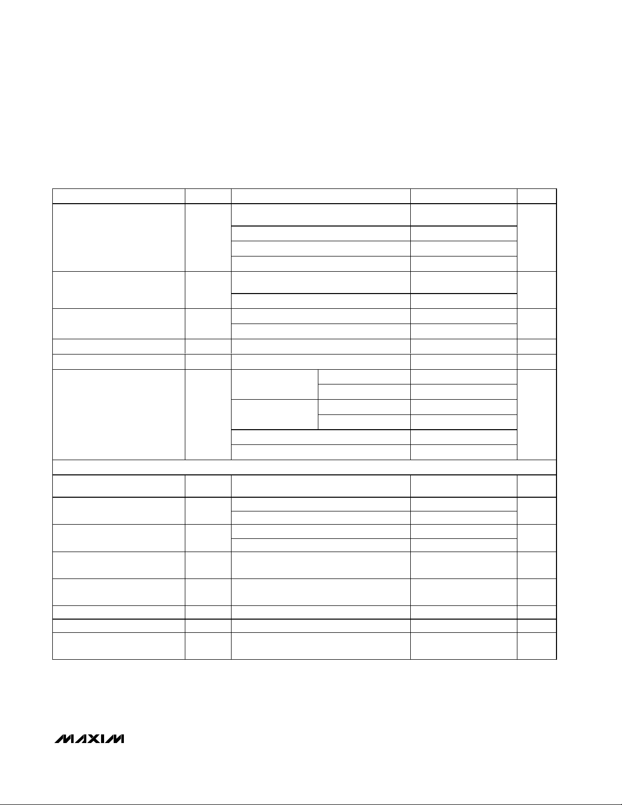
PARAMETER
CONDITIONS
UNITS
STATIC PERFORMANCE
Resolution N 10 Bits
Integral Nonlinearity INL RL = 0
LSB
Differential Nonlinearity DNL Guaranteed monotonic, RL = 0
LSB
Offset Error V
OS
LSB
Internal reference (Note1)
Gain Error (See Also Gain Error
Definition Section)
GE
External reference
%FSR
Internal reference
Gain-Error Temperature Drift
External reference
ppm/°C
DYNAMIC PERFORMANCE
f
OUT
= 10MHz
78
f
OUT
= 20MHz 77
f
CLK
= 165MHz,
A
OUT
= -1dBFS
f
OUT
= 40MHz 73
f
OUT
= 10MHz 77
f
OUT
= 20MHz 77
f
CLK
= 100MHz,
A
OUT
= -1dBFS
f
OUT
= 30MHz 76
Spurious-Free Dynamic Range to
Nyquist
SFDR
f
CLK
= 25MHz,
A
OUT
= -1dBFS
f
OUT
= 1MHz 79
dBc
f
CLK
= 165MHz, f
OUT
= 10MHz,
A
OUT
= -1dBFS, span = 10MHz
83
f
CLK
= 100MHz, f
OUT
= 5MHz,
A
OUT
= -1dBFS, span = 4MHz
84
Spurious-Free Dynamic Range
Within a Window
SFDR
f
CLK
= 25MHz, f
OUT
= 1MHz,
A
OUT
= -1dBFS, span = 2MHz
82
dBc
MTPR
8 tones at 400kHz spacing, f
CLK
= 78MHz,
f
OUT
= 15MHz to 18.2MHz
74 dBc
Multitone Power Ratio to Nyquist
SYMBOL
MIN TYP MAX
-1.0 ±0.25 +1.0
-0.5 ±0.2 +0.5
-0.5 ±0.1 +0.5
-11.0 ±1.5 +6.8
-6.25 ±0.7 +4.10
±150
±100
69.4
Page 3
MAX5854
Dual, 10-Bit, 165Msps, Current-Output DAC
_______________________________________________________________________________________ 3
ELECTRICAL CHARACTERISTICS (continued)
(AVDD= DVDD= CVDD= 3V, AGND = DGND = CGND = 0, f
DAC
= 165Msps, differential clock, external reference, V
REF
= 1.2V,
I
FS
= 20mA, output amplitude = 0dB FS, differential output, TA= T
MIN
to T
MAX
, unless otherwise noted. TA≥ +25°C guaranteed by
production test. T
A
< +25°C guaranteed by design and characterization. Typical values are at TA= +25°C.)
PARAMETER
CONDITIONS
UNITS
Multitone Spurious-Free Dynamic
Range Within a Window
8 tones at 2.1M H z sp aci ng ,
f
C LK
= 165M H z, f
OU T
= 28.3M H z to 45.2M H z,
sp an = 50M H z
70 dBc
Adjacent Channel Power Ratio
with UMTS
ACLR
f
OUT
= 30.72MHz, RBW = 30kHz,
f
CLK
= 122.88MHz
dB
f
OUT
= 10MHz -76
f
OUT
= 20MHz -74
f
CLK
= 165MHz,
A
OUT
= -1dBFS
f
OUT
= 40MHz -71
f
OUT
= 10MHz -75
f
OUT
= 20MHz -74
f
CLK
= 100MHz,
A
OUT
= -1dBFS
f
OUT
= 30MHz -73
Total Harmonic Distortion to
Nyquist (2nd- Through 8th-Order
Harmonics Included)
THD
f
CLK
= 25MHz,
A
OUT
= -1dBFS
f
OUT
= 1MHz -76
dBc
Output Channel-to-Channel
Isolation
f
OUT
= 10MHz 90 dB
Channel-to-Channel Gain
Mismatch
f
OUT
= 10MHz, G[3:0] = 1000
dB
Channel-to-Channel Phase
Mismatch
f
OUT
= 10MHz
Degrees
f
C LK
= 165M Hz, f
OU T
= 10M H z, I
FS
= 20m A
f
CLK
= 165MHz, f
OUT
= 10MHz, I
FS
= 5mA 61
f
CLK
= 65MHz, f
OUT
= 10MHz, I
FS
= 20mA 62
Signal-to-Noise Ratio to Nyquist
SNR
f
CLK
= 65MHz, f
OUT
= 10MHz, I
FS
= 5mA 62
dB
Interleaved mode disabled, IDE = 0
Maximum DAC Conversion Rate
f
DAC
Interleaved mode enabled, IDE = 1
Msps
Glitch Impulse 5 pV-s
Output Settling Time t
S
To ±0.1% error band (Note 3) 12 ns
Output Rise Time 10% to 90% (Note 3) 2.2 ns
Output Fall Time 90% to 10% (Note 3) 2.2 ns
ANALOG OUTPUT
Full-Scale Output Current Range
I
FS
220mA
Output Voltage Compliance
Range
V
Output Leakage Current Shutdown or standby mode -5 +5 µA
REFERENCE
Internal-Reference Output
Voltage
V
REFO
REN = 0
V
SYMBOL
MIN TYP MAX
165 200
82.5 100
-1.00 +1.25
1.13 1.24 1.32
65.5
0.025
0.05
60.5
Page 4
MAX5854
Dual, 10-Bit, 165Msps, Current-Output DAC
4 _______________________________________________________________________________________
ELECTRICAL CHARACTERISTICS (continued)
(AVDD= DVDD= CVDD= 3V, AGND = DGND = CGND = 0, f
DAC
= 165Msps, differential clock, external reference, V
REF
= 1.2V,
I
FS
= 20mA, output amplitude = 0dB FS, differential output, TA= T
MIN
to T
MAX
, unless otherwise noted. TA≥ +25°C guaranteed by
production test. T
A
< +25°C guaranteed by design and characterization. Typical values are at TA= +25°C.)
PARAMETER
CONDITIONS
UNITS
Internal-Reference Supply
Rejection
AV
DD
varied from 2.7V to 3.6V 0.5
mV/V
Internal-Reference OutputVoltage Temperature Drift
REN = 0
ppm/°C
Internal-Reference Output Drive
Capability
REN = 0 50 µA
External-Reference Input Voltage
Range
REN = 1
1.2
V
Current Gain
32
mA/mA
LOGIC INPUTS (DA9–DA0, DB9–DB0, CW)
Digital Input-Voltage High V
IH
0.65 x
V
Digital Input-Voltage Low V
IL
0.3 x
V
Digital Input Current I
IN
-1 +1 µA
Digital Input Capacitance C
IN
3pF
SINGLE-ENDED CLOCK INPUT/OUTPUT AND DCE INPUT (CLK, DCE)
Digital Input-Voltage High V
IH
DCE = 1
0.65 x
V
Digital Input-Voltage Low V
IL
DCE = 1
0.3 x
V
Digital Input Current I
IN
DCE = 1 -1 +1 µA
Digital Input Capacitance C
IN
DCE = 1 3 pF
Digital Output-Voltage High V
OH
DCE = 0, I
SOURCE
= 0.5mA, Figure 1
V
Digital Output-Voltage Low V
OL
DCE = 0, I
SINK
= 0.5mA, Figure 1
0.1 x
V
DIFFERENTIAL CLOCK INPUTS (CLKXP/CLKXN)
Differential Clock Input Internal
Bias
V
Differential Clock Input Swing 0.5 V
Clock Input Impedance Measured single ended 5 kΩ
POWER REQUIREMENTS
Analog Power-Supply Voltage AV
DD
2.7 3 3.6 V
Digital Power-Supply Voltage DV
DD
2.7 3 3.6 V
Clock Power-Supply Voltage CV
DD
2.7 3 3.6 V
SYMBOL
MIN TYP MAX
TCV
REFO
IFS/I
REF
±50
0.10
DV
DD
CV
DD
0.9 x
CV
DD
1.32
DV
DD
CV
DD
CV
DD
CVDD/2
Page 5
MAX5854
Dual, 10-Bit, 165Msps, Current-Output DAC
_______________________________________________________________________________________ 5
ELECTRICAL CHARACTERISTICS (continued)
(AVDD= DVDD= CVDD= 3V, AGND = DGND = CGND = 0, f
DAC
= 165Msps, differential clock, external reference, V
REF
= 1.2V,
I
FS
= 20mA, output amplitude = 0dB FS, differential output, TA= T
MIN
to T
MAX
, unless otherwise noted. TA≥ +25°C guaranteed by
production test. T
A
< +25°C guaranteed by design and characterization. Typical values are at TA= +25°C.)
PARAMETER
CONDITIONS
UNITS
I
FS
= 20mA (Note 2), single-ended clock
mode
46
5
Analog Supply Current I
AVDD
I
FS
= 2mA (Note 2), differential clock mode 5
mA
I
FS
= 20mA (Note 2), single-ended clock
mode
6.2 7.5
Digital Supply Current I
DVDD
6.2
mA
Clock Supply Current I
CVDD
Differential clock mode (DCE = 0) (Note 2) 24
mA
Total Standby Current
I
AVDD
+ I
DVDD
+ I
CVDD
3.1 3.7 mA
Total Shutdown Current I
SHDNIAVDD
+ I
DVDD
+ I
CVDD
1µA
I
FS
= 20mA (Note 2)
Single-ended clock
mode (DCE = 1)
I
FS
= 2mA (Note 2) 75
I
FS
= 20mA (Note 2)
Differential clock
mode (DCE = 0)
I
FS
= 2mA (Note 2)
Standby 9.3
Total Power Dissipation P
TOT
Shutdown
mW
TIMING CHARACTERISTICS (Figure 5, Figure 6)
Propagation Delay 1
Clock
cycles
1.2
DAC Data to CLK Rise/Fall Setup
Time
t
DCS
Differential clock mode (DCE = 0) (Note 4) 2.7
ns
0.8
DAC Data to CLK Rise/Fall Hold
Time
t
DCH
Differential clock mode (DCE = 0) (Note 4)
ns
Control Word to CW Rise Setup
Time
t
CS
2.5 ns
Control Word to CW Rise Hold
Time
t
CW
2.5 ns
CW High Time t
CWH
5ns
CW Low Time t
CWL
5ns
DACEN = 1 to V
OUT
Stable Time
(Coming Out of Standby)
t
STB
3µs
SYMBOL
I
= 20mA (Note 2), differential clock mode 43.2
FS
I
= 2mA (Note 2), single-ended clock mode
FS
I
= 20mA (Note 2), differential clock mode
FS
Single-ended clock mode (DCE = 1) (Note 2) 13.7 16.5
I
STANDBY
Single-ended clock mode (DCE = 1) (Note 4)
Single-ended clock mode (DCE = 1) (Note 4)
MIN TYP MAX
43.2
190 210
220
106
11.1
0.003
-0.5
Page 6
MAX5854
Dual, 10-Bit, 165Msps, Current-Output DAC
6 _______________________________________________________________________________________
ELECTRICAL CHARACTERISTICS (continued)
(AVDD= DVDD= CVDD= 3V, AGND = DGND = CGND = 0, f
DAC
= 165Msps, differential clock, external reference, V
REF
= 1.2V,
I
FS
= 20mA, output amplitude = 0dB FS, differential output, TA= T
MIN
to T
MAX
, unless otherwise noted. TA≥ +25°C guaranteed by
production test. T
A
< +25°C guaranteed by design and characterization. Typical values are at TA= +25°C.)
PARAMETER
SYMBOL
CONDITIONS
MIN
TYP
MAX
UNITS
PD = 0 to V
OUT
Stable Time
(Coming Out of Power-Down)
t
SHDN
µs
Maximum Clock Frequency at
CLKXP/CLKXN Input
f
CLK
MHz
Clock High Time t
CXH
CLKXP or CLKXN input 1.5 ns
Clock Low Time t
CXL
CLKXP or CLKXN input 1.5 ns
CLKXP Rise to CLK Output Rise
Delay
t
CDH
DCE = 0 2.7 ns
CLKXP Fall to CLK Output Fall
Delay
t
CDL
DCE = 0 2.7 ns
Note 1: Including the internal reference voltage tolerance and reference amplifier offset.
Note 2: f
DAC
= 165Msps, f
OUT
= 10MHz.
Note 3: Measured single-ended with 50Ω load and complementary output connected to AGND.
Note 4: Guaranteed by design, not production tested.
TO OUTPUT
PIN
5pF
0.5mA
0.5mA
1.6V
Figure 1. Load Test Circuit for CLK Outputs
500
165 200
Page 7
MAX5854
Dual, 10-Bit, 165Msps, Current-Output DAC
_______________________________________________________________________________________ 7
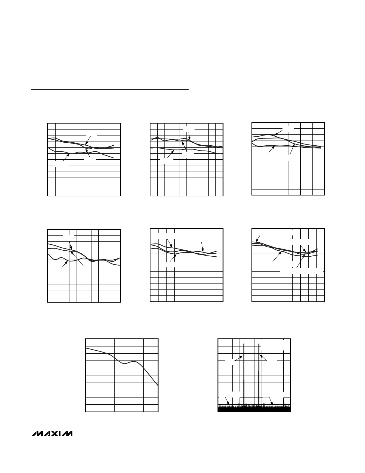
SPURIOUS-FREE DYNAMIC RANGE
vs. OUTPUT FREQUENCY (f
CLK
= 165MHz)
MAX5854 toc01
f
OUT
(MHz)
SFDR (dBc)
807050 6020 30 4010
35
40
45
50
55
60
65
70
75
80
85
90
30
090
0dBFS
-6dBFS
-12dBFS
SPURIOUS-FREE DYNAMIC RANGE
vs. OUTPUT FREQUENCY (f
CLK
= 100MHz)
MAX5854 toc02
f
OUT
(MHz)
SFDR (dBc)
403525 3010 15 205
35
40
45
50
55
60
65
70
75
80
85
90
30
045
50
0dBFS
-6dBFS
-12dBFS
SPURIOUS-FREE DYNAMIC RANGE
vs. OUTPUT FREQUENCY (f
CLK
= 25MHz)
MAX5854 toc03
f
OUT
(MHz)
SFDR (dBc)
119753
35
40
45
50
55
60
65
70
75
80
85
90
30
113
0dBFS
-6dBFS
-12dBFS
SPURIOUS-FREE DYNAMIC RANGE
vs. OUTPUT FREQUENCY (f
CLK
= 200MHz)
MAX5854 toc04
f
OUT
(MHz)
SFDR (dBc)
908060 7020 30 40 5010
35
40
45
50
55
60
65
70
75
80
85
90
30
0 100
0dBFS
-6dBFS
-12dBFS
SPURIOUS-FREE DYNAMIC RANGE
vs. OUTPUT FREQUENCY (f
CLK
= 165MHz)
MAX5854 toc05
f
OUT
(MHz)
SFDR (dBc)
807050 6020 30 4010
35
40
45
50
55
60
65
70
75
80
85
90
30
090
I
OUT
= 20mA
I
OUT
= 5mA
I
OUT
= 10mA
SPURIOUS-FREE DYNAMIC RANGE
vs. OUTPUT FREQUENCY (f
CLK
= 165MHz)
MAX5854 toc06
f
OUT
(MHz)
SFDR (dBc)
807050 6020 30 4010
35
40
45
50
55
60
65
70
75
80
85
90
30
090
AVDD = DVDD = CVDD = 3.3V
AVDD = DVDD = CVDD = 3.6V
AVDD = DVDD = CVDD = 2.7V
AVDD = DVDD = CVDD = 3V
SFDR vs. TEMPERATURE (f
CLK
= 165MHz,
f
OUT
= 10MHz, A
OUT
= 0dBFS)
MAX5854 toc07
TEMPERATURE (°C)
SFDR (dBc)
603510-15
75.5
76.0
76.5
77.0
77.5
78.0
78.5
79.0
79.5
80.0
75.0
-40 85
TWO-TONE INTERMODULATION DISTORTION
(f
CLK
= 165MHz, 1MHz WINDOW)
MAX5854 toc08
f
OUT
(MHz)
AMPLITUDE (dB)
5.45.35.1 5.24.7 4.8 4.9 5.04.6
-90
-80
-70
-60
-50
-40
-30
-20
-10
0
-100
4.5 5.5
2f
OUT2
- f
OUT1
f
OUT1
f
OUT2
2f
OUT1
- f
OUT2
f
OUT1
= 4.8541MHz
f
OUT2
= 5.0555MHz
Typical Operating Characteristics
(AVDD= DVDD= CVDD= 3V, AGND = DGND = CGND = 0, external reference, differential clock, IFS= 20mA, differential output, TA=
+25°C, unless otherwise noted.)
Page 8

MAX5854
Dual, 10-Bit, 165Msps, Current-Output DAC
8 _______________________________________________________________________________________
Typical Operating Characteristics (continued)
(AVDD= DVDD= CVDD= 3V, AGND = DGND = CGND = 0, external reference, differential clock, IFS= 20mA, differential output, TA=
+25°C, unless otherwise noted.)
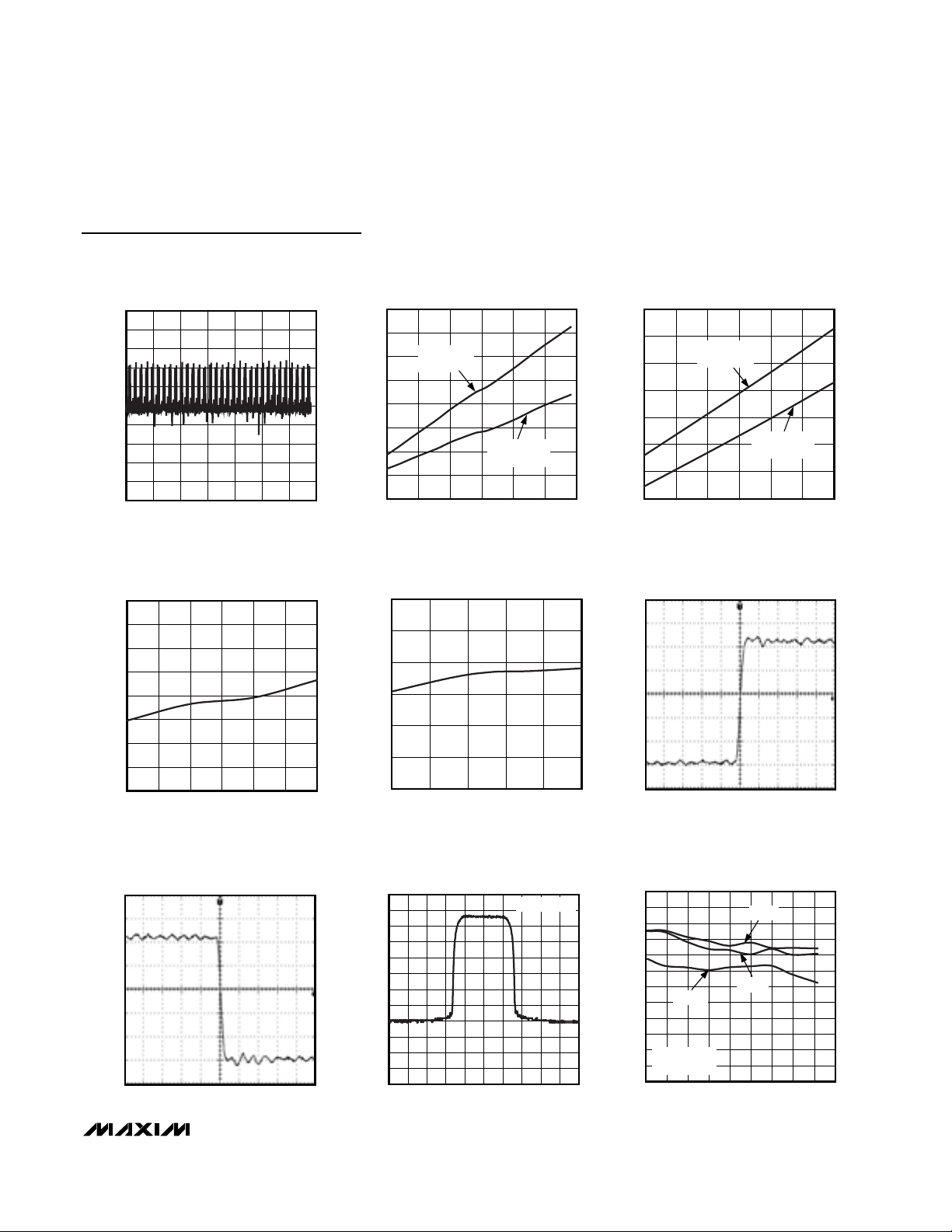
SINGLE-TONE SFDR
(f
CLK
= 165MHz, 10MHz WINDOW)
MAX5854 toc10
f
OUT
(MHz)
AMPLITUDE (dB)
8
7
56
-90
-80
-70
-60
-50
-40
-30
-20
-10
0
-100
412
f
OUT1
= 9.1040MHz
A
OUT
= -1dBFS
14
13
11
10
9
SINGLE-TONE SFDR
(f
CLK
= 100MHz, 4MHz WINDOW)
MAX5854 toc11
f
OUT
(MHz)
AMPLITUDE (dB)
4.5
3.5 4.0
-90
-80
-70
-60
-50
-40
-30
-20
-10
0
-100
3.0 6.5
f
OUT1
= 5.0533MHz
A
OUT
= -1dBFS
7.0
6.0
5.5
5.0
SINGLE-TONE SFDR
(f
CLK
= 25MHz, 2MHz WINDOW)
MAX5854 toc12
f
OUT
(MHz)
AMPLITUDE (dB)
0.9
0.4 0.6
-90
-80
-70
-60
-50
-40
-30
-20
-10
0
-100
0.1 1.6
f
OUT
= 1.0152MHz
A
OUT
= -1dBFS
1.9
1.4
1.1
SINGLE-TONE SFDR
(f
CLK
= 78MHz, 20MHz WINDOW)
MAX5854 toc13
f
OUT
(MHz)
AMPLITUDE (dB)
9.0
5.0
-90
-80
-70
-60
-50
-40
-30
-20
-10
0
-100
1.0 17.0
f
OUT
= 11.0333MHz
A
OUT
= -1dBFS
21.0
13.0
SINGLE-TONE FFT PLOT (f
CLK
= 165MHz,
f
OUT
= 10MHz, A
OUT
= 0dBFS, NYQUIST WINDOW)
MAX5854 toc14
f
OUT
(MHz)
AMPLITUDE (dB)
8.2MHz/div
-90
-80
-70
-60
-50
-40
-30
-20
-10
0
-100
0.5
82.5
INTEGRAL NONLINEARITY
vs. DIGITAL INPUT CODE
MAX5854 toc15
DIGITAL INPUT CODE
INL (LSB)
900750450 600300150
-0.4
-0.3
-0.2
-0.1
0
0.1
0.2
0.3
0.4
0.5
-0.5
0 1050
8-TONE SFDR PLOT
(f
CLK
= 165MHz, 35MHz WINDOW)
MAX5854 toc09
f
OUT
(MHz)
AMPLITUDE (dB)
24.7
19.7
9.7 14.7
-90
-80
-70
-60
-50
-40
-30
-20
-10
0
-100
4.7 29.7
39.7
34.7
f
T4
f
T3
f
T2
f
T1
f
T5
f
T6
f
T7
f
T8
fT1 = 17.493MHz
f
T2
= 18.997MHz
f
T3
= 20.200MHz
f
T4
= 21.253MHz
f
T5
= 24.035MHz
f
T6
= 25.087MHz
f
T7
= 26.741MHz
f
T8
= 27.869MHz
Page 9
MAX5854
Dual, 10-Bit, 165Msps, Current-Output DAC
_______________________________________________________________________________________ 9
Typical Operating Characteristics (continued)
(AVDD= DVDD= CVDD= 3V, AGND = DGND = CGND = 0, external reference, differential clock, IFS= 20mA, differential output, TA=
+25°C, unless otherwise noted.)
DIFFERENTIAL NONLINEARITY
vs. DIGITAL INPUT CODE
MAX5854 toc16
DIGITAL INPUT CODE
DNL (LSB)
900750450 600300150
-0.4
-0.3
-0.2
-0.1
0
0.1
0.2
0.3
0.4
0.5
-0.5
0 1050
POWER DISSIPATION vs. CLOCK FREQUENCY
(f
OUT
= 10MHz, A
OUT
= 0dBFS)
MAX5854 toc17
f
CLK
(MHz)
POWER DISSIPATION (mV)
14512045 70 95
160
170
180
190
200
210
220
230
150
20 170
DIFFERENTIAL
CLOCK DRIVE
SINGLE-ENDED
CLOCK DRIVE
POWER DISSIPATION vs. SUPPLY VOLTAGES
(f
CLK
= 165MHz, f
OUT
= 10MHz)
MAX5854 toc18
SUPPLY VOLTAGES (V)
POWER DISSIPATION (mW)
3.453.302.85 3.00 3.15
160
180
200
220
240
260
280
300
160
2.70 3.60
DIFFERENTIAL
CLOCK DRIVE
SINGLE-ENDED
CLOCK DRIVE
REFERENCE VOLTAGE vs. SUPPLY VOLTAGES
(f
CLK
= 165MHz, f
OUT
= 10MHz)
MAX5854 toc19
SUPPLY VOLTAGES (V)
REFEENCE VOLTAGE (V)
3.453.302.85 3.00 3.15
1.22160
1.22170
1.22180
1.22190
1.22200
1.22230
1.22230
1.22230
1.22150
2.70 3.60
REFERENCE VOLTAGE vs. TEMPERATURE
MAX5854 toc20
TEMPERATURE (°C)
REFERENCE VOLTAGE (V)
603510-15
1.20
1.21
1.22
1.23
1.24
1.25
1.19
-40 85
10ns/div
DYNAMIC RESPONSE RISE TIME
100mV/div
MAX5854 toc21
10ns/div
DYNAMIC RESPONSE FALL TIME
100mV/div
MAX5854 toc22
ACLR PLOT
(f
CLK
= 122.88MHz, f
OUT
= 30.72MHz)
MAX5854 toc23
1.468MHz/div
AMPLITUDE (dB)
-130
-120
-110
-100
-90
-80
-70
-60
-50
-40
-30
-20
-140
ACLR = 65.5dB
f
OUT
(MHz)
23.38 38.06
SPURIOUS-FREE DYNAMIC RANGE
vs. OUTPUT FREQUENCY (f
CLK
= 165MHz)
MAX5854 toc24
f
OUT
(MHz)
SFDR (dBc)
807050 6020 30 4010
35
40
45
50
55
60
65
70
75
80
85
90
30
090
0dBFS
-6dBFS
-12dBFS
SINGLE-ENDED
CLOCK DRIVE
Page 10

MAX5854
Dual, 10-Bit, 165Msps, Current-Output DAC
10 ______________________________________________________________________________________
Pin Description
PIN NAME FUNCTION
1 DA9/PD Channel A Input Data Bit 9 (MSB)/Power-Down
2
Channel A Input Data Bit 8/DAC Enable Control
3 DA7/IDE Channel A Input Data Bit 7/Interleaved Data Enable
4
Channel A Input Data Bit 6/Reference Enable. Setting REN = 0 enables the internal reference. Setting
REN = 1 disables the internal reference.
5 DA5/G3 Channel A Input Data Bit 5/Channel A Gain Adjustment Bit 3
6 DA4/G2 Channel A Input Data Bit 4/Channel A Gain Adjustment Bit 2
7 DA3/G1 Channel A Input Data Bit 3/Channel A Gain Adjustment Bit 1
8 DA2/G0 Channel A Input Data Bit 2/Channel A Gain Adjustment Bit 0
9 DA1 Channel A Input Data Bit 1
10 DA0 Channel A Input Data Bit 0 (LSB)
11 DB9 Channel B Input Data Bit 9 (MSB)
12 DB8 Channel B Input Data Bit 8
13 DB7 Channel B Input Data Bit 7
14 DB6 Channel B Input Data Bit 6
15 DB5 Channel B Input Data Bit 5
16 DV
DD
D i g i tal P ow er Inp ut. S ee the P ow er S up p l i es, Byp assi ng , D ecoup l i ng , and Layout secti on for m or e d etai l s.
17 DGND Digital Ground
18 DB4 Channel B Input Data Bit 4
19 DB3 Channel B Input Data Bit 3
20 DB2 Channel B Input Data Bit 2
21 DB1 Channel B Input Data Bit 1
22 DB0 Channel B Input Data Bit 0 (LSB)
23 CW Active-Low Control Word Write Pulse. The control word is latched on the rising edge of CW.
24 DCE
Active-Low Differential Clock Enable Input. Drive DCE low to enable the differential clock inputs
CLKXP and CLKXN. Drive DCE high to disable the differential clock inputs and enable the single-
ended CLK input.
25 CLKXP
Positive Differential Clock Input. With DCE = 0, CLKXP and CLKXN are enabled. With DCE = 1, CLKXP
and CLKXN are disabled. Connect CLKXP to CGND when the differential clock is disabled.
26 CLKXN
Negative Differential Clock Input. With DCE = 0, CLKXP and CLKXN are enabled. With DCE = 1, CLKXP
and CLKXN are disabled. Connect CLKXN to CV
DD
when the differential clock is disabled.
27, 30 CV
DD
Clock Power Input. See the Power Supplies, Bypassing, Decoupling, and Layout section for more
28 CLK
Single-Ended Clock Input/Output. With the differential clock disabled (DCE = 1), CLK becomes a
single-ended conversion clock input. With the differential clock enabled (DCE = 0), CLK is a single-
ended output that mirrors the differential clock inputs CLKXP and CLKXN. See the Clock Modes section
for more information on CLK.
29 CGND Clock Ground
31 REFO
Reference Input/Output. REFO serves as a reference input when the internal reference is disabled. If the
internal 1.24V reference is enabled, REFO serves as an output for the internal reference. When the
internal reference is enabled, bypass REFO to AGND with a 0.1µF capacitor
DA8/DACEN
DA6/REN
Page 11

Detailed Description
The MAX5854 dual, high-speed, 10-bit, current-output
DAC provides superior performance in communication
systems requiring low-distortion analog-signal reconstruction. The MAX5854 combines two DACs and an onchip 1.24V reference (Figure 2). The current outputs of
the DACs can be configured for differential or singleended operation. The full-scale output current range is
adjustable from 2mA to 20mA to optimize power dissipation and gain control.
The MAX5854 accepts an input data and a DAC conversion rate of 165MHz. The inputs are latched on the
rising edge of the clock whereas the output latches on
the following rising edge.
The MAX5854 features three modes of operation: normal,
standby, and power-down (Table 2). These modes allow
efficient power management. In power-down, the
MAX5854 consumes only 1µA of supply current. Wake-up
time from standby mode to normal DAC operation is 3µs.
Programming the DAC
An 8-bit control word routed through channel A’s data
port programs the gain matching, reference, and the
operational mode of the MAX5854. The control word is
latched on the rising edge of CW. CW is independent
of the DAC clock. The DAC clock can always remain
running, when the control word is written to the DAC.
Table 1 and Table 2 represent the control word format
and function.
The gain on channel A can be adjusted to achieve gain
matching between two channels in a user’s system.
The gain on channel A can be adjusted from -0.4dB to
0.35dB in steps of 0.05dB by using bits G3 to G0 (see
Table 3).
MAX5854
Dual, 10-Bit, 165Msps, Current-Output DAC
______________________________________________________________________________________ 11
Pin Description (continued)
PIN NAME FUNCTION
32 REFR
Full-Scale Current Adjustment. To set the output full-scale current, connect an external resistor RSET
between REFR and AGND. The output full-scale current is equal to 32 x V
REFO/RSET
.
33, 39 AV
DD
Anal og P ow er Inp ut. S ee the P ow er S up p l i es, Byp assi ng , D ecoup l i ng , and Layout secti on for m or e d etai l s.
34 OUTNB Channel B Negative Analog Current Output
35 OUTPB Channel B Positive Analog Current Output
36, 40 AGND Analog Ground
37 OUTNA Channel A Negative Analog Current Output
38 OUTPA Channel A Positive Analog Current Output
— EP Exposed Paddle. Connect EP to the common point of all ground planes.
Figure 2. Simplified Diagram
DV
DD
DGND
CW
DA0
DA1
DA2/G0
DA3/G1
DA4/G2
DA5/G3
DA6/REN
DA7/IDE
DA8/DACEN
DA9/PD
DB0
DB1
DB2
DB3
DB4
DB5
DB6
DB7
DB8
DB9
DCE
CLKXP
CLKXN
CLK
CV
DD
CGND
DIGITAL
POWER
MANAGEMENT
MAX5854
10-BIT
DACA
CONTROL WORD
DACA INPUT REGISTER
INPUT DATA
INTERLEAVER
DACB INPUT REGISTER
DISTRIBUTION
POWER
MANAGEMENT
CLOCK
CLOCK
CHANNEL A
GAIN
CONTROL
OPERATING
MODE
CONTROLLER
10-BIT
DACB
ANALOG
POWER
MANAGEMENT
IDE
1.24V REFERENCE
AND CONTROL
AMPLIFIER
REN
G0
G1
G2
G3
DACEN
PD
OUTPA
OUTNA
OUTPB
OUTNB
REFO
REFR
AV
AGND
AGND
DD
R
SET
Page 12

MAX5854
Dual, 10-Bit, 165Msps, Current-Output DAC
12 ______________________________________________________________________________________
Device Power-Up and
States of Operation
At power-up, the MAX5854’s default configuration is
internal reference noninterleaved input mode with a gain
of 0dB and a fully operational converter. In shutdown,
the MAX5854 consumes only 1µA of supply current, and
in standby the current consumption is 3.1mA. Wake-up
time from standby mode to normal operation is 3µs.
Clock Modes
The MAX5854 allows both single-ended CMOS and differential clock mode operation, and supports update
rates of up to 165Msps. These modes are selected
through an active-low control line called DCE. In singleended clock mode (DCE = 1), the CLK pin functions as
an input, which accepts a user-provided single-ended
clock signal. Data is written to the converter on the rising
edge of the clock. The DAC outputs (previous data) are
updated simultaneously on the same edge.
If the DCE pin is pulled low, the MAX5854 will operate in
differential clock mode. In this mode, the clock signal has
to be applied to differential clock input pins
CLKXP/CLKXN. The differential input accepts an input
range of ≥0.5V
P-P
and a common-mode range of 1V to
(CVDD- 0.5V), making the part ideal for low- input amplitude clock drives. CLKXP/CLKXN also help to minimize
the jitter, and allow the user to connect a crystal oscillator
directly to MAX5854.
MSB LSB
PD DACEN IDE REN G3 G2 G1 G0 X X
CONTROL WORD
FUNCTION
PD Power-Down. The part enters power-down mode if PD = 1.
DACEN DAC Enable. When DACEN = 0 and PD = 0, the part enters standby mode.
IDE
Interleaved Data Mode. IDE = 1 enables the interleaved data mode. In this mode, digital data for both
channels is applied through channel A in a multiplexed fashion. Channel B data is written on the falling edge
of the clock signal and channel A data is written on the rising edge of the clock signal.
REN
Reference Enable Bit. REN = 0 activates the internal reference. REN = 1 disables the internal reference and
requires the user to apply an external reference between 0.1V to 1.32V.
G3 Bit 3 (MSB) of Gain Adjust Word
G2 Bit 2 of Gain Adjust Word
G1 Bit 1 of Gain Adjust Word
G0 Bit 0 (LSB) of Gain Adjust Word
Table 1. Control Word Format and Function
MODE
REN
Normal operation;
noninterleaved inputs;
internal reference active
01
0
Normal operation;
noninterleaved inputs;
internal reference disabled
01
1
Normal operation;
interleaved inputs; internal
reference disabled
01
1
Standby 0 0
X
Power-down 1 X
X
Power-up 0 1
X
Table 2. Configuration Modes
GAIN ADJUSTMENT ON
CHANNEL A (dB)
G3G2G1
G0
+0.4 0000
0 1000
-0.35 1111
Table 3. Gain Difference Setting
X = Don’t care.
PD DACEN IDE
0
0
1
X
X
X
Page 13

MAX5854
Dual, 10-Bit, 165Msps, Current-Output DAC
______________________________________________________________________________________ 13
The CLK pin now becomes an output, and provides a
single-ended replica of the differential clock signal,
which may be used to synchronize the input data. Data is
written to the device on the rising edge of the CLK signal.
Internal Reference and Control Amplifier
The MAX5854 provides an integrated 50ppm/°C, 1.24V,
low-noise bandgap reference that can be disabled and
overridden with an external reference voltage. REFO
serves either as an external reference input or an integrated reference output. If REN =0, the internal reference is selected and REFO provides a 1.24V (50µA)
output. Buffer REFO with an external amplifier, when
driving a heavy load.
The MAX5854 also employs a control amplifier
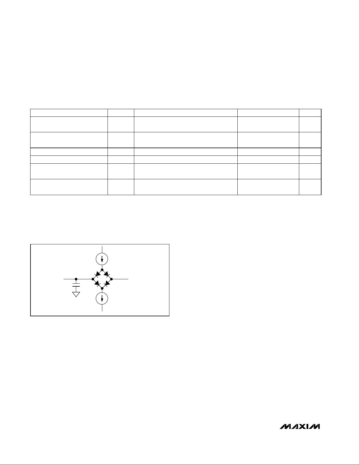
designed to simultaneously regulate the full-scale output current (I
FS
) for both outputs of the devices.
Calculate the output current as:
I
FS
= 32 ✕ I
REF
where I
REF
is the reference output current (I
REF
=
V
REFO
/ R
SET
) and IFSis the full-scale output current.
R
SET
is the reference resistor that determines the
amplifier output current of the MAX5854 (Figure 3). This
current is mirrored into the current-source array where
IFSis equally distributed between matched current segments and summed to valid output current readings for
the DACs.
External Reference
To disable the internal reference of the MAX5854, set
REN = 1. Apply a temperature-stable, external reference
to drive the REFO pin and set the full-scale output
(Figure 4). For improved accuracy and drift performance, choose a fixed output voltage reference such as
the 1.2V, 25ppm/°C MAX6520 bandgap reference.
Detailed Timing
The MAX5854 accepts an input data and the DAC conversion rate of up to 165Msps. The input latches on the
rising edge of the clock, whereas the output latches on
the following rising edge.
Figure 5 depicts the write cycle of the two DACs in noninterleaved mode.
The MAX5854 can also operate in an interleaved data
mode. Programming the IDE bit with a high level activates
this mode (Tables 1 and 2). In interleaved mode, data for
both DAC channels is written through input port A.
Channel B data is written on the falling edge of the clock
signal and then channel A data is written on the following
rising edge of the clock signal. Both DAC outputs (channel A and B) are updated simultaneously on the next following rising edge of the clock. In interleaved data mode,
the maximum input data rate per channel is half of the
rate in noninterleaved mode. The interleaved data mode
is attractive for applications where lower data rates are
acceptable and interfacing on a single 10-bit bus is
desired (Figure 6).
I
FS
C
COMP
*
REFR
I
REF
REFO
MAX4040
1.24V
BANDGAP
REFERENCE
CURRENT-
SOURCE
ARRAY
*COMPENSATION CAPACITOR (C
COMP
≈ 100nF).
OPTIONAL EXTERNAL BUFFER
FOR HEAVIER LOADS
MAX5854
I
REF
=
V
REF
R
SET
R
SET
AGND
AGND
REN = 0
Figure 3. Setting IFSwith the Internal 1.24V Reference and the
Control Amplifier
AV
DD
EXTERNAL
1.2V
REFERENCE
MAX6520
AGND
0.1µF10µF
AV
DD
AGND
I
FS
REFR
I
REF
REFO
1.24V
BANDGAP
REFERENCE
CURRENT-
SOURCE
ARRAY
MAX5854
R
SET
AGND
REN = 1
Figure 4. MAX5854 with External Reference
Page 14

MAX5854
Dual, 10-Bit, 165Msps, Current-Output DAC
14 ______________________________________________________________________________________
CLKXN
CLKXP
CLK
OUTPUT
CW
DA0–DA9
OUTPA
OUTNA
DB0–DB9
OUTPB
OUTNB
DACA - 1
DACB - 1
DACA
DACB
DACA + 1
DACB + 1
DACA + 2
DACB + 2
CONTROL
WORD
XXXX
DACA + 3
DACB + 3
DACA - 1
DACB - 1
DACA
DACB
DACA + 1
DACB + 1
DACA + 2
DACB + 2
XXXX
(CONTROL WORD DATA)
XXXX
DACA + 3
DACB + 3
t
CXHtCXL
t
CDH
t
CDL
t
DCStDCH
t
DCStDCH
t
CWL
tCSt
CW
Figure 5. Timing Diagram for Noninterleaved Data Mode (IDE = 0)
CLKXN
CLKXP
CLK
OUTPUT
CW
DA0–DA9
OUTPA
OUTNA
OUTPB
OUTNB
t
CXL
t
CXH
t
CDH
t
CDL
t
DCStDCH
t
DCStDCH
tCSt
CW
t
CWL
DACA DACB + 1 DACA + 1
CONTROL
WORD
DACB + 2 DACA + 2
DACA - 1
DACB - 1
DACA
DACB
DACA + 1
DACB + 1
Figure 6. Timing Diagram for Interleaved Data Mode (IDE = 1)
Page 15

MAX5854
Dual, 10-Bit, 165Msps, Current-Output DAC
______________________________________________________________________________________ 15
Applications Information
Differential-to-Single-Ended Conversion
The MAX5854 exhibits excellent dynamic performance
to synthesize a wide variety of modulation schemes,
including high-order QAM modulation with OFDM.
Figure 7 shows a typical application circuit with output
transformers performing the required differential-to-single-ended signal conversion. In this configuration, the
MAX5854 operates in differential mode, which reduces
even-order harmonics, and increases the available output power.
Differential DC-Coupled Configuration
Figure 8 shows the MAX5854 output operating in differential, DC-coupled mode. This configuration can be
used in communications systems employing analog
quadrature upconverters and requiring a baseband
sampling, dual-channel, high-speed DAC for I/Q synthesis. In these applications, information bandwidth can
extend from 10MHz down to several hundred kilohertz.
DC-coupling is desirable to eliminate long discharge
time constants that are problematic with large, expensive
coupling capacitors. Analog quadrature upconverters
have a DC common-mode input requirement of typically
0.7V to 1.0V. The MAX5854 differential I/Q outputs can
maintain the desired full-scale level at the required 0.7V
to 1.0V DC common-mode level when powered from a
single 2.85V (±5%) supply. The MAX5854 meets this
low-power requirement with minimal reduction in dynamic range while eliminating the need for level-shifting
resistor networks.
Power Supplies, Bypassing,
Decoupling, and Layout
Grounding and power-supply decoupling strongly influence the MAX5854 performance. Unwanted digital
crosstalk can couple through the input, reference,
power-supply, and ground connections, which can
affect dynamic specifications, like signal-to-noise ratio
DA0–DA9
10
MAX5854
1/2
50Ω
100Ω
50Ω
OUTPA
OUTNA
V
OUTA
,
SINGLE ENDED
DB0–DB9
10
MAX5854
1/2
50Ω
100Ω
50Ω
OUTPB
OUTNB
V
OUTB
,
SINGLE ENDED
CV
DD
DV
DD
AV
DD
CGNDDGNDAGND
Figure 7. Application with Output Transformer Performing
Differential-to-Single-Ended Conversion
DA0–DA9
10
MAX5854
1/2
1/2
50Ω
50Ω
CV
DD
DV
DD
AV
DD
CGNDDGNDAGND
OUTPA
OUTNA
DB0–DB9
10
MAX5854
50Ω
50Ω
OUTPB
OUTNB
Figure 8. Application with DC-Coupled Differential Outputs
Page 16

MAX5854
Dual, 10-Bit, 165Msps, Current-Output DAC
16 ______________________________________________________________________________________
or spurious-free dynamic range. In addition, electromagnetic interference (EMI) can either couple into or
be generated by the MAX5854. Observe the grounding
and power-supply decoupling guidelines for highspeed, high-frequency applications. Follow the power
supply and filter configuration to realize optimum
dynamic performance.
Use of a multilayer printed circuit (PC) board with separate ground and power-supply planes is recommended. Run high-speed signals on lines directly above the
ground plane. The MAX5854 has separate analog and
digital ground buses (AGND, CGND, and DGND,
respectively). Provide separate analog, digital, and
clock ground sections on the PC board with only one
point connecting the three planes. The ground connection points should be located underneath the device
and connected to the exposed paddle. Run digital signals above the digital ground plane and analog/clock
signals above the analog/clock ground plane. Digital
signals should be kept away from sensitive analog,
clock, and reference inputs. Keep digital signal paths
short and metal trace lengths matched to avoid propagation delay and data skew mismatch.
The MAX5854 includes three separate power-supply
inputs: analog (AVDD), digital (DVDD), and clock
(CV
DD
). Use a single linear regulator power source to
branch out to three separate power-supply lines (AVDD,
DV
DD
, CVDD) and returns (AGND, DGND, CGND).
Filter each power-supply line to the respective return
line using LC filters comprising ferrite beads and 10µF
capacitors. Filter each supply input locally with 0.1µF
ceramic capacitors to the respective return lines.
Note: To maintain the dynamic performance of the
Electrical Characteristics, ensure the voltage difference between DV
DD
, AVDD, and CVDDdoes not
exceed 150mV.
Thermal Characteristics and Packaging
Thermal Resistance
40-lead thin QFN-EP:
θ
JA
= 38°C/W
The MAX5854 is packaged in a 40-pin thin QFN-EP
package, providing greater design flexibility, increased
thermal efficiency, and optimized AC performance of
the DAC. The EP enables the implementation of
grounding techniques, which are necessary to ensure
highest performance operation.
In this package, the data converter die is attached to
an EP leadframe with the back of this frame exposed at
the package bottom surface, facing the PC board side
of the package. This allows a solid attachment of the
package to the PC board with standard infrared (IR)
flow soldering techniques. A specially created land pattern on the PC board, matching the size of the EP
(4.1mm ✕ 4.1mm), ensures the proper attachment and
grounding of the DAC. Designing vias* into the land
area and implementing large ground planes in the PC
board design allows for highest performance operation
of the DAC. Use an array of 3
✕ 3 vias (≤0.3mm diame-
ter per via hole and 1.2mm pitch between via holes) for
this 40-pin thin QFN-EP package (package code:
T4066-1).
Dynamic Performance Parameter Definitions
Adjacent Channel Leakage Ratio (ACLR)
Commonly used in combination with wideband codedivision multiple-access (WCDMA), ACLR reflects the
leakage power ratio in dB between the measured
power within a channel relative to its adjacent channel.
ACLR provides a quantifiable method of determining
out-of-band spectral energy and its influence on an
adjacent channel when a bandwidth-limited RF signal
passes through a nonlinear device.
Total Harmonic Distortion (THD)
THD is the ratio of the RMS sum of all essential harmonics (within a Nyquist window) of the input signal to the
fundamental itself. This can be expressed as:
where V1is the fundamental amplitude, and V2through
VNare the amplitudes of the 2nd through Nth order harmonics. The MAX5854 uses the first seven harmonics
for this calculation.
Spurious-Free Dynamic Range (SFDR)
SFDR is the ratio of RMS amplitude of the carrier frequency (maximum signal component) to the RMS value
of their next-largest spectral component. SFDR is usually measured in dBc with respect to the carrier frequency amplitude or in dBFS with respect to the DAC’s
full-scale range. Depending on its test condition, SFDR
is observed within a predefined window or to Nyquist.
THD
VVV V
V
N
=×
++ +
log
... ...
20
2
2
3
2
4
22
1
*Vias connect the land pattern to internal or external copper planes.
Page 17
MAX5854
Dual, 10-Bit, 165Msps, Current-Output DAC
______________________________________________________________________________________ 17
Multitone Power Ratio (MTPR)
A series of equally spaced tones are applied to the DAC
with one tone removed from the center of the range.
MTPR is defined as the worst-case distortion (usually a
3rd-order harmonic product of the fundamental frequencies), which appears as the largest spur at the frequency
of the missing tone in the sequence. This test can be performed with any number of input tones; however, four and
eight tones are among the most common test conditions
for CDMA- and GSM/EDGE-type applications.
Intermodulation Distortion (IMD)
The two-tone IMD is the ratio expressed in dBc of either output tone to the worst 3rd-order (or higher) IMD products.
Static Performance Parameter Definitions
Integral Nonlinearity (INL)
Integral nonlinearity (INL) is the deviation of the values
on an actual transfer function from a line drawn
between the end points of the transfer function, once
offset and gain errors have been nullified. For a DAC,
the deviations are measured at every individual step.
Differential Nonlinearity (DNL)
Differential nonlinearity (DNL) is the difference between
an actual step height and the ideal value of 1 LSB. A
DNL error specification no more negative than -1 LSB
guarantees monotonic transfer function.
Offset Error
Offset error is the current flowing from positive DAC
output when the digital input code is set to zero. Offset
error is expressed in LSBs.
Gain Error
A gain error is the difference between the ideal and the
actual full-scale output current on the transfer curve,
after nullifying the offset error. This error alters the slope
of the transfer function and corresponds to the same
percentage error in each step. The ideal current is
defined by reference voltage at V
REFO
/ I
REF
x 32.
Settling Time
The settling time is the amount of time required from the
start of a transition until the DAC output settles to its
new output value to within the converter’s specified
accuracy.
Glitch Impulse
A glitch is generated when a DAC switches between
two codes. The largest glitch is usually generated
around the midscale transition, when the input pattern
transitions from 011…111 to 100…000. This occurs due
to timing variations between the bits. The glitch impulse
is found by integrating the voltage of the glitch at the
midscale transition over time. The glitch impulse is usually specified in pV-s.
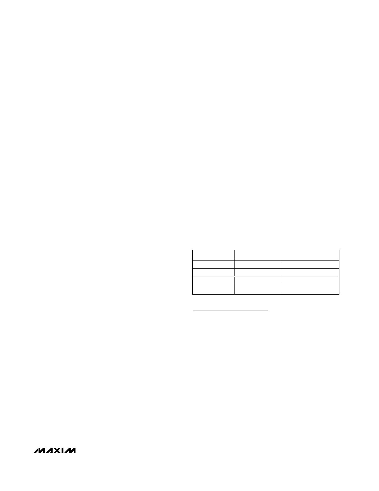
PART
RESOLUTION
MAX5851 80 8-bit, dual
MAX5852 165 8-bit, dual
MAX5853 80 10-bit, dual
MAX5854 165 10-bit, dual
Table 4. Part Selection Table
Chip Information
TRANSISTOR COUNT: 9,035
PROCESS: CMOS
SPEED (Msps)
Page 18

MAX5854
Dual, 10-Bit, 165Msps, Current-Output DAC
Maxim cannot assume responsibility for use of any circuitry other than circuitry entirely embodied in a Maxim product. No circuit patent licenses are
implied. Maxim reserves the right to change the circuitry and specifications without notice at any time.
18 ____________________Maxim Integrated Products, 120 San Gabriel Drive, Sunnyvale, CA 94086 408-737-7600
© 2004 Maxim Integrated Products Printed USA is a registered trademark of Maxim Integrated Products.
Package Information
(The package drawing(s) in this data sheet may not reflect the most current specifications. For the latest package outline information,
go to www.maxim-ic.com/packages
.)
Package Information
(The package drawing(s) in this data sheet may not reflect the most current specifications. For the latest package outline information,
go to www.maxim-ic.com/packages
.)
Package Information
(The package drawing(s) in this data sheet may not reflect the most current specifications. For the latest package outline information,
go to www.maxim-ic.com/packages
.)
Package Information
(The package drawing(s) in this data sheet may not reflect the most current specifications. For the latest package outline information,
go to www.maxim-ic.com/packages
.)
QFN THIN 6x6x0.8.EPS
e e
LL
A1 A2
A
E/2
E
D/2
D
E2/2
E2
(NE-1) X e
(ND-1) X e
e
D2/2
D2
b
k
k
L
C
L
C
L
C
L
C
L
D
1
2
21-0141
PACKAGE OUTLINE
36,40L THIN QFN, 6x6x0.8 mm
8. COPLANARITY APPLIES TO THE EXPOSED HEAT SINK SLUG AS WELL AS THE TERMINALS.
6. ND AND NE REFER TO THE NUMBER OF TERMINALS ON EACH D AND E SIDE RESPECTIVELY.
5. DIMENSION b APPLIES TO METALLIZED TERMINAL AND IS MEASURED BETWEEN 0.25 mm AND 0.30 mm
FROM TERMINAL TIP.
4. THE TERMINAL #1 IDENTIFIER AND TERMINAL NUMBERING CONVENTION SHALL CONFORM TO JESD 95-1
SPP-012. DETAILS OF TERMINAL #1 IDENTIFIER ARE OPTIONAL, BUT MUST BE LOCATED WITHIN THE
ZONE INDICATED. THE TERMINAL #1 IDENTIFIER MAY BE EITHER A MOLD OR MARKED FEATURE.
9. DRAWING CONFORMS TO JEDEC MO220.
7. DEPOPULATION IS POSSIBLE IN A SYMMETRICAL FASHION.
3. N IS THE TOTAL NUMBER OF TERMINALS.
2. ALL DIMENSIONS ARE IN MILLIMETERS. ANGLES ARE IN DEGREES.
1. DIMENSIONING & TOLERANCING CONFORM TO ASME Y14.5M-1994.
NOTES:
10. WARPAGE SHALL NOT EXCEED 0.10 mm.
D
2
2
21-0141
PACKAGE OUTLINE
36, 40L THIN QFN, 6x6x0.8 mm
 Loading...