

Page 1
General Description
The MAX5811 is a single, 10-bit voltage-output digital-toanalog converter (DAC) with an I2C™-compatible 2-wire
interface that operates at clock rates up to 400kHz. The
device operates from a single 2.7V to 5.5V supply and
draws only 100µA at VDD= 3.6V. A low-power powerdown mode decreases current consumption to less than
1µA. The MAX5811 features three software-selectable
power-down output impedances: 100kΩ, 1kΩ, and high
impedance. Other features include an internal precision
Rail-to-Rail®output buffer and a power-on reset (POR)
circuit that powers up the DAC in the 100kΩ power-down
mode.
The MAX5811 features a double-buffered I2C-compatible
serial interface that allows multiple devices to share a single bus. All logic inputs are CMOS-logic compatible and
buffered with Schmitt triggers, allowing direct interfacing
to optocoupled and transformer-isolated interfaces. The
MAX5811 minimizes digital noise feedthrough by disconnecting the clock (SCL) signal from the rest of the device
when an address mismatch is detected.
The MAX5811 is specified over the extended temperature
range of -40°C to +85°C and is available in a space-saving 6-pin SOT23 package. Refer to the MAX5812 data
sheet for the 12-bit version.
Applications
Digital Gain and Offset Adjustments
Programmable Voltage and Current Sources
Programmable Attenuation
VCO/Varactor Diode Control
Low-Cost Instrumentation
Battery-Operated Equipment
Features
♦ Ultra-Low Supply Current
100µA at V
DD
= 3.6V
130µA at VDD= 5.5V
♦ 300nA Low-Power Power-Down Mode
♦ Single 2.7V to 5.5V Supply Voltage
♦ Fast 400kHz I
2
C-Compatible 2-Wire Serial
Interface
♦ Schmitt-Trigger Inputs for Direct Interfacing
to Optocouplers
♦ Rail-to-Rail Output Buffer Amplifier
♦ Three Software-Selectable Power-Down Output
Impedances
100kΩ, 1kΩ, and High Impedance
♦ Read-Back Mode for Bus and Data Checking
♦ Power-On Reset to Zero
♦ Miniature 6-Pin SOT23 Package
MAX5811
10-Bit, Low-Power, 2-Wire Interface, Serial,
Voltage-Output DAC
________________________________________________________________ Maxim Integrated Products 1
SCL
SDA
1
2
6
5
V
DD
ADD
GND
OUT
MAX5811
SOT23
TOP VIEW
3
4
Pin Configuration
Ordering Information
R
S
R
S
R
S
R
S
R
P
R
P
V
DD
µC
SDA
SCL
SDA
SDA
SCL
SCL
V
DD
V
DD
V
DD
OUT
OUT
MAX5811
MAX5811
Typical Operating Circuit
19-2270; Rev 1; 11/04
For pricing, delivery, and ordering information, please contact Maxim/Dallas Direct! at
1-888-629-4642, or visit Maxim’s website at www.maxim-ic.com.
PART
TEMP RANGE
PIN-
TOP
MARK
MAX5811LEUT-T
6 SOT23-6
AAYS
MAX5811MEUT-T
6 SOT23-6
AAYU
MAX5811NEUT-T
6 SOT23-6
AAYW
MAX5811PEUT-T
6 SOT23-6
AAYY
Functional Diagram appears at end of data sheet.
Rail-to-Rail is a registered trademark of Nippon Motorola, Ltd.
I
2
C is a trademark of Philips Corp.
PACKAGE
-40°C to +85°C
-40°C to +85°C
-40°C to +85°C
-40°C to +85°C
Page 2
MAX5811
10-Bit Low Power 2-Wire Interface Serial,
Voltage-Output DAC
2 _______________________________________________________________________________________
ABSOLUTE MAXIMUM RATINGS
ELECTRICAL CHARACTERISTICS
(VDD= +2.7V to +5.5V, GND = 0, RL= 5kΩ, CL= 200pF, TA= T
MIN
to T
MAX
, unless otherwise noted. Typical values are at
V
DD
= +5V, TA= +25°C.) (Note 1)
Stresses beyond those listed under “Absolute Maximum Ratings” may cause permanent damage to the device. These are stress ratings only, and functional
operation of the device at these or any other conditions beyond those indicated in the operational sections of the specifications is not implied. Exposure to
absolute maximum rating conditions for extended periods may affect device reliability.
VDD, SCL, SDA to GND............................................-0.3V to +6V
OUT, ADD to GND........................................-0.3V to V
DD
+ 0.3V
Maximum Current into Any Pin............................................50mA
Continuous Power Dissipation (T
A
= +70°C)
6-Pin SOT23 (derate 9.1mW above +70°C).................727mW
Operating Temperature Range ...........................-40°C to +85°C
Maximum Junction Temperature .....................................+150°C
Storage Temperature Range .............................-65°C to +150°C
Lead Temperature (soldering, 10s) .................................+300°C
PARAMETER
SYMBOL
CONDITIONS
MIN
TYP
MAX
UNITS
STATIC ACCURACY (Note 2)
Resolution N 10
Bits
Integral Nonlinearity INL (Note 3)
±4
LSB
Differential Nonlinearity DNL Guaranteed monotonic (Note 3)
LSB
Zero-Code Error ZCE Code = 000 hex, VDD = 2.7V ±6
mV
Zero-Code Error Tempco 2.3
ppm/°C
Gain Error GE Code = 3FF hex
-3
%FS
Gain-Error Tempco
ppm/°C
DAC OUTPUT
Output Voltage Range No load (Note 4) 0
V
DC Output Impedance Code = 200 hex 1.2 Ω
VDD = 5V, V
OUT
= full scale (short to GND)
Short-Circuit Current
V
DD
= 3V, V
OUT
= full scale (short to GND)
mA
VDD = 5V 8
Wake-Up Time
V
DD
= 3V 8
µs
DAC Output Leakage Current
Power-down mode = high impedance,
V
DD
= 5.5V, V
OUT
= VDD or GND
±1 µA
DIGITAL INPUTS (SCL, SDA)
Input High Voltage V
IH
V
Input Low Voltage V
IL
V
Input Hysteresis
0.05 x
V
Input Leakage Current Digital inputs = 0 or V
DD
±1µA
Input Capacitance 6pF
DIGITAL OUTPUT (SDA)
Output Logic Low Voltage V
OL
I
SINK
= 3mA 0.4 V
Three-State Leakage Current I
L
Digital inputs = 0 or V
DD
±1µA
6pF
±0.5
±0.5
±40
0.7 x
V
DD
V
DD
-0.8
0.26
42.2
15.1
±0.1
±0.1
V
DD
0.3 x
V
DD
Three-State Output Capacitance
±0.1
Page 3
MAX5811
10-Bit Low Power 2-Wire Interface Serial,
Voltage-Output DAC
_______________________________________________________________________________________ 3
Note 1: All devices are 100% production tested at TA= +25°C and are guaranteed by design for TA= T
MIN
to T
MAX
.
Note 2: Static specifications are tested with the output unloaded.
Note 3: Linearity is guaranteed from codes 29 to 995.
Note 4: Offset and gain error limit the FSR.
Note 5: Guaranteed by design. Not production tested.
ELECTRICAL CHARACTERISTICS (continued)
(VDD= +2.7V to +5.5V, GND = 0, RL= 5kΩ, CL= 200pF, TA= T
MIN
to T
MAX
, unless otherwise noted. Typical values are at
V
DD
= +5V, TA= +25°C.) (Note 1)
PARAMETER
CONDITIONS
UNITS
DYNAMIC PERFORMANCE
Voltage-Output Slew Rate SR 0.5
V/µs
Voltage-Output Settling Time
To 1/2LSB code 100 hex to 300 hex or 300
hex to 100 hex (Note 5)
412µs
Digital Feedthrough
0.2
nV-s
Digital-to-Analog Glitch Impulse
Major-carry transition (code = 1FF hex to 200
hex and 200 hex to 1FF hex)
12
nV-s
POWER SUPPLIES
Supply Voltage Range V
DD
2.7 5.5 V
All digital inputs at 0 or VDD = 3.6V
Supply Current with
No Load
All digital inputs at 0 or V
DD
= 5.5V
Power-Down Supply Current All digital inputs at 0 or V
DD
= 5.5V 0.3 1 µA
TIMING CHARACTERISTICS (Figure 1)
Serial Clock Frequency f
SCL
0
kHz
Bus-Free Time Between STOP
and START Conditions
t
BUF
1.3 µs
START Condition Hold Time
0.6 µs
SCL Pulse Width Low t
LOW
1.3 µs
SCL Pulse Width High t
HIGH
0.6 µs
Repeated START Setup Time
0.6 µs
Data Hold Time
0 0.9 µs
Data Setup Time
ns
SDA and SCL Receiving
Rise Time
t
r
(Note 5) 0
ns
SDA and SCL Receiving
Fall Time
t
f
(Note 5) 0
ns
SDA Transmitting Fall Time t
f
(Note 5)
20 +
ns
STOP Condition Setup Time
0.6 µs
Bus Capacitance C
b
(Note 5)
pF
Maximum Duration of
Suppressed Pulse Widths
t
SP
050ns
SYMBOL
Code = 000 hex, digital inputs from 0 to V
t
HD,STA
t
SU,STA
t
HD,DAT
t
SU,DAT
t
SU,STO
DD
MIN TYP MAX
100 170
130 190
400
100
300
300
0.1C
b
250
400
Page 4
MAX5811
10-Bit Low Power 2-Wire Interface Serial,
Voltage-Output DAC
4 _______________________________________________________________________________________
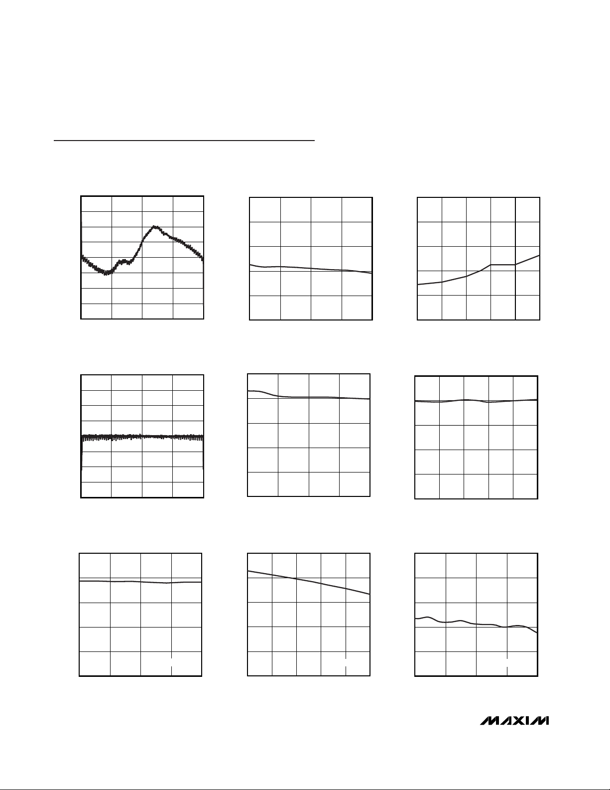
-1.00
-0.75
-0.50
-0.25
0
0.25
0.50
0.75
1.00
0 256 512 768 1024
INTEGRAL NONLINEARITY
vs. INPUT CODE
MAX5811 toc01
INPUT CODE
INTEGRAL NONLINEARITY (LSB)
0
0.25
0.75
0.50
1.00
1.25
INTEGRAL NONLINEARITY
vs. SUPPLY VOLTAGE
MAX5811 toc02
SUPPLY VOLTAGE (V)
INTEGRAL NONLINEARITY (LSB)
2.7 4.13.4 4.8 5.5
0
0.25
0.75
0.50
1.00
1.25
-40 10-15 35 60 85
INTEGRAL NONLINEARITY
vs. TEMPERATURE
MAX5811 toc03
TEMPERATURE (°C)
INTEGRAL NONLINEARITY (LSB)
-1.00
-0.75
-0.50
-0.25
0
0.25
0.50
0.75
1.00
0 256 512 768 1024
DIFFERENTIAL NONLINEARITY
vs. INPUT CODE
MAX5811 toc04
INPUT CODE
DIFFERENTIAL NONLINEARITY (LSB)
-0.5
-0.4
-0.2
-0.3
-0.1
0
DIFFERENTIAL NONLINEARITY
vs. SUPPLY VOLTAGE
MAX5811 toc05
SUPPLY VOLTAGE (V)
DIFFERENTIAL NONLINEARITY (LSB)
2.7 4.13.4 4.8 5.5
-0.5
-0.4
-0.2
-0.3
-0.1
0
-40 10-15 35 60 85
DIFFERENTIAL NONLINEARITY
vs. TEMPERATURE
MAX5811 toc06
TEMPERATURE (°C)
DIFFERENTIAL NONLINEARITY (LSB)
0
2
6
4
8
10
ZERO-CODE ERROR
vs. SUPPLY VOLTAGE
MAX8511 toc07
SUPPLY VOLTAGE (V)
ZERO-CODE ERROR (mV)
2.7 4.13.4 4.8 5.5
NO LOAD
0
2
6
4
8
10
-40 10-15 35 60 85
ZERO-CODE ERROR
vs. TEMPERATURE
MAX5811 toc08
TEMPERATURE (°C)
ZERO-CODE ERROR (mV)
NO LOAD
0
-0.4
-1.2
-0.8
-1.6
-2.0
GAIN ERROR
vs. SUPPLY VOLTAGE
MAX5811 toc09
SUPPLY VOLTAGE (V)
GAIN ERROR (%FSR)
2.7 4.13.4 4.8 5.5
NO LOAD
Typical Operating Characteristics
(VDD= +5V, RL= 5kΩ, TA= +25°C.)
Page 5

MAX5811
10-Bit Low Power 2-Wire Interface Serial,
Voltage-Output DAC
_______________________________________________________________________________________ 5
0
-0.4
-1.2
-0.8
-1.6
-2.0
-40
NO LOAD
10-15 35 60 85
GAIN ERROR vs. TEMPERATURE
MAX5811 toc10
TEMPERATURE (°C)
GAIN ERROR (%FSR)
0
2
1
4
3
5
6
010
DAC OUTPUT VOLTAGE
vs. OUTPUT SOURCE CURRENT (NOTE 6)
MAX5811 toc11
OUTPUT SOURCE CURRENT (mA)
DAC OUTPUT VOLTAGE (V)
4268
CODE = 3FF hex
0
0.5
1.5
1.0
2.0
2.5
0426810
DAC OUTPUT VOLTAGE
vs. OUTPUT SINK CURRENT (NOTE 6)
MAX5811 roc12
OUTPUT SINK CURRENT (mA)
DAC OUTPUT VOLTAGE (V)
CODE = 100 hex
0
40
20
80
60
100
120
0 512256 768 1024
SUPPLY CURRENT
vs. INPUT CODE
MAX5811 toc13
INPUT CODE
SUPPLY CURRENT (µA)
NO LOAD
100
95
90
85
80
-40 10-15 35 60 85
SUPPLY CURRENT
vs. TEMPERATURE
MAX5811 toc14
TEMPERATURE (°C)
SUPPLY CURRENT (µA)
NO LOAD
CODE = 3FF hex
50
60
80
70
90
100
SUPPLY CURRENT
vs. SUPPLY VOLTAGE
MAX5811 toc15
SUPPLY VOLTAGE (V)
SUPPLY CURRENT (µA)
2.5 4.53.5 5.5
CODE = 3FF hex
NO LOAD
0
100
300
200
400
500
POWER-DOWN SUPPLY CURRENT
vs. SUPPLY VOLTAGE
MAX58111 toc16
SUPPLY VOLTAGE (V)
POWER-DOWN SUPPLY CURRENT (nA)
2.7 4.13.4 4.8 5.5
Z
OUT
= HIGH IMPEDANCE
NO LOAD
TA = +25°C
TA = -40°C
TA = +85°C
OUT
5V
0
10mV/div
V
DD
100µs/div
POWER-UP GLITCH
MAX5811 toc17
EXITING SHUTDOWN
MAX5811 toc18
500mV/divOUT
2µs/div
C
LOAD
= 200pF CODE = 200 hex
Typical Operating Characteristics (continued)
(VDD= +5V, RL= 5kΩ, TA= +25°C.)
Page 6

MAX5811
10-Bit Low Power 2-Wire Interface Serial,
Voltage-Output DAC
6 _______________________________________________________________________________________
Typical Operating Characteristics (continued)
(VDD= +5V, RL= 5kΩ, TA= +25°C.)
OUT
5V
0
10mV/div
V
DD
100µs/div
MAJOR-CARRY TRANSITION
(POSITIVE)
MAX5811 toc19
MAJOR-CARRY TRANSITION
(NEGATIVE)
MAX5811 toc20
5mV/divOUT
2µs/div
C
LOAD
= 200pF
R
L
= 5kΩ
CODE = 200 hex to 1FF hex
SETTLING TIME
(POSITIVE)
MAX5811 toc21
500mV/divOUT
2µs/div
C
LOAD
= 200pF CODE = 100 hex to 300 hex
SETTLING TIME
(NEGATIVE)
MAX5811 toc22
500mV/divOUT
2µs/div
C
LOAD
= 200pF CODE = 300 hex to 100 hex
DIGITAL FEEDTHROUGH
MAX5811 toc23
C
LOAD
= 200pF
f
SCL
= 12kHz
CODE = 000 hex
Note 6: The ability to drive loads less than 5kΩ is not implied.
Page 7
MAX5811
10-Bit Low Power 2-Wire Interface Serial,
Voltage-Output DAC
_______________________________________________________________________________________ 7
Detailed Description
The MAX5811 is a 10-bit, voltage-output DAC with an
I2C/SMBus-compatible 2-wire interface. The device
consists of a serial interface, power-down circuitry,
input and DAC registers, a 10-bit resistor string DAC,
unity-gain output buffer, and output resistor network.
The serial interface decodes the address and control
bits, routing the data to either the input or DAC register.
Data can be directly written to the DAC register immediately updating the device output, or can be written to
the input register without changing the DAC output.
Both registers retain data as long as the device is powered.
DAC Operation
The MAX5811 uses a segmented resistor string DAC
architecture, which saves power in the overall system
and guarantees output monotonicity. The MAX5811’s
input coding is straight binary, with the output voltage
given by the following equation:
where N = 10 (bits), and D = the decimal value of the
input code (0 to 1023).
Output Buffer
The MAX5811 analog output is buffered by a precision,
unity-gain follower that slews at about 0.5V/µs. The
buffer output swings rail-to-rail, and is capable of driving 5kΩ in parallel with 200pF. The output settles to
±0.5LSB within 4µs.
Power-On Reset
The MAX5811 features an internal POR circuit that initializes the device upon power-up. The DAC registers
are set to zero scale and the device is powered-down
with the output buffer disabled and the output pulled to
GND through the 100kΩ termination resistor. Following
power-up, a wake-up command must be initiated
before any conversions are performed.
Power-Down Modes
The MAX5811 has three software-controlled low-power
power-down modes. All three modes disable the output
buffer and disconnect the DAC resistor string from VDD,
reducing supply current draw to 300nA. In power-down
mode 0, the device output is high impedance. In
power-down mode 1, the device output is internally
pulled to GND by a 1kΩ termination resistor. In powerdown mode 2, the device output is internally pulled to
GND by a 100kΩ termination resistor. Table 1 shows
the power-down mode command words.
Upon wake-up, the DAC output is restored to its previous value. Data is retained in the input and DAC registers during power-down mode.
Digital Interface
The MAX5811 features an I2C/SMBus-compatible 2wire interface consisting of a serial data line (SDA) and
V
VD
OUT
REF
N
=
×
()
2
Pin Description
PIN NAME FUNCTION
1VDDPower Supply and DAC Reference Input
2 GND Ground
3 SDA Bidirectional Serial Data I/O
4 SCL Serial Clock Line
5 ADD Address Select. A logic high sets the address LSB to 1, a logic low sets the address LSB to 0.
6 OUT Analog Output
Table 1. Power-Down Command Bits
POWER-DOWN
COMMAND BITS
PD1 PD0
MODE/FUNCTION
00Power-up device. DAC output restored to previous value.
01Power-down mode 0. Power-down device with output floating.
10Power-down mode 1. Power-down device with output terminated with 1kΩ to GND.
11Power-down mode 2. Power-down device with output terminated with 100kΩ to GND.
Page 8

MAX5811
10-Bit Low Power 2-Wire Interface Serial,
Voltage-Output DAC
8 _______________________________________________________________________________________
a serial clock line (SCL). The MAX5811 is SMBus compatible within the range of V
DD
= 2.7V to 3.6V. SDA and
SCL facilitate bidirectional communication between the
MAX5811 and the master at rates up to 400kHz. Figure
1 shows the 2-wire interface timing diagram. The
MAX5811 is a transmit/receive slave-only device, relying upon a master to generate a clock signal. The master (typically a microcontroller) initiates data transfer on
the bus and generates SCL to permit that transfer.
A master device communicates to the MAX5811 by
transmitting the proper address followed by command
and/or data words. Each transmit sequence is framed
by a START (S) or REPEATED START (S
r
) condition and
a STOP (P) condition. Each word transmitted over the
bus is 8 bits long and is always followed by an
acknowledge clock pulse.
The MAX5811 SDA and SCL drivers are open-drain
outputs, requiring a pullup resistor (500Ω or greater) to
generate a logic high voltage (see Typical Operating
Circuit). Series resistors RSare optional. These series
resistors protect the input stages of the MAX5811 from
high-voltage spikes on the bus lines, and minimize
crosstalk and undershoot of the bus signals.
Bit Transfer
One data bit is transferred during each SCL clock
cycle. The data on SDA must remain stable during the
high period of the SCL clock pulse. Changes in SDA
while SCL is high are control signals (see START and
STOP Conditions). SDA and SCL idle high when the
I
2
C bus is not busy.
START and STOP Conditions
When the serial interface is inactive, SDA and SCL idle
high. A master device initiates communication by issuing a START condition. A START condition is a high-to-
Figure 1. 2-Wire Serial lnterface Timing Diagram
SCL
SDA
STOP
CONDITION
START
CONDITION
REPEATED START CONDITIONSTART CONDITION
t
LOW
t
SU, DAT
t
SU, STA
t
SP
t
BUF
t
HD, STA
t
SU, STO
t
R
t
F
t
HD, STA
t
HIGH
t
HD, DAT
Figure 2. START/STOP Conditions
Figure 3. Early STOP Condition
SCL
SDA
STOP START
SCL
SDA
ILLEGAL
STOP
START
ILLEGAL EARLY STOP CONDITION
LEGAL STOP CONDITION
SCL
SS
SDA
r
P
Page 9

MAX5811
10-Bit Low Power 2-Wire Interface Serial,
Voltage-Output DAC
_______________________________________________________________________________________ 9
low transition on SDA with SCL high. A STOP condition
is a low-to-high transition on SDA while SCL is high
(Figure 2). A START condition from the master signals
the beginning of a transmission to the MAX5811. The
master terminates transmission by issuing a not
acknowledge followed by a STOP condition (see
Acknowledge Bit). The STOP condition frees the bus. If
a repeated START condition (Sr) is generated instead of
a STOP condition, the bus remains active. When a
STOP condition or incorrect address is detected, the
MAX5811 internally disconnects SCL from the serial
interface until the next START condition, minimizing digital noise and feedthrough.
Early STOP Conditions
The MAX5811 recognizes a STOP condition at any point
during transmission except if a STOP condition occurs in
the same high pulse as a START condition (Figure 3).
This condition is not a legal I2C format; at least one
clock pulse must separate any START and STOP conditions.
Repeated START Conditions
A REPEATED START (Sr) condition may indicate a
change of data direction on the bus. Such a change
occurs when a command word is required to initiate a
read operation. Srmay also be used when the bus
master is writing to several I2C devices and does not
want to relinquish control of the bus. The MAX5811 serial interface supports continuous write operations with
or without an Srcondition separating them. Continuous
read operations require Srconditions because of the
change in direction of data flow.
Acknowledge Bit (ACK)
The acknowledge bit (ACK) is the ninth bit attached to
any 8-bit data word. ACK is always generated by the
receiving device. The MAX5811 generates an ACK
when receiving an address or data by pulling SDA low
during the ninth clock period. When transmitting data,
the MAX5811 waits for the receiving device to generate
an ACK. Monitoring ACK allows for detection of unsuccessful data transfers. An unsuccessful data transfer
occurs if a receiving device is busy or if a system fault
has occurred. In the event of an unsuccessful data
transfer, the bus master should reattempt communication at a later time.
Slave Address
A bus master initiates communication with a slave
device by issuing a START condition followed by the 7bit slave address (Figure 4). When idle, the MAX5811
waits for a START condition followed by its slave
address. The serial interface compares each address
value bit by bit, allowing the interface to power down
immediately if an incorrect address is detected. The
LSB of the address word is the Read
/Write (R/W) bit.
R/W indicates whether the master is writing to or reading from the MAX5811 (R/W = 0 selects the write condi-
tion, R/W = 1 selects the read condition). After
receiving the proper address, the MAX5811 issues an
ACK by pulling SDA low for one clock cycle.
The MAX5811 has eight different factory/user-programmed addresses (Table 2). Address bits A6
through A1 are preset, while A0 is controlled by ADD.
Connecting ADD to GND sets A0 = 0. Connecting ADD
to V
DD
sets A0 = 1. This feature allows up to eight
MAX5811s to share the same bus.
Write Data Format
In write mode (R/W = 0), data that follows the address
byte controls the MAX5811 (Figure 5). Bits C3–C0 configure the MAX5811 (Table 3). Bits D9–D0 are DAC
data. Bits S1 and S0 are sub-bits and are always zero.
Input and DAC registers update on the falling edge of
SCL during the acknowledge bit. Should the write cycle
be prematurely aborted, data is not updated and the
SA6A5A4A3A2A1A0R/W
Figure 4. Slave Address Byte Definition
Table 2. MAX5811 I2C Slave Addresses
PART V
ADD
DEVICE ADDRESS
(A6...A0)
MAX5811L GND 0010 000
MAX5811L V
DD
0010 001
MAX5811M GND 0010 010
MAX5811M V
DD
0010 011
MAX5811N GND 0110 100
MAX5811N V
DD
0110 101
MAX5811P GND 1010 100
MAX5811P V
DD
1010 101
Figure 5. Command Byte Definition
C3 C2 C1 C0 D9 D8 D7 D6
Page 10

MAX5811
10-Bit Low Power 2-Wire Interface Serial,
Voltage-Output DAC
10 ______________________________________________________________________________________
write cycle must be repeated. Figure 6 shows two
example write data sequences.
Read Data Format
In read mode (R/W = 1), the MAX5811 writes the contents of the DAC register to the bus. The direction of
Table 3. Command Byte Definitions
SERIAL DATA INPUT
C3 C2 C1 C0
D7-D6
FUNCTION
1100
DAC
DATA
DAC
DATA
DAC
DATA
Load DAC with new data from the following data byte and
update DAC output simultaneously as soon as data is
available from the serial bus. The DAC and input registers
are updated with the new data.
1101
DAC
DATA
DAC
DATA
DAC
DATA
Load input register with data from the following data byte.
DAC output remains unchanged.
1110
DAC
DATA
DAC
DATA
DAC
DATA
Load input register with data from the following data byte.
Update DAC output to the previously stored data.
1111 X X XX
Update DAC output from input register. The device
ignores any new data.
10XX X X XX
Read data request. Data bits are ignored. The contents of
the DAC register are available on the bus.
01XX0 0XXPower up the device.
01XX 0 1 XX
Power-down mode 0. Power down device with output
floating.
01XX 1 0 XX
Power-down mode 1. Power down device with output
terminated with 1kΩ to GND.
01XX 1 1 XX
Power-down mode 2. Power down device with output
terminated with 100kΩ to GND.
Figure 6. Example Write Command Sequences
*When C3 = 0 and C2 = 1, data bits D9 and D8 write to the power-down registers (PD1 and PD0).
X = Don’t care.
D9/PD1* D8/PD0*
MSB
S
A6 A5 A4 A3 A2 A1 A0 C3 C2 C1 C0 D9 D8 D7 D6
MSB
S
MSB
D5 D4 D3 D2 D1 D0 S1 S0 P
A6 A5 A4 A3 A2 A1 A0 C3 C2 X X PD1 PD0 X X PR/W ACK ACK
EXAMPLE WRITE TO POWER-DOWN REGISTER SEQUENCE
LSB MSB LSB
R/W ACK
EXAMPLE WRITE DATA SEQUENCE
LSB
ACK
LSB
MSB
ACK
LSB
Page 11
MAX5811
10-Bit Low Power 2-Wire Interface Serial,
Voltage-Output DAC
______________________________________________________________________________________ 11
data flow reverses following the address acknowledge
by the MAX5811. The device transmits the first byte of
data, waits for the master to acknowledge, then transmits the second byte. Figure 7 shows an example read
data sequence.
I2C Compatibility
The MAX5811 is compatible with existing I2C systems.
SCL and SDA are high-impedance inputs; SDA has an
open drain that pulls the data line low during the ninth
clock pulse. The Typical Operating Circuit shows a typical I2C application. The communication protocol supports the standard I2C 8-bit communications. The
general call address is ignored. The MAX5811 address
is compatible with the 7-bit I2C addressing protocol
only. No 10-bit address formats are supported.
Digital Feedthrough Suppression
When the MAX5811 detects an address mismatch, the
serial interface disconnects the SCL signal from the
core circuitry. This minimizes digital feedthrough
caused by the SCL signal on a static output. The serial
interface reconnects the SCL signal once a valid
START condition is detected.
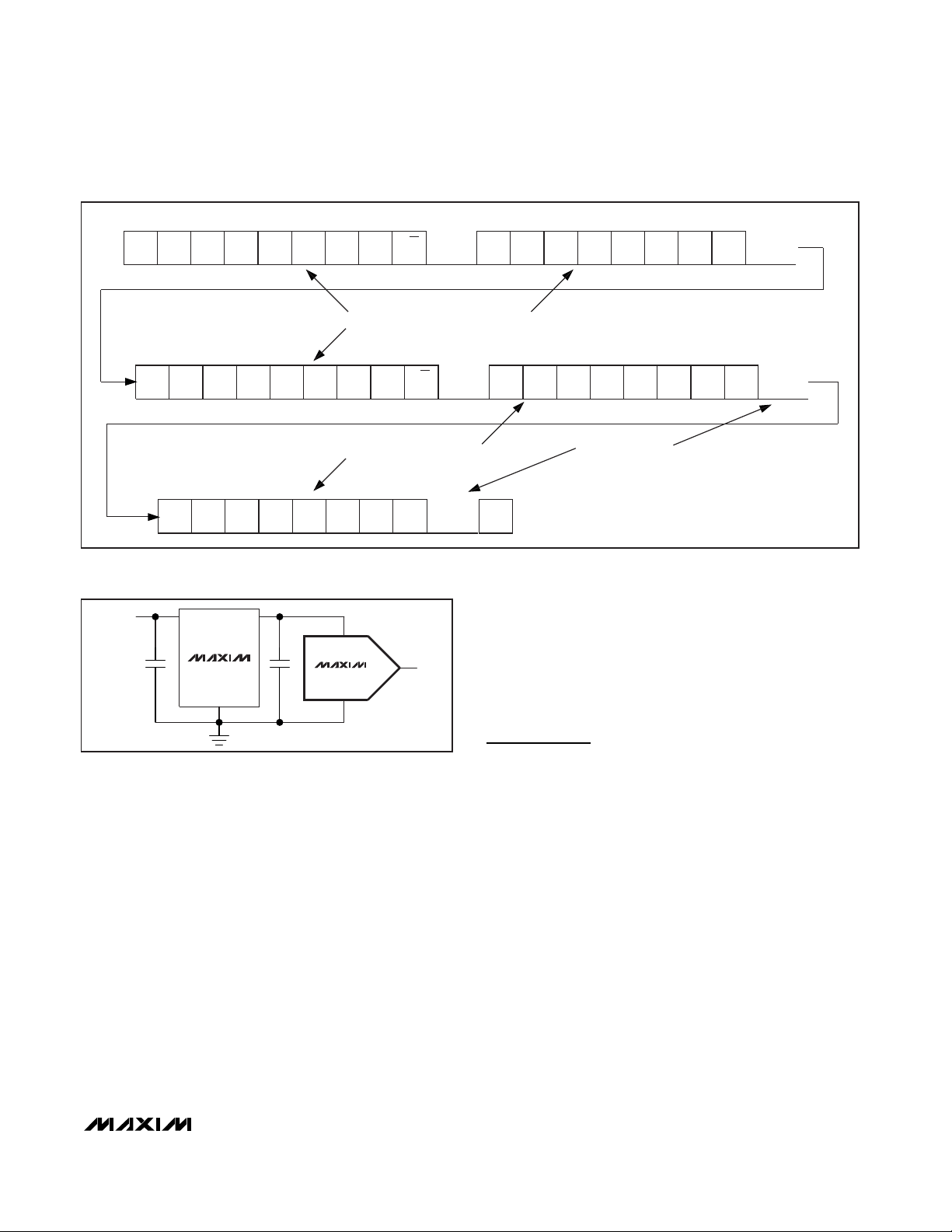
Applications Information
Powering the Device from an
External Reference
The MAX5811 uses the VDDas the DAC voltage reference. Any power-supply noise is directly coupled to the
device output. The circuit in Figure 8 uses a precision
voltage reference to power the MAX5811, isolating the
device from any power-supply noise. Powering the
MAX5811 in such a manner greatly improves overall
performance, especially in noisy systems. The
MAX6030 (3V, 75ppm/°C) or the MAX6050 (5V,
75ppm/°C) precision voltage references are ideal
choices due to the low power requirements of the
MAX5811.
Digital Inputs and Interface Logic
The MAX5811 2-wire digital interface is I2C and SMBus
compatible. The two digital inputs (SCL and SDA) load
the digital input serially into the DAC. Schmitt-trigger
buffered inputs allow slow-transition interfaces such as
SA6
A5
A4 A3 A2 A1 A0 C3 C2
X
XX XXX
Sr A6
A5
A4 A3 A2 A1 A0
MSB LSB MSB LSB
LSBMSB
ACK
ACK
ACK
D5 D4 D3 D2 D1 D0 X X
MSB LSB
ACK
ACK P
R/W
= 1
XX
PD1
PD0 D9 D8 D7 D6
MSB LSB
DATA BYTES GENERATED BY MASTER DEVICE
DATA BYTES GENERATED BY MAX5811
ACK GENERATED BY
MASTER DEVICE
R/W
= 0
Figure 7. Read Word Data Sequence
V
DD
IN
GND
GND
OUT
OUT
MAX5811
MAX6030/
MAX6050
Figure 8. Powering the MAX5811 from an External Reference
Page 12

MAX5811
optocouplers to interface directly to the device. The
digital inputs are compatible with CMOS logic levels.
Power-Supply Bypassing and
Ground Management
Careful PC board layout is important for optimal system
performance. Keep analog and digital signals separate
to reduce noise injection and digital feedthrough. Use a
ground plane to ensure that the ground return from
GND to the power-supply ground is short and low
impedance. Bypass VDDwith a 0.1µF capacitor to
ground as close to the device as possible.
Chip Information
TRANSISTOR COUNT: 7172
PROCESS: BiCMOS
10-Bit Low Power 2-Wire Interface Serial,
Voltage-Output DAC
12 ______________________________________________________________________________________
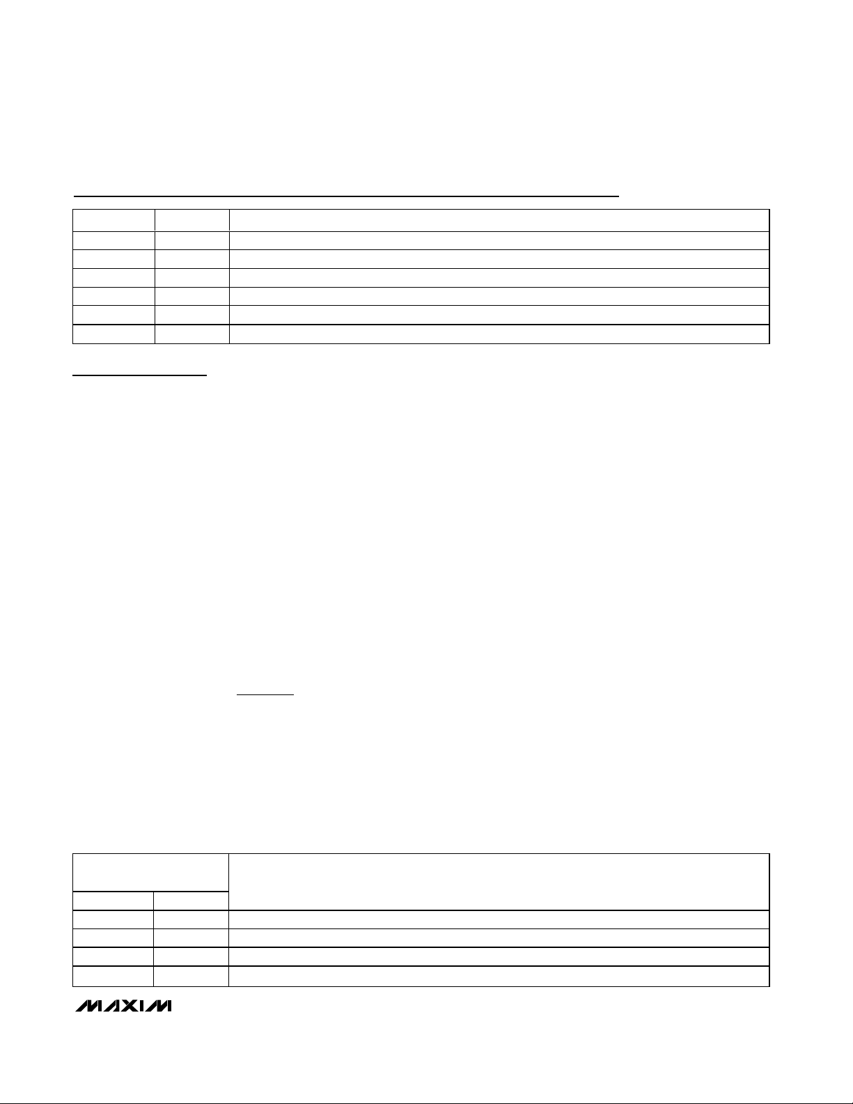
10-BIT
DAC
INPUT
REGISTER
MUX AND DAC
REGISTER
RESISTOR
NETWORK
POWER-DOWN
CIRCUITRY
SERIAL
INTERFACE
V
DD
SDA ADD SCL GND
OUT
MAX5811
Functional Diagram
Selector Guide
PART ADDRESS
MAX5811LEUT 0010 00X
MAX5811MEUT 0010 01X
MAX5811NEUT 0110 10X
MAX5811PEUT 1010 10X
Page 13

MAX5811
10-Bit Low Power 2-Wire Interface Serial,
Voltage-Output DAC
Maxim cannot assume responsibility for use of any circuitry other than circuitry entirely embodied in a Maxim product. No circuit patent licenses are
implied. Maxim reserves the right to change the circuitry and specifications without notice at any time.
Maxim Integrated Products, 120 San Gabriel Drive, Sunnyvale, CA 94086 408-737-7600 ____________________ 13
© 2004 Maxim Integrated Products Printed USA is a registered trademark of Maxim Integrated Products.
6LSOT.EPS
Package Information
(The package drawing(s) in this data sheet may not reflect the most current specifications. For the latest package outline information
go to www.maxim-ic.com/packages
.)
 Loading...