

Page 1
General Description
The MAX5722 dual,12-bit, low-power, buffered voltageoutput, digital-to-analog converter (DAC) is packaged
in a space-saving 8-pin µMAX package (5mm ✕ 3mm).
The wide supply voltage range of +2.7V to +5.5V and
112µA supply current accommodates low-power and
low-voltage applications. DAC outputs employ on-chip
precision output amplifiers that swing Rail-to-Rail®. The
MAX5722’s reference input accepts a voltage range
from 0 to VDD. In power-down, the reference input is
high impedance, further reducing the system’s total
power consumption.
The 20MHz, 3-wire SPI™, QSPI™, MICROWIRE™, and
DSP-compatible serial interface save board space and
reduce the complexity of opto- and transformer-isolated
applications. The MAX5722 on-chip power-on reset
(POR) circuit resets the DAC outputs to zero and loads
the output with a 100kΩ resistor to ground. This provides additional safety for applications that drive valves
or other transducers that need to be off on power-up.
The MAX5722’s software-controlled power-down
reduces supply current to less than 0.3µA and provides
software-selectable output loads (1kΩ, 100kΩ, or high
impedance) while in power-down. The MAX5722 is
specified over the -40°C to +125°C automotive temperature range.
Applications
Automatic Tuning
Gain and Offset Adjustment
Power Amplifier Control
Process Control I/O Boards
Battery-Powered Instruments
VCO Control
Features
♦ Ultra-Low Power Consumption
112µA at V
DD
= +3.6V
135µA at VDD= +5.5V
♦ Wide +2.7V to +5.5V Single-Supply Range
♦ 8-Pin µMAX Package
♦ 0.3µA Power-Down Current
♦ Guaranteed 12-Bit Monotonicity (±1LSB DNL)
♦ Safe Power-Up Reset to Zero Volts at DAC Output
♦ Three Software-Selectable Power-Down
Impedances (100kΩ, 1kΩ, Hi-Z)
♦ Fast 20MHz, 3-Wire SPI, QSPI, and MICROWIRE-
Compatible Serial Interface
♦ Rail-to-Rail Output Buffer Amplifiers
♦ Schmitt-Triggered Logic Inputs for Direct
Interfacing to Optocouplers
♦ Wide -40°C to +125°C Operating Temperature
Range
MAX5722
12-Bit, Low-Power, Dual, Voltage-Output
DAC with Serial Interface
________________________________________________________________ Maxim Integrated Products 1
Pin Configuration
19-2124; Rev 2; 7/03
For pricing, delivery, and ordering information, please contact Maxim/Dallas Direct! at
1-888-629-4642, or visit Maxim’s website at www.maxim-ic.com.
Rail-to-Rail is a registered trademark of Nippon Motorola, Inc.
SPI and QSPI are trademarks of Motorola, Inc.
MICROWIRE is a trademark of National Semiconductor, Corp.
Ordering Information
Functional Diagram appears at end of data sheet.
查询MAX5722供应商
PART TEMP RANGE PIN-PACKAGE
MAX5722EUA -40°C to +85°C 8 µMAX
MAX5722AUA -40°C to +125°C 8 µMAX
TOP VIEW
1
V
DD
2
MAX5722
3
CS
4
µMAX
87OUTB
OUTAGND
REF
6
DINSCLK
5
Page 2
MAX5722
12-Bit, Low-Power, Dual, Voltage-Output
DAC with Serial Interface
2 _______________________________________________________________________________________
ABSOLUTE MAXIMUM RATINGS
ELECTRICAL CHARACTERISTICS
(VDD= +2.7V to +5.5V, GND = 0, V
REF
= VDD, RL= 5kΩ, CL= 200pF, TA= T
MIN
to T
MAX
, unless otherwise noted. Typical values are
V
DD
= +5V, TA= +25°C.)
Stresses beyond those listed under “Absolute Maximum Ratings” may cause permanent damage to the device. These are stress ratings only, and functional
operation of the device at these or any other conditions beyond those indicated in the operational sections of the specifications is not implied. Exposure to
absolute maximum rating conditions for extended periods may affect device reliability.
VDDto GND..............................................................-0.3V to +6V
OUT_, SCLK, DIN, CS, REF to GND.............-0.3 to (V
DD
+ 0.3V)
Maximum Continuous Current Into Any Pin......................±50mA
Continuous Power Dissipation (T
A
= +70°C)
8-Pin µMAX (derate 4.6 mW/°C above +70°C) ............362mW
Operating Temperature Range .........................-40°C to +125°C
Junction Temperature......................................................+150°C
Storage Temperature Range .............................-65°C to +150°C
Lead Temperature (soldering, 10s) .................................+300°C
STATIC ACCURACY (Note 1)
Resolution N 12 Bits
Integral Nonlinearity Error INL (Note 2) ±2 ±16 LSB
Differential Nonlinearity Error DNL Guaranteed monotonic (Note 2) ±1 LSB
Zero-Code Error OE Code = 000 0.4 1.5 % of FS
Zero-Code Tempco 2.3 ppm/°C
Gain Error GE Code = FFF hex ±3 % of FS
Gain-Error Tempco 0.26 ppm/°C
Power-Supply Rejection Ratio PSRR Code = FFF hex, ∆VDD = ±10% 58.8 dB
REFERENCE INPUT
Reference Input Voltage Range V
Reference Input Impedance R
Power-Down Reference Current In power-down mode (Note 3) 1 10 µA
DAC OUTPUT
Output Voltage Range No load (Note 4) 0 V
DC Output Impedance Code = 800 hex 0.8 Ω
Short-Circuit Current
Wake-Up Time
Output Leakage Current
PARAMETER SYMBOL CONDITIONS MIN TYP MAX UNITS
REF
REF
In operation 64 90 126 kΩ
In power-down mode 2 MΩ
VDD = +3V 15
= +5V 48
V
DD
VDD = +3V 8
= +5V 8
V
DD
Power-down mode = output high
impedance
0V
±18 nA
DD
DD
V
V
mA
µs
Page 3
MAX5722
12-Bit, Low-Power, Dual, Voltage-Output
DAC with Serial Interface
_______________________________________________________________________________________ 3
ELECTRICAL CHARACTERISTICS (continued)
(VDD= +2.7V to +5.5V, GND = 0, V
REF
= VDD, RL= 5kΩ, CL= 200pF, TA= T
MIN
to T
MAX
, unless otherwise noted. Typical values are
V
DD
= +5V, TA= +25°C.)
TIMING CHARACTERISTICS
(VDD= 2.7V to 5.5V, GND = 0, TA= T
MIN
to T
MAX
, unless otherwise noted.)
Note 1: DC specifications are tested without output loads.
Note 2: Linearity is guaranteed from code 115 to code 3981.
Note 3: Limited with test conditions.
Note 4: Offset and gain error limit the FSR.
Note 5: Guaranteed by design.
PARAMETER SYMBOL CONDITIONS MIN TYP MAX UNITS
DIGITAL INPUTS (SCLK, DIN, CS)
Input High Voltage V
Input Low Voltage V
Input Leakage Current I
Input Capacitance C
DYNAMIC PERFORMANCE
Voltage-Output Slew Rate SR 0.5 V/µs
Voltage-Output Settling Time 400 hex to C00 hex (Note 5) 4 10 µs
Digital Feedthrough Any digital inputs from 0 to V
Digital Analog Glitch Impulse
DAC-to-DAC Crosstalk 2.4 nV-s
POWER REQUIREMENTS
Supply Voltage Range V
Supply Current with No Load I
Power-Down Supply Current I
VDD = +3V, +5V
IH
VDD = +3V, +5V
IL
IN
Digital inputs = 0 or V
IN
Major carry transition (code 7FF hex to code
800 hex)
DD
DD
DDPD
All digital inputs at 0 or V
All digital inputs at 0 or V
All digital inputs at 0 or V
0.7 x
V
DD
DD
±0.1 ±1µA
5pF
DD
0.15 nV-s
12 nV-s
2.7 5.5 V
= 3.6V 112 205
DD
= 5.5V 135 215
DD
= 5.5V 0.29 1 µA
DD
0.3 x
V
DD
V
V
µA
PARAMETER SYMBOL CONDITIONS MIN TYP MAX UNITS
SCLK Clock Frequency f
SCLK Pulse Width High t
SCLK Pulse Width Low t
CS Fall to SCLK Rise Setup Time t
SCLK Fall to CS Rise Setup Time t
DIN to SCLK Fall Setup Time t
DIN to SCLK Fall Hold Time t
CS Pulse Width High t
SCLK
CH
CL
CSS
CSH
DS
DH
CSW
020MHz
25 ns
25 ns
10 ns
10 ns
15 ns
0ns
80 ns
Page 4
MAX5722
12-Bit, Low-Power, Dual, Voltage-Output
DAC with Serial Interface
4 _______________________________________________________________________________________
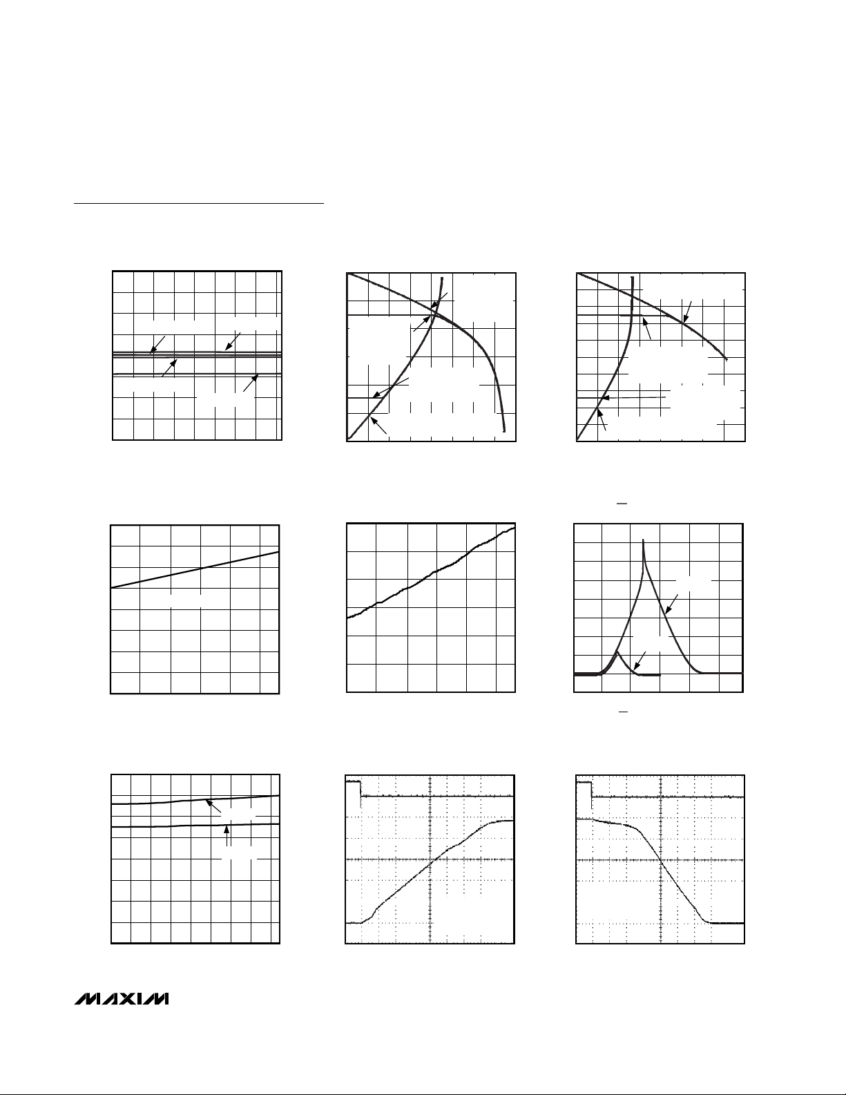
Typical Operating Characteristics
(V
REF
= VDD, TA= +25°C, unless otherwise noted.)
INTEGRAL NONLINEARITY vs.
CODE, T
16
12
8
4
0
INL (LSB)
-4
-8
-12
-16
0 512 1024 1536 2048 2560 3072 3584 4096
= +25°C
A
CODE
MAX5722 toc01
VDD = +5V
VDD = +3V
DIFFERENTIAL NONLINEARITY vs.
= +25°C
CODE, T
1.0
0.8
0.6
0.4
0.2
0
DNL (LSB)
-0.2
-0.4
-0.6
-0.8
-1.0
0 512 1024 1536 2048 2560 3072 3584 4096
A
CODE
1.0
0.8
MAX5722 toc02
0.6
0.4
0.2
0
-0.2
TOTAL UNADJUSTED ERROR (%)
-0.4
-0.6
0 512 1024 1536 2048 2560 3072 3584 4096
TOTAL UNADJUSTED ERROR vs.
CODE, T
VDD = +3V
= +25°C
A
VDD = +5V
CODE
MAX5722 toc03
INTEGRAL NONLINEARITY vs.
= -40°C
CODE, T
16
12
8
4
0
INL (LSB)
-4
-8
-12
-16
0 512 1024 1536 2048 2560 3072 3584 4096
A
VDD = +5V
VDD = +3V
CODE
INTEGRAL NONLINEARITY vs.
= +125°C
CODE, T
16
12
8
4
0
INL (LSB)
-4
-8
-12
-16
0 512 1024 1536 2048 2560 3072 3584 4096
A
VDD = +5V
VDD = +3V
CODE
MAX5722 toc04
MAX5722 toc07
DIFFERENTIAL NONLINEARITY vs.
= -40°C
CODE, T
1.0
0.8
0.6
0.4
0.2
0
DNL (LSB)
-0.2
-0.4
-0.6
-0.8
-1.0
0 512 1024 1536 2048 2560 3072 3584 4096
A
CODE
DIFFERENTIAL NONLINEARITY vs.
= +125°C
CODE, T
1.0
0.8
0.6
0.4
0.2
0
DNL (LSB)
-0.2
-0.4
-0.6
-0.8
-1.0
0 512 1024 1536 2048 2560 3072 3584 4096
A
CODE
1.0
0.8
MAX5722 toc05
0.6
0.4
0.2
0
-0.2
TOTAL UNADJUSTED ERROR (%)
-0.4
-0.6
0 512 1024 1536 2048 2560 3072 3584 4096
1.0
0.8
MAX5722 toc08
0.6
0.4
0.2
0
-0.2
TOTAL UNADJUSTED ERROR (%)
-0.4
-0.6
0 512 1024 1536 2048 2560 3072 3584 4096
TOTAL UNADJUSTED ERROR vs.
= -40°C
CODE, T
A
VDD = +3V
VDD = +5V
CODE
TOTAL UNADJUSTED ERROR vs.
= +125°C
CODE, T
A
VDD = +3V
VDD = +5V
CODE
MAX5722 toc06
MAX5722 toc09
Page 5
MAX5722
12-Bit, Low-Power, Dual, Voltage-Output
DAC with Serial Interface
_______________________________________________________________________________________ 5
Typical Operating Characteristics (continued)
(V
REF
= VDD, TA= +25°C, unless otherwise noted.)
0
40
20
100
80
60
140
120
160
-40 20 40-20 0 60 80 100 120
MAX5722 toc16
TEMPERATURE (°C)
SUPPLY CURRENT (µA)
SUPPLY CURRENT
vs. TEMPERATURE
VDD = +5V
VDD = +3V
FULL-SCALE SETTLING TIME
(V
DD
= +5V)
MAX5722 toc18
V
OUT_
1V/div
1µs/div
V
SCLK
5V/div
CODE FFF HEX TO 000
R
L
= 5kΩ
C
L
= 200pF
WORST CASE INL AND DNL
vs. TEMPERATURE
16
12
8
4
0
-4
INL AND DNL (LSB)
MINIMUM DNL
-8
-12
-16
-40 0 20-20
MAXIMUM DNL
TEMPERATURE (°C)
MAXIMUM INL
MINIMUM INL
60 80 100 120
40
SUPPLY CURRENT
vs. SUPPLY VOLTAGE
160
140
120
100
80
60
SUPPLY CURRENT (µA)
40
20
0
2.7 3.73.2 4.2 4.7 5.2
CODE = 3FF HEX
SUPPLY VOLTAGE (V)
SOURCE-AND-SINK CURRENT CAPABILITY
3.0
2.5
MAX5722 toc10
CODE = C00
2.0
HEX, SOURCING
CURRENT
(V)
FROM OUT_
1.5
OUT
V
1.0
0.5
0
042 6 8 10121416
POWER-DOWN SUPPLY CURRENT
300
250
MAX5722 toc13
200
150
100
50
POWER-DOWN SUPPLY CURRENT (nA)
0
2.7 3.73.2 4.2 4.7 5.2
= +3V)
(V
DD
CODE = FFF
HEX, SOURCING
CURRENT
FROM OUT_
CODE = 400 HEX,
SINKING CURRENT
INTO OUT_
CODE = 000 HEX,
SINKING CURRENT INTO OUT_
I
SOURCE/SINK
(mA)
vs. SUPPLY VOLTAGE
SUPPLY VOLTAGE (V)
MAX5722 toc11
MAX5722 toc14
SOURCE-AND-SINK CURRENT CAPABILITY
= +5V)
(V
5.0
4.5
4.0
3.5
3.0
(V)
2.5
OUT
V
2.0
1.5
1.0
0.5
0
0105 152025303540
DD
CODE = FFF HEX, SOURCING
CURRENT FROM OUT_
CODE = C00 HEX,
SOURCING CURRENT
FROM OUT_
CODE = 000 HEX,
SINKING CURRENT INTO OUT_
I
SOURCE/SINK
SUPPLY CURRENT vs.
CS INPUT VOLTAGE
900
800
700
600
500
400
300
SUPPLY CURRENT (µA)
200
100
0
021 345
VDD = +3V
CS INPUT VOLTAGE (V)
CODE = 400 HEX,
SINKING CURRENT
INTO OUT_
(mA)
VDD = +5V
MAX5722 toc12
MAX5722 toc15
FULL-SCALE SETTLING TIME
= +5V)
(V
DD
CODE 000 TO FFF HEX
R
C
1µs/div
= 5kΩ
L
= 200pF
L
MAX5722 toc17
V
SCLK
5V/div
V
OUT_
1V/div
Page 6

MAX5722
12-Bit, Low-Power, Dual, Voltage-Output
DAC with Serial Interface
6 _______________________________________________________________________________________
Typical Operating Characteristics (continued)
(V
REF
= VDD, TA= +25°C, unless otherwise noted.)
EXITING POWER-DOWN
(V
DD
= +5V)
MAX5722 toc21
V
OUT_
1V/div
5µs/div
V
SCLK
5V/div
CODE 800 HEX
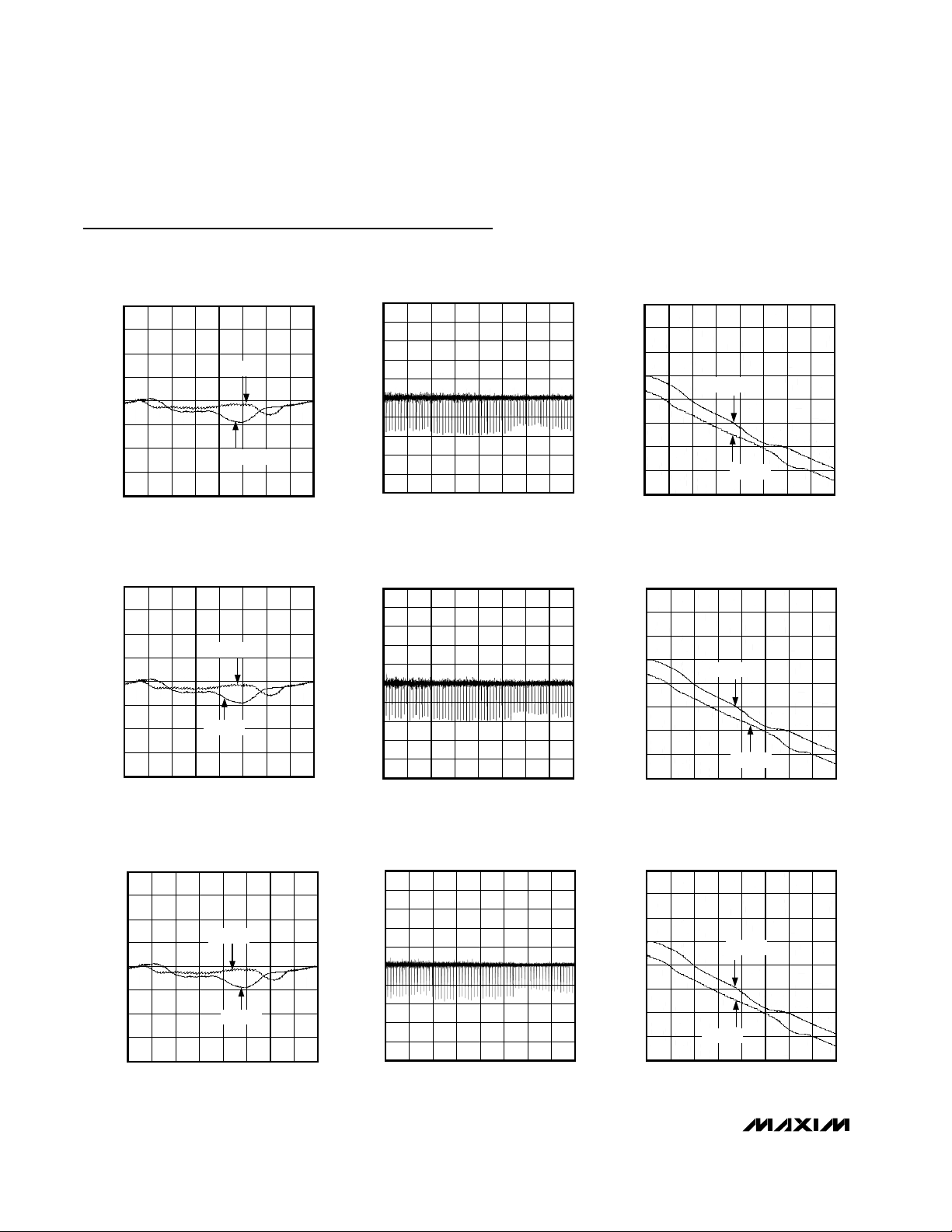
DIGITAL-TO-ANALOG GLITCH IMPULSE
(V
DD
= +5V)
MAX5722 toc22
V
OUT_
AC-COUPLED,
20mV/div
1µs/div
CODE 7FF HEX
TO 800 HEX
SCLK,
f
SCLK
= 500kHz
2V/div
DIGITAL-TO-ANALOG GLITCH IMPULSE
(V
DD
= +3V)
MAX5722 toc23
V
OUT_
AC-COUPLED,
50mV/div
1µs/div
CODE 7FF HEX
TO 800 HEX
SCLK,
f
SCLK
= 500kHz,
2V/div
DIGITAL-TO-ANALOG GLITCH IMPULSE
(V
DD
= +5V)
MAX5722 toc24
V
OUT_
AC-COUPLED,
50mV/div
1µs/div
CODE 800 HEX
TO 7FF HEX
SCLK,
f
SCLK
= 500kHz,
2V/div
HALF-SCALE SETTLING TIME
= +3V)
(V
DD
MAX5722 toc19
V
SCLK
5V/div
HALF-SCALE SETTLING TIME
= +3V)
(V
DD
MAX5722 toc20
V
SCLK
5V/div
CODE 400 HEX to
C00 HEX
R
C
1µs/div
= 5kΩ
L
= 200pF
L
V
OUT_
1V/div
CODE C00 HEX TO
400 HEX
R
L
C
L
1µs/div
= 5kΩ
= 200pF
V
OUT_
1V/div
Page 7

MAX5722
12-Bit, Low-Power, Dual, Voltage-Output
DAC with Serial Interface
_______________________________________________________________________________________ 7
Typical Operating Characteristics (continued)
(V
REF
= VDD, TA= +25°C, unless otherwise noted.)
POWER-ON RESET, SLOW RISE TIME
(V
DD
= +5V)
MAX5722 toc27
V
OUT_
AC-COUPLED,
2mV/div
40µs/div
VDD RISE
TIME = 76µs
V
DD
2V/div
POWER-ON RESET, FAST RISE TIME
(V
DD
= +3V)
MAX5722 toc28
V
OUT_
AC-COUPLED,
10mV/div
20µs/div
VDD RISE
TIME = 20µs
V
DD
2V/div
POWER-ON RESET, SLOW RISE TIME
(V
DD
= +3V)
MAX5722 toc29
V
OUT_
AC-COUPLED,
2mV/div
40µs/div
VDD RISE
TIME = 72µs
V
DD
2V/div
CLOCK FEEDTHROUGH
(V
DD
= +5V)
MAX5722 toc30
V
OUT_
AC-COUPLED,
1mV/div
100ns/div
SCLK
2V/div
f
SCLK
= 1MHz
DIGITAL-TO-ANALOG GLITCH IMPULSE
= +3V)
(V
DD
MAX5722 toc25
CODE 800 HEX
TO 7FF HEX
SCLK,
= 500kHz
f
SCLK
1V/div
V
OUT_
AC-COUPLED,
20mV/div
POWER-ON RESET, FAST RISE TIME
(V
DD
= +5V)
MAX5722 toc26
VDD RISE
TIME = 20µs
V
DD
2V/div
V
OUT_
AC-COUPLED,
10mV/div
1µs/div
20µs/div
Page 8

MAX5722
12-Bit, Low-Power, Dual, Voltage-Output
DAC with Serial Interface
8 _______________________________________________________________________________________
Typical Operating Characteristics (continued)
(V
REF
= VDD, TA= +25°C, unless otherwise noted.)
LINE TRANSIENT RESPONSE
(V
DD
= +3V)
MAX5722 toc33
V
OUT_
AC-COUPLED,
10mV/div
20µs/div
V
DD,
AC-COUPLED,
100mV/div
CROSSTALK
(V
DD
= +5V)
MAX5722 toc34
V
OUTB
AC-COUPLED,
1mV/div
4µs/div
CODE FFF HEX TO 00B HEX
V
OUTA
2V/div
CLOCK FEEDTHROUGH
= +3V)
(V
DD
f
= 1MHz
SCLK
MAX5722 toc31
SCLK
2V/div
LINE TRANSIENT RESPONSE
= +5V)
(V
DD
MAX5722 toc32
V
DD,
AC-COUPLED,
100mV/div
100ns/div
V
OUT_
AC-COUPLED,
1mV/div
20µs/div
V
OUT_
AC-COUPLED,
10mV/div
Page 9

MAX5722
12-Bit, Low-Power, Dual, Voltage-Output
DAC with Serial Interface
_______________________________________________________________________________________ 9
Detailed Description
The MAX5722 contains two 12-bit, voltage-output, lowpower, digital-to-analog converters (DACs). Each DAC
employs a resistor string architecture that converts a
12-bit digital input word to an equivalent analog output
voltage proportional to the applied reference voltage.
The MAX5722 shares one reference input (REF)
between both DACs. The MAX5722 includes rail-to-rail
output buffer amplifiers for each DAC, and input logic
for simple microprocessor (µP), and CMOS interfaces.
The power-supply range is from +2.7V to +5.5V
(Functional Diagram). The MAX5722’s reference input
accepts a voltage range from 0 to VDD. In power-down
mode the reference input is high impedance. The
MAX5722 is compatible with the 3-wire SPI, QSPI,
MICROWIRE, and DSP serial interface with Schmitt-triggered logic inputs.
Reference Input and DAC Output Range
The reference input accepts positive DC and AC signals. The voltage at REF sets the full-scale output voltage of both DACs. The reference input voltage range is
0 to VDD. The impedance at REF is 90kΩ. The voltage
at REF can vary from GND to VDD. The output voltages
(V
OUT_
) are represented by a digitally programmable
voltage source as:
V
OUT_
= (V
REF
✕
D) / 2
12
where D is the decimal equivalent of binary DAC input
code ranging from 0 to 4095. V
REF
is the voltage at
REF.
Output Buffer Amplifiers
All DACs are internally buffered at the output. The
buffer amplifiers have both rail-to-rail common mode
and (GND to V
REF
) output voltage range. The buffers
are unity-gain stable with CL = 200pF and RL = 5kΩ.
Buffer amplifiers are disabled during power-up and
individual DAC outputs are shorted to GND through a
100kΩ resistor. Buffer amplifiers can individually or altogether be powered-down by programming the input
register control bits. During power-down, contents of
the input and DAC registers remain the same. On
wake-up, all DAC outputs are restored to their prepower-down voltage values.
Power-Down Mode
In power-down mode, the DAC outputs are programmed to one of three output states, 1kΩ, 100kΩ, or
floating (Table 1). The REF input is high impedance
(2MΩ typ), to conserve current drain from the system
reference; therefore, the system reference does not
have to be powered-down. The DAC outputs return to
the values contained in the registers when brought out
of power-down. The recovery time, from total powerdown to power-up, is 8µs. This extra time is needed to
allow the internal bias to wake-up. Power-down mode
reduces current consumption to 0.3µA.
3-Wire Serial Interface
The MAX5722 digital interface is a standard 3-wire connection compatible with SPI/QSPI/MICROWIRE/DSP
interfaces. The chip-select input (CS) frames the serial
data loading at DIN. Immediately following CS high-to-
low transition, the data is shifted synchronously and
latched into the input register on the falling edge of the
serial clock input (SCLK). After 16 bits have been
loaded into the serial input register, it transfers its contents to the DAC latch. CS may then either be held low
or brought high. CS must be brought high for a minimum of 80ns before the next write sequence, since a
write sequence is initiated on a falling edge of CS. Not
Pin Description
PIN NAME FUNCTION
1VDDPower-Supply Input
2 GND Ground
3 CS Chip-Select Input
4 SCLK Serial-Clock Input
5 DIN Serial Data Input
6 REF External Reference Voltage Input
7, 8 OUTA, OUTB
DAC Voltage Outputs. Power-on reset sets DAC register to zero, and internally connects
OUT to GND with 100kΩ resistor.
Page 10

MAX5722
12-Bit, Low-Power, Dual, Voltage-Output
DAC with Serial Interface
10 ______________________________________________________________________________________
keeping CS low during the first 15 SCLK cycles discards input data. The serial clock (SCLK) can idle
either high or low between transitions.
The MAX5722 has two internal registers per DAC, the
input register and the DAC register. The input register
holds the data that is waiting to be shifted to the DAC
register. Both input registers can be loaded without
updating the output. This function is useful when both
outputs need to be updated at the same time. The input
register can be made transparent. When the input register is transparent, the data written into DIN loads
directly to the DAC register and the output is updated.
The DAC output is not updated until data is written to
the DAC register. See Table 2 for a list of serial-interface programming commands.
Power-On Reset (POR)
The MAX5722 has an internal POR circuit. At power-up,
all DACs are powered-down and OUT_ is terminated to
GND through 100kΩ resistors. Contents of input and
DAC registers are cleared to all zero. An 8µs recovery
time after issuing a wake-up command is needed
before writing to the DAC registers. Power-down mode
control commands can be applied immediately with no
recovery time.
C3-C0 are control bits. The data bits D11 to D0 are in
straight binary format. All zeros correspond to zero
scale and all ones correspond to full scale.
Digital Inputs
The digital inputs are compatible with CMOS logic. In
order to save power and reduce input to output coupling, SCLK and DIN input buffers are powered down
immediately after completion of shifting 16 bits into the
input shift register. A high to low transition at CS powers up SCLK and DIN input buffers.
Applications Information
Unipolar Output
The typical application circuit (Figure 3) shows the
MAX5722 configured for a unipolar output, where the
output voltages and the reference inputs have the
same polarity. Table 3 lists the unipolar output codes.
Bipolar Output
The MAX5722 can be configured for bipolar operation
using a dual supply op amp (Figure 4). The transfer
function for bipolar operation is:
where D is the decimal value of the DACs binary input
code. Table 4 shows digital codes (offset binary) and
corresponding output voltages for the circuit in Figure 4.
Table 1. Power-Down Mode Control
X = Don’t Care
EXTENDED
CONTROL
C3 C2 C1 C0 D11–D5 D4 D3 D2 D1 D0
1 1 1 1 X 0 X 0 0 0 DAC A DAC O/P, wake-up
1 1 1 1 X 0 X 0 0 1 DAC A Floating output
1 1 1 1 X 0 X 0 1 0 DAC A Output is terminated with 1kΩ
1 1 1 1 X 0 X 0 1 1 DAC A Output is terminated with 100kΩ
1 1 1 1 X 0 X 1 0 0 DAC B DAC O/P, wake-up
1 1 1 1 X 0 X 1 0 1 DAC B Floating output
1 1 1 1 X 0 X 1 1 0 DAC B Output is terminated with 1kΩ
1 1 1 1 X 0 X 1 1 1 DAC B Output is terminated with 100kΩ
1 1 1 1 X 1 X 0 0 0 DAC A-B DAC O/P, wake-up
1 1 1 1 X 1 X 0 0 1 DAC A-B Floating output
1 1 1 1 X 1 X 0 1 0 DAC A-B Output is terminated with 1kΩ
1 1 1 1 X 1 X 0 1 1 DAC A-B Output is terminated with 100kΩ
DATA BITS
DESCRIPTION FUNCTION
VV
=
OUT REF
D
2
4096
−
1
Page 11

MAX5722
12-Bit, Low-Power, Dual, Voltage-Output
DAC with Serial Interface
______________________________________________________________________________________ 11
Figure 1. 16-Bit Input Word
Figure 2. Timing Diagram
Figure 3. Typical Operating Circuit, Unipolar Output
Figure 4. Bipolar Output Circuit
CONTENTS OF SHIFT REGISTER
B15 (MSB) B0 (LSB)
C3 C2 C1 C0 D11 D10 D9 D8 D7 D6 D5 D4 D3 D2 D1 D0
t
t
CL
CH
SCLK X 1 2 3
t
t
OS
OH
X C3 C2 C1 C0 D11 D10 D0D1 XDIN
t
CSW
CS
t
CSS
456 16X
t
CSH
+2.7V TO +5.5V
IN
MAX6050
GND
REF
OUT
DAC_
GND
V
DD
MAX5722
OUT_
R1
+2.7V TO +5.5V
V
REF
DAC_
DD
MAX5722
OUT_
R1 = R2
R2
V+
V
OUT
-V
Page 12

MAX5722
12-Bit, Low-Power, Dual, Voltage-Output
DAC with Serial Interface
12 ______________________________________________________________________________________
+
V
REF
4095
4096
+
V
REF
2049
4096
+
V
REF
2047
4096
+
V
REF
2
+
V
REF
2047
2048
+
V
REF
1
2048
−V
REF
2047
2048
−V
REF
1
2048
+
V
REF
1
4096
−V
REF
Table 3. Unipolar Code Table Table 4. Bipolar Code Table
X = Don’t Care
Table 2. Serial-Interface Programming Commands
CONTROL DATA BITS
C3 C2 C1 C0 D11–D0
0000 X A
0001 X B
0 1 0 0 X A Data shifted to input register, OUTA unchanged
0 1 0 1 X B Data shifted to input register, OUTB unchanged
1 0 0 0 X A Shift data from input register to DAC register, OUTA updated
1 0 0 1 X B Shift data from input register to DAC register, OUTB updated
1 1 0 0 X A-B
1 1 0 1 X A-B Data shifted to input registers, OUTA and OUTB unchanged
1 1 1 0 X A-B Shift data from input registers to DAC registers, OUTA and OUTB updated
DAC CONTENTS ANALOG OUTPUT
1111 1111 1111
DAC FUNCTION
Input register transparent, data shifted directly to DAC register, OUTA
updated
Input register transparent, data shifted directly to DAC register, OUTB
updated
Input registers transparent, data shifted directly to DAC registers, OUTA
and OUTB updated
DAC CONTENTS ANALOG OUTPUT
1111 1111 1111
1000 0000 0001
1000 0000 0000
0111 1111 1111
0000 0000 0001
0000 0000 0000 0
1000 0000 0001
1000 0000 0000 0
0111 1111 1111
0000 0000 0001
0000 0000 0000
Page 13

MAX5722
12-Bit, Low-Power, Dual, Voltage-Output
DAC with Serial Interface
______________________________________________________________________________________ 13
Power Supply and Layout Considerations
Careful PC board layout is important for optimal system
performance. To reduce noise injection and digital feedthrough and keep analog and digital signals separate.
Ensure that that the return path from GND to the supply
ground is short and low impedance. Use a ground
plane. Bypass VDDto GND with a 0.1µF capacitor as
close as possible to VDD.
Chip Information
TRANSISTOR COUNT: 7737
PROCESS: BiCMOS
Functional Diagram
V
DD
INPUT
REGISTER A
INPUT
REGISTER B
INPUT CONTROL
LOGIC AND SHIFT
REGISTER
DAC
REGISTER B
DAC
REGISTER B
REF
POWER-DOWN
CONTROL LOGIC
12-BIT DAC A
12-BIT DAC B
OUTPUT
BUFFER
OUTPUT
BUFFER
MAX5722
OUTA
RESISTOR
NETWORK
OUTB
RESISTOR
NETWORK
CS
SCLK
DIN
GND
Page 14

MAX5722
12-Bit, Low-Power, Dual, Voltage-Output
DAC with Serial Interface
Maxim cannot assume responsibility for use of any circuitry other than circuitry entirely embodied in a Maxim product. No circuit patent licenses are
implied. Maxim reserves the right to change the circuitry and specifications without notice at any time.
14 ____________________Maxim Integrated Products, 120 San Gabriel Drive, Sunnyvale, CA 94086 408-737-7600
© 2003 Maxim Integrated Products Printed USA is a registered trademark of Maxim Integrated Products.
Package Information
(The package drawing(s) in this data sheet may not reflect the most current specifications. For the latest package outline information,
go to www.maxim-ic.com/packages.)
8
0.6±0.1
0.6±0.1
1
TOP VIEW
A2
e
FRONT VIEW
ÿ 0.50±0.1
D
b
E H
A1
4X S
BOTTOM VIEW
A
c
L
SIDE VIEW
8
1
DIM
A
A1
A2
b
c
D
e
E
H
L
α
S
INCHES
MIN
-
0.002
0.030
0.010
0.005
0.116
0.0256 BSC
0.116
0.188
0.016
0∞
0.0207 BSC
0.043
0.006
0.037
0.014
0.007
0.120
0.120
0.198
0.026
MAX
6∞
MILLIMETERS
MIN
0.05 0.15
0.25 0.36
0.13 0.18
2.95 3.05
2.95 3.05
4.78
0.41
MAX
- 1.10
0.950.75
0.65 BSC
5.03
0.66
0.5250 BSC
8LUMAXD.EPS
6∞0∞
α
PROPRIETARY INFORMATION
TITLE:
PACKAGE OUTLINE, 8L uMAX/uSOP
REV.DOCUMENT CONTROL NO.APPROVAL
21-0036
1
J
1
 Loading...