19-0198; Rev 0; 10/93
+3.3V-Powered, EIA/TIA-562 Dual Transceiver
with Receivers Active in Shutdown
_______________General Description
The MAX563 is a +3.3V-powered EIA/TIA-562 transceiver
with two transmitters and two receivers. Because it implements the EIA/TIA-562 standard, the MAX563 communicates with RS-232 transceivers, yet consumes far less
power; this makes it ideal for battery-powered, hand-held
computers. And, the MAX563 guarantees a 116kbps data
rate while maintaining ±3.7V EIA/TIA-562 signal levels,
which makes it compatible with LapLink™ software.
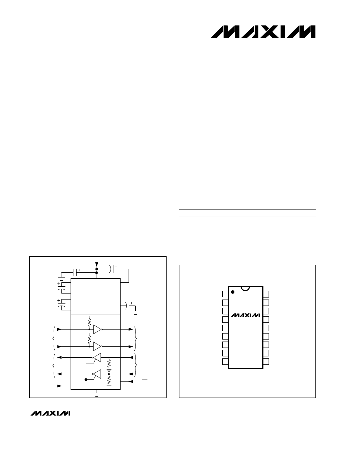
An on-board charge pump converts the +3.3V supply to
the ±6.6V needed to produce the EIA/TIA-562 output voltage levels. Four 0.1µF charge-pump capacitors and a
bypass capacitor of similar size are the only external components required.
When the MAX563’s charge pumps and transmitters are
shut down to save power, the receivers remain active to
continuously monitor signals from external devices (for
example, ring indicator from modems). The two receivers’
outputs can be enabled and disabled independently of the
shutdown function to allow two ports—generally of different
types—to be wire-OR connected at the UART.
________________________Applications
Handiterminals
Battery-Powered Equipment
Bar-Code Readers
Notebook and Palmtop Computers
____________________________Features
♦ Guaranteed Interoperability with RS-232
♦ Operates from a Single +3.0V to +3.6V Supply
♦ 2 Drivers, 2 Receivers
♦ Receivers Active in Shutdown Mode
♦ Low-Power Shutdown: 10µA Max
♦ Small Package—18-Pin Wide SO
♦ Three-State TTL/CMOS Receiver Outputs
♦ 116kbps Guaranteed Data Rate
______________Ordering Information
PART TEMP. RANGE PIN-PACKAGE
MAX563CPN 0°C to +70°C 18 Plastic DIP
MAX563CWN 0°C to +70°C 18 Wide SO
MAX563C/D 0°C to +70°C Dice *
* Dice are specified at T
= +25°C.
A
MAX563
__________Typical Operating Circuit
+3.3V
C3
ALL CAPACITORS 0.1µF
V+
OUT
OUT
+6.6V
3
-6.6V
7
V-
IN
IN
18
C4
15
RS-562
8
14
9
OUTPUTS
RS-562/RS-232
INPUTS
ON/OFF
17
V
CC
VOLTAGE DOUBLER
VOLTAGE INVERTER
V
CC
V
CC
5k
5k
GND
T1
T2
R1
R2
SHDN
CMOS
INPUTS
CMOS
OUTPUTS
2
C1+
C1
4
C1-
5
C2
C2+
6
C2-
400k
T1
12
IN
400k
11
T2
IN
R1
13
OUT
10
R2
OUT
1
EN
™ LapLink is a registered trademark of Traveling Software, Inc.
________________________________________________________________
__________________Pin Configuration
TOP VIEW
18
17
16
15
14
13
12
11
10
SHDN
V
CC
GND
T1
OUT
R1
IN
R1
OUT
T1
IN
T2
IN
R2
OUT
1
T2
R2
EN
C1+
V+
C1-
C2+
C2-
OUT
1
2
3
4
MAX563
5
6
7
V-
8
9
IN
DIP/SO
Maxim Integrated Products
Call toll free 1-800-998-8800 for free samples or literature.

+3.3V-Powered, EIA/TIA-562 Dual Transceiver
with Receivers Active in Shutdown
ABSOLUTE MAXIMUM RATINGS
Power Supply Ranges
Supply Voltage (V
Input Voltages
.........................................................-0.3V to (VCC-0.3V)
T
IN
...............................................................................±25V
R
IN
(Note 1)...................................................................±15V
T
OUT
Output Voltages
MAX563
Note 1: Input voltage measured with T
Stresses beyond those listed under “Absolute Maximum Ratings” may cause permanent damage to the device. These are stress ratings only, and functional
operation of the device at these or any other conditions beyond those indicated in the operational sections of the specifications is not implied. Exposure to
absolute maximum rating conditions for extended periods may affect device reliability.
.............................................................................±15V
T
OUT
....................................................-0.3V to (VCC+0.3V)
R
OUT
Driver/Receiver Output Short Circuit to GND.........Continuous
)...........................................-0.3V to +6V
CC
in high-impedance state. SHDN or VCC= 0V.
OUT
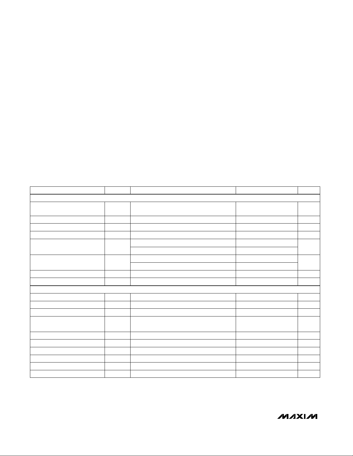
ELECTRICAL CHARACTERISTICS
(VCC= 3.0V to 3.6V, C1-C4 = 0.1µF, TA= T
PARAMETER
RS-562 TRANSMITTERS
Output Voltage Swing
Data Rate 200 116 kbpsRL= 3kΩ, CL= 1000pF, TA= +25°C
Input Logic Threshold Low
Input Logic Threshold High V
Logic Pull-Up/Input Current
Output Leakage Current
Transmitter Output Resistance 300 10M Ω
Output Short-Circuit Current V
RS-232/RS-562 RECEIVERS
Input Voltage Operating Range
Input Threshold Low V
Input Threshold High
Input Hysteresis 0.1 0.5 1.0 V
Input Resistance
Output Voltage Low V
Output Voltage High V
Output Leakage Current
EN Input Threshold Low
EN Input Threshold High
SYMBOL MIN TYP MAX
V
V
R
OL
OH
V
V
to T
MIN
IL
IH
IL
IH
IN
IL
IH
, unless otherwise noted.)
MAX
All transmitter outputs loaded with 3kΩ to
GND
SHDN = V
SHDN = 0V
VCC= 3.6V, SHDN = 0V, V
V
CC
VCC= V+ = V- = 0V, V
OUT
VCC= 3.3V
VCC= 3.3V
SHDN = VCC= 3.3V (no hysteresis when
SHDN = 0V)
I
OUT
I
OUT
EN = VCC, 0V ≤ V
CC
= SHDN = 0V, V
= 0V
= 3.2mA
= -0.5mA
Continuous Power Dissipation (T
Plastic DIP....................................................................889mW
Wide SO.......................................................................762mW
Operating Temperature Range...............................0°C to +70°C
Storage Temperature Range.............................-65°C to +160°C
Lead Temperature (soldering, 10sec).............................+300°C
CONDITIONS
= ±15V
OUT
= ±15V
OUT
= ±2V
OUT
≤ V
OUT
CC
= +70°C)
A
±3.7 ±4.5 V
0.6 V
2.4 V
220
±0.01 ±1
±0.01 ±10
±0.01 ±10
±15 ±60 mA
±25
0.4
2.4 V
357kΩ
0.2 0.4 V
VCC-0.6 VCC-0.2 V
±0.05 ±10 µA
0.6 V
2.4 V
UNITS
µA
µA
V
V
2 _______________________________________________________________________________________

+3.3V-Powered, EIA/TIA-562 Dual Transceiver
with Receivers Active in Shutdown
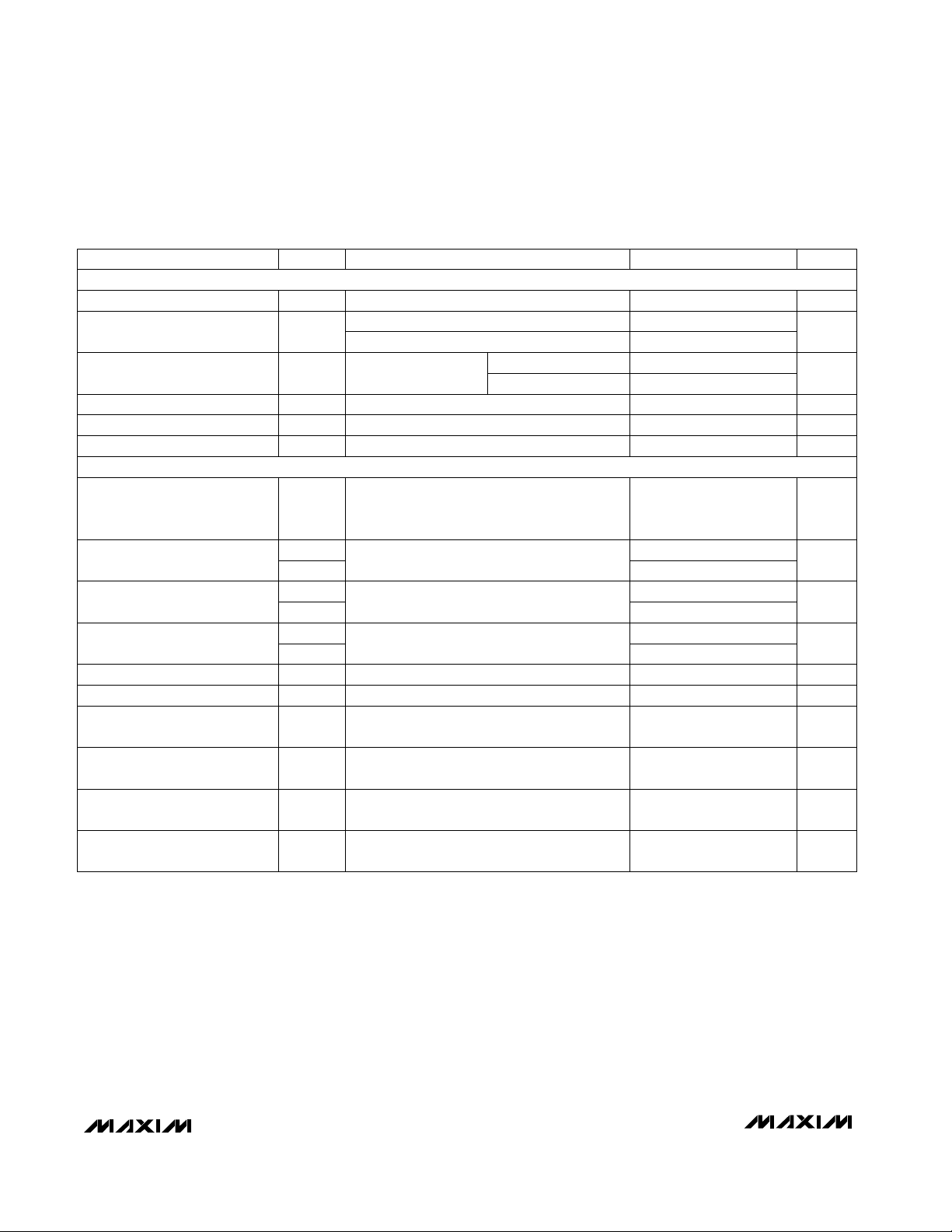
ELECTRICAL CHARACTERISTICS (continued)
(VCC= 3.0V to 3.6V, C1-C4 = 0.1µF, TA= T
PARAMETER
POWER SUPPLY
Operating Supply Voltage V
VCCSupply Current I
Shutdown Supply Current I
SHDN Input Leakage Current
SHDN Threshold Low
SHDN Threshold High
AC CHARACTERISTICS
Transition Slew Rate 4630V/µs
Transmitter Propagation Delay
Receiver Propagation Delay
(Normal Operation)
Receiver Propagation Delay
(Shutdown)
Receiver-Output Enable Time t
Receiver-Output Disable Time t
Transmitter-Output Enable
Time
Transmitter-Output Disable
Time
Transmitter Propagation Delay
Skew
Receiver Propagation Delay
Skew (Normal Operation)
SYMBOL MIN TYP MAX UNITS
CC
CC
CC
V
IL
V
IH
t
PHLT
t
PLHT
t
PHLR
t
PLHR
t
PHLS
t
PLHS
ER
DR
t
ET
t
DT
t
PHLT –
t
PLHT
t
PHLR –
t
PLHR
to T
MIN
No load
RL= 3kΩ on both outputs, inputs static
Figure 1
CL= 50pF to 2500pF, RL= 3kΩ to 7kΩ,
VCC= 3.3V, TA= +25°C, measured from
+3V to -3V or -3V to +3V (Note 2)
Figure 2
Figure 3
Figure 3
Figure 4
Figure 4
Includes charge pump start-up
Figure 5
, unless otherwise noted.)
MAX
CONDITIONS
TA= +25°C
TA= T
MIN
to T
MAX
3.0 3.6 V
38
8
0.1 10
250
0.1 ±1 µA
0.6 V
2.4 V
1.3 3.5
1.5 3.5
0.5 1.0
0.6 1.0
0.5 10.0
2.5 10.0
125 500 ns
160 500 ns
300 µs
600 ns
300 ns
100 ns
MAX563
mA
µA
µs
µs
µs
Note 2: Minimum slew rate is specified with CL= 1000pF for data rates above 20kbps, corresponding with EIA/TIA-562.
__________________________________________________________________________
 Loading...