

19-0198; Rev 0; 10/93
+3.3V-Powered, EIA/TIA-562 Dual Transceiver
with Receivers Active in Shutdown
_______________General Description
The MAX563 is a +3.3V-powered EIA/TIA-562 transceiver
with two transmitters and two receivers. Because it implements the EIA/TIA-562 standard, the MAX563 communicates with RS-232 transceivers, yet consumes far less
power; this makes it ideal for battery-powered, hand-held
computers. And, the MAX563 guarantees a 116kbps data
rate while maintaining ±3.7V EIA/TIA-562 signal levels,
which makes it compatible with LapLink™ software.
An on-board charge pump converts the +3.3V supply to
the ±6.6V needed to produce the EIA/TIA-562 output voltage levels. Four 0.1µF charge-pump capacitors and a
bypass capacitor of similar size are the only external components required.
When the MAX563’s charge pumps and transmitters are
shut down to save power, the receivers remain active to
continuously monitor signals from external devices (for
example, ring indicator from modems). The two receivers’
outputs can be enabled and disabled independently of the
shutdown function to allow two ports—generally of different
types—to be wire-OR connected at the UART.
________________________Applications
Handiterminals
Battery-Powered Equipment
Bar-Code Readers
Notebook and Palmtop Computers
____________________________Features
♦ Guaranteed Interoperability with RS-232
♦ Operates from a Single +3.0V to +3.6V Supply
♦ 2 Drivers, 2 Receivers
♦ Receivers Active in Shutdown Mode
♦ Low-Power Shutdown: 10µA Max
♦ Small Package—18-Pin Wide SO
♦ Three-State TTL/CMOS Receiver Outputs
♦ 116kbps Guaranteed Data Rate
______________Ordering Information
PART TEMP. RANGE PIN-PACKAGE
MAX563CPN 0°C to +70°C 18 Plastic DIP
MAX563CWN 0°C to +70°C 18 Wide SO
MAX563C/D 0°C to +70°C Dice *
* Dice are specified at T
= +25°C.
A
MAX563
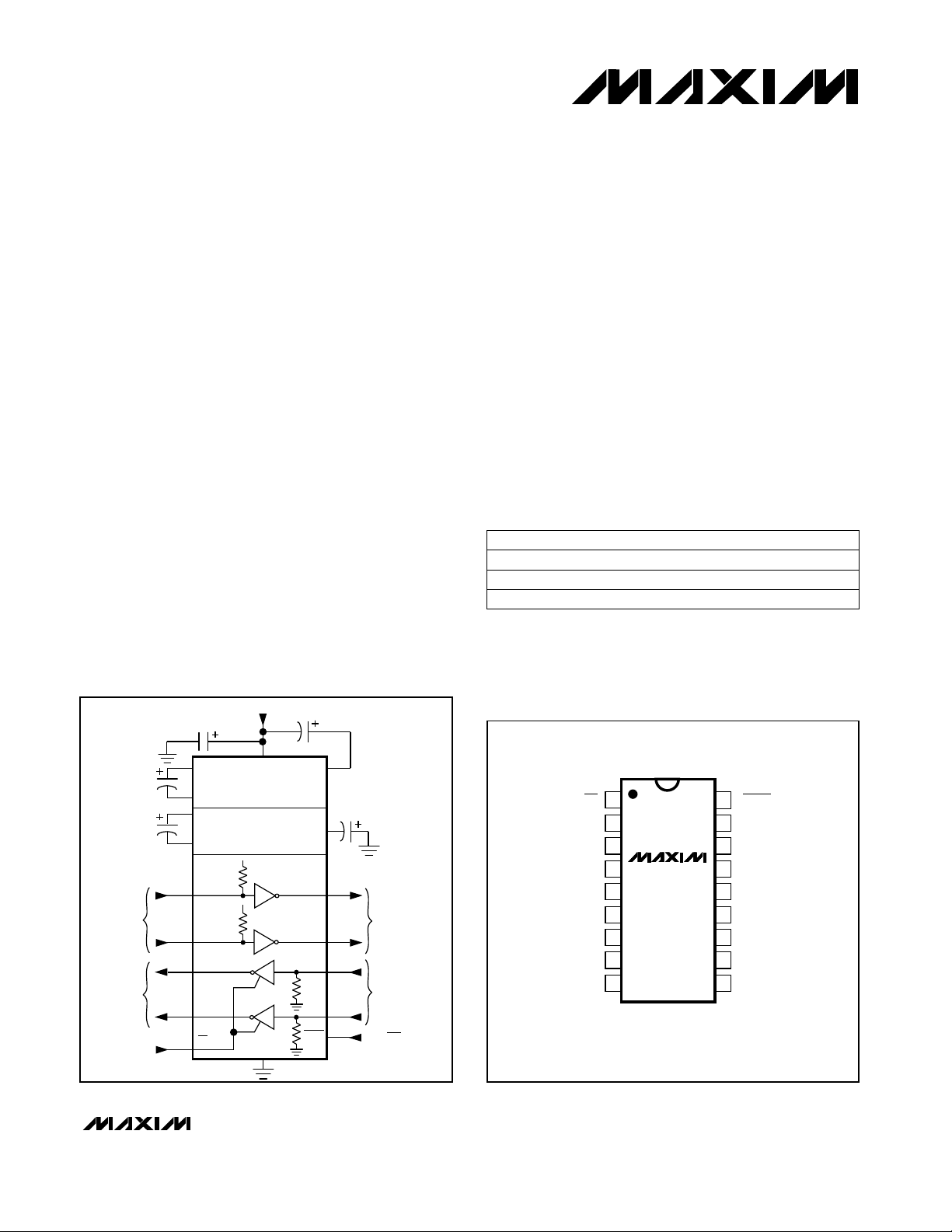
__________Typical Operating Circuit
+3.3V
C3
ALL CAPACITORS 0.1µF
V+
OUT
OUT
+6.6V
3
-6.6V
7
V-
IN
IN
18
C4
15
RS-562
8
14
9
OUTPUTS
RS-562/RS-232
INPUTS
ON/OFF
17
V
CC
VOLTAGE DOUBLER
VOLTAGE INVERTER
V
CC
V
CC
5k
5k
GND
T1
T2
R1
R2
SHDN
CMOS
INPUTS
CMOS
OUTPUTS
2
C1+
C1
4
C1-
5
C2
C2+
6
C2-
400k
T1
12
IN
400k
11
T2
IN
R1
13
OUT
10
R2
OUT
1
EN
™ LapLink is a registered trademark of Traveling Software, Inc.
________________________________________________________________
__________________Pin Configuration
TOP VIEW
18
17
16
15
14
13
12
11
10
SHDN
V
CC
GND
T1
OUT
R1
IN
R1
OUT
T1
IN
T2
IN
R2
OUT
1
T2
R2
EN
C1+
V+
C1-
C2+
C2-
OUT
1
2
3
4
MAX563
5
6
7
V-
8
9
IN
DIP/SO
Maxim Integrated Products
Call toll free 1-800-998-8800 for free samples or literature.
+3.3V-Powered, EIA/TIA-562 Dual Transceiver
with Receivers Active in Shutdown
ABSOLUTE MAXIMUM RATINGS
Power Supply Ranges
Supply Voltage (V
Input Voltages
.........................................................-0.3V to (VCC-0.3V)
T
IN
...............................................................................±25V
R
IN
(Note 1)...................................................................±15V
T
OUT
Output Voltages
MAX563
Note 1: Input voltage measured with T
Stresses beyond those listed under “Absolute Maximum Ratings” may cause permanent damage to the device. These are stress ratings only, and functional
operation of the device at these or any other conditions beyond those indicated in the operational sections of the specifications is not implied. Exposure to
absolute maximum rating conditions for extended periods may affect device reliability.
.............................................................................±15V
T
OUT
....................................................-0.3V to (VCC+0.3V)
R
OUT
Driver/Receiver Output Short Circuit to GND.........Continuous
)...........................................-0.3V to +6V
CC
in high-impedance state. SHDN or VCC= 0V.
OUT
ELECTRICAL CHARACTERISTICS
(VCC= 3.0V to 3.6V, C1-C4 = 0.1µF, TA= T
PARAMETER
RS-562 TRANSMITTERS
Output Voltage Swing
Data Rate 200 116 kbpsRL= 3kΩ, CL= 1000pF, TA= +25°C
Input Logic Threshold Low
Input Logic Threshold High V
Logic Pull-Up/Input Current
Output Leakage Current
Transmitter Output Resistance 300 10M Ω
Output Short-Circuit Current V
RS-232/RS-562 RECEIVERS
Input Voltage Operating Range
Input Threshold Low V
Input Threshold High
Input Hysteresis 0.1 0.5 1.0 V
Input Resistance
Output Voltage Low V
Output Voltage High V
Output Leakage Current
EN Input Threshold Low
EN Input Threshold High
SYMBOL MIN TYP MAX
V
V
R
OL
OH
V
V
to T
MIN
IL
IH
IL
IH
IN
IL
IH
, unless otherwise noted.)
MAX
All transmitter outputs loaded with 3kΩ to
GND
SHDN = V
SHDN = 0V
VCC= 3.6V, SHDN = 0V, V
V
CC
VCC= V+ = V- = 0V, V
OUT
VCC= 3.3V
VCC= 3.3V
SHDN = VCC= 3.3V (no hysteresis when
SHDN = 0V)
I
OUT
I
OUT
EN = VCC, 0V ≤ V
CC
= SHDN = 0V, V
= 0V
= 3.2mA
= -0.5mA
Continuous Power Dissipation (T
Plastic DIP....................................................................889mW
Wide SO.......................................................................762mW
Operating Temperature Range...............................0°C to +70°C
Storage Temperature Range.............................-65°C to +160°C
Lead Temperature (soldering, 10sec).............................+300°C
CONDITIONS
= ±15V
OUT
= ±15V
OUT
= ±2V
OUT
≤ V
OUT
CC
= +70°C)
A
±3.7 ±4.5 V
0.6 V
2.4 V
220
±0.01 ±1
±0.01 ±10
±0.01 ±10
±15 ±60 mA
±25
0.4
2.4 V
357kΩ
0.2 0.4 V
VCC-0.6 VCC-0.2 V
±0.05 ±10 µA
0.6 V
2.4 V
UNITS
µA
µA
V
V
2 _______________________________________________________________________________________
+3.3V-Powered, EIA/TIA-562 Dual Transceiver
with Receivers Active in Shutdown
ELECTRICAL CHARACTERISTICS (continued)
(VCC= 3.0V to 3.6V, C1-C4 = 0.1µF, TA= T
PARAMETER
POWER SUPPLY
Operating Supply Voltage V
VCCSupply Current I
Shutdown Supply Current I
SHDN Input Leakage Current
SHDN Threshold Low
SHDN Threshold High
AC CHARACTERISTICS
Transition Slew Rate 4630V/µs
Transmitter Propagation Delay
Receiver Propagation Delay
(Normal Operation)
Receiver Propagation Delay
(Shutdown)
Receiver-Output Enable Time t
Receiver-Output Disable Time t
Transmitter-Output Enable
Time
Transmitter-Output Disable
Time
Transmitter Propagation Delay
Skew
Receiver Propagation Delay
Skew (Normal Operation)
SYMBOL MIN TYP MAX UNITS
CC
CC
CC
V
IL
V
IH
t
PHLT
t
PLHT
t
PHLR
t
PLHR
t
PHLS
t
PLHS
ER
DR
t
ET
t
DT
t
PHLT –
t
PLHT
t
PHLR –
t
PLHR
to T
MIN
No load
RL= 3kΩ on both outputs, inputs static
Figure 1
CL= 50pF to 2500pF, RL= 3kΩ to 7kΩ,
VCC= 3.3V, TA= +25°C, measured from
+3V to -3V or -3V to +3V (Note 2)
Figure 2
Figure 3
Figure 3
Figure 4
Figure 4
Includes charge pump start-up
Figure 5
, unless otherwise noted.)
MAX
CONDITIONS
TA= +25°C
TA= T
MIN
to T
MAX
3.0 3.6 V
38
8
0.1 10
250
0.1 ±1 µA
0.6 V
2.4 V
1.3 3.5
1.5 3.5
0.5 1.0
0.6 1.0
0.5 10.0
2.5 10.0
125 500 ns
160 500 ns
300 µs
600 ns
300 ns
100 ns
MAX563
mA
µA
µs
µs
µs
Note 2: Minimum slew rate is specified with CL= 1000pF for data rates above 20kbps, corresponding with EIA/TIA-562.
__________________________________________________________________________

+3.3V-Powered, EIA/TIA-562 Dual Transceiver
with Receivers Active in Shutdown
______________________________________________________________Pin Description
PIN
1
2
MAX563
3
4
5
6
7
8, 15
9, 14
10, 13
11, 12
16
17
18
NAME FUNCTION
EN Receiver enable. Connect EN to GND to enable receivers, and take EN high to disable receivers.
C1+ Positive terminal of positive charge-pump capacitor.
V+
C1- Negative terminal of positive charge-pump capacitor.
C2+ Positive terminal of inverting charge-pump capacitor.
C2- Negative terminal of inverting charge-pump capacitor.
V-
T2
, T1
OUT
OUT
R2IN, R1
R2
T2IN, T1
OUT
GND
V
SHDN
, R1
CC
IN
OUT
IN
+2VCCvoltage generated by the positive charge pump. The voltage on V+ collapses to
when SHDN is low.
V
CC
-2VCCvoltage generated by the inverting charge pump. The voltage on V- collapses to
GND when SHDN is low.
EIA/TIA-562 voltage-level transmitter outputs. These outputs are disabled (Hi-Z) when
SHDN is low.
EIA/TIA-562 and EIA/TIA-232 voltage-level receiver inputs.
CMOS receiver outputs. These outputs are active regardless of the state of SHDN. They
are enabled when EN is low, and disabled (Hi-Z) when EN is high.
CMOS driver inputs.
Ground.
+3.0V to +3.6V supply voltage.
Shutdown control. Connect to GND to shut down the charge pumps and the transmitters.
Take high to turn on the charge pumps and to enable the transmitters.
_______________Detailed Description
The MAX563 consists of three sections: charge-pump
voltage converters, transmitters (drivers), and
receivers. Both the transmitters and the receivers are
inverting.
+3V to ±6V, Dual Charge-Pump Voltage
Converter
Two charge pumps either invert or double the incoming
VCCto generate the voltages required by the transmitters. The first charge pump uses capacitor C1 to
double VCC; the resulting voltage is stored on the V+
reservoir capacitor. The second charge pump uses
capacitor C2 to invert V+; this negative voltage is
stored on the V- capacitor.
When SHDN is low, the charge pumps are turned off,
V+ is pulled down to VCCby a 1kΩ resistor, and Vrises to GND.
It is possible to draw some power from the V+ and Vpins for external use. However, doing so diminishes the
charge-pump output voltages and reduces noise margins, so it is not recommended.
The MAX563’s drivers are inverting level translators that
convert +3V logic inputs to EIA/TIA-562 voltage levels.
With a VCC supply of only 3.0V, the driver outputs
deliver the EIA/TIA-562 ±3.7V minimum specification
under worst-case conditions—when both transmitters
are loaded with 3kΩ receivers (either EIA/TIA-232 or
EIA/TIA-562).
The transmitters are fast: the guaranteed data rate with
standard loads is 116kbps, which is the highest rate
commonly used by PC-to-PC communication software,
such as LapLink. The highest practical data rate may
be reduced if the other communicating device (RS-562
or RS-232) is not as fast, or if the cables present an
excessive capacitive load (>1000pF). Each transmitter
is designed to drive a single receiver; transmitters can
be paralleled to drive multiple receivers.
When SHDN is low, the driver outputs are turned off.
Their output leakage currents are less than 10µA when
pulled to GND or when driven to ±15V. This enables
two transmitters to be connected to the same line, provided that one of them is always disabled by taking
EIA/TIA-562 Transmitters
SHDN low.
4 _______________________________________________________________________________________

+3.3V-Powered, EIA/TIA-562 Dual Transceiver
with Receivers Active in Shutdown
0.1µF
+3V
INPUT
OV
V+
V+
t
PHLT
OV
V-
0V
V-
0.1µF
T
OUT
R
IN
+3.6V
5k
3k
OUTPUT
t
PLHT
Figure 2. Transmitter Propagation Delay Timing
+3V
INPUT
50%
50%
+3.6V
0.1µF
0.1µF
0.1µF
0V +3.6V
DRIVE
+3.6V
I
SHDN
C1+
C1-
C2+
C2-
T
IN
R
OUT
EN
SHDN
V
CC
R1 & R2
V
CC
MAX563
400k
T1 & T2
GND
MAX563
Figure 1. Shutdown Current Test Circuit
The inputs of unused drivers may be left unconnected
because they have internal 400kΩ pull-ups to VCC.
Unused inputs may also be connected to GND or VCC,
but VCCprovides lower power consumption because of
the internal pull-ups.
EIA/TIA-562 and EIA/TIA-232 Receivers
The MAX563’s receivers convert ±3.7V to ±13.2V
EIA/TIA-562 signal levels into +3V logic levels; they are
rated to receive signals up to ±25V to accommodate
EIA/TIA-232 signals as well. Both receivers invert. Their
inputs are each equipped with an internal 5kΩ (nominal) terminating resistor connected to ground, and the
input logic thresholds are 0.4V and 2.4V. The positive
logic-low threshold (VIL) ensures the receiver outputs
remain high whenever their inputs are left open.
The receivers are active when EN is low, and have
high-impedance outputs when EN is high.
When SHDN is high, the receivers have hysteresis.
This produces clean output transitions, even with slowmoving input signals that exhibit moderate amounts of
noise and ringing. When shut down, the receivers have
no hysteresis, and the propagation delay increases.
Shutdown and Enable Control
The SHDN and EN controls are independent. Both
receivers are always active when EN is low. With EN
low and SHDN high, the receivers operate at full speed
V
OUTPUT
t
PHLR
t
PHLS
50%
50%
GND
t
PLHR
t
PLHS
CC
Figure 3. Receiver Propagation Delay Timing
and have hysteresis. When active in shutdown mode
(EN = SHDN = low), the receivers operate at reduced
power and speed, and without hysteresis.
The charge pumps and transmitters operate only when
SHDN is high; they are unaffected by EN. When shut
down (SHDN = low) or unpowered (VCC= 0V), the
transmitter outputs are high impedance if they are
backdriven with voltages not exceeding ±15V. The pullup resistors at the driver inputs are disconnected in
shutdown mode to save power. During shutdown, V+ is
pulled down to VCC, and V- rises to GND.
_______________________________________________________________________________________ 5

+3.3V-Powered, EIA/TIA-562 Dual Transceiver
with Receivers Active in Shutdown
EN
INPUT
MAX563
V
CC
RECEIVER
OUTPUT
= 150pF
C
L
EN
INPUT
RECEIVER
OUTPUTS
0V
t
ER
V
- 0.6V
CC
+0.4V
V
CC
0V
t
DR
VOH - 0.1V
0.5V
1kΩ
CC
R
VOL + 0.1V
L =
Figure 4. Receiver Output Enable and Disable Timing
__________Applications Information
Charge-Pump Capacitor Selection
Normally, 0.1µF capacitors can be used for all locations. To reduce output ripple, increase the values of
the V+ and V- capacitors. If your capacitors have a
very wide tolerance, consider using a nominal value a
little larger than 0.1µF to ensure that the actual capacitance does not fall below about 80nF. For circuits
designed to operate over a wide range of temperatures, consider using slightly larger capacitors to compensate for any loss of capacitance at temperature
extremes. No advantage is gained by using values
larger than 10µF.
+3V
SHDN
0V
t
V+
V-
A. TIMING DIAGRAM
1 OR 0
B. TEST CIRCUIT
T
X
DT
+3.7V
-3.7V
3k 50pF
Figure 5. Transmitter Output Disable Timing
0V
Power-Supply Decoupling
Use a capacitor with the same value as the chargepump capacitors.
6 _______________________________________________________________________________________

+3.3V-Powered, EIA/TIA-562 Dual Transceiver
with Receivers Active in Shutdown
Table 1. Summary of EIA/TIA-232E/V.28 and EIA/TIA-562 Specifications
CONDITIONPARAMETER
Driver Output Voltage
0 Level
1 Level
Maximum Output Level ±25V
Signal Rate (3kΩ≤RL≤7kΩ)
Receiver Input Thresholds
0 Level
1 Level
Maximum Input Level
Maximum Instantaneous Slew Rate
Maximum Driver Output Short-Circuit
Current
Transition Rate on Driver Output
Driver Output Resistance with Power Off -2V < V
3kΩ to 7kΩ load
No load
CL= 2500pF
CL= 1000pF
< 2V
OUT
EIA/TIA-232E/V.28
SPECIFICATION
5.0V to 15.0V
-5.0V to -15.0V
Up to 20kbps
Not defined
3.0V to 15.0V
-3.0V to -15.0V
±25V
30V/µs
100mA
V.28 1ms or 3% of the period
RS-232 4% of the period
300Ω
MAX563
EIA/TIA-562
SPECIFICATION
3.7V to 13.2V
-3.7V to -13.2V
±13.2V
Up to 20kbps
Up to 64kbps
3.0V to 15.0V
-3.0V to -15.0V
±25V
30V/µs
60mA
4V/µs
300Ω
Table 2. DB9/DB25 Cable Connections Commonly Used for EIA/TIA-232E, EIA/TIA-562 and V.24
Asynchronous Interfaces
DB25 PIN
1 DCD
2 RxD
3 TxD
4 DTR
5
6
7
9 Ring Indicator
8
3 Receiver Data
2 Transmit Data
20
7 Signal Ground
6
5
_______________________________________________________________________________________ 7
Received Line Signal Detector (sometimes called Data Carrier Detect)
Data Terminal Ready
Data Set Ready
Request to Send
Clear to Send8 CTS
NAMEDB9 PIN SYMBOL
GND
DSR
RTS4
RI22
FUNCTION
Handshake from DCE
Data from DCE
Data from DTE
Handshake from DTE
Reference point for signals
Handshake from DCE
Handshake from DTE
Handshake from DCE
Handshake from DCE

+3.3V-Powered, EIA/TIA-562 Dual Transceiver
with Receivers Active in Shutdown
___________________Chip Topography
V+
MAX563
C1-
C2+
C1+
EN
SHDN
GND
V
CC
T1
OUT
C2-
V-
T2
OUT
R2
OUT
T2
R2
IN
0.070"
(1.778 mm)
IN
TRANSISTOR COUNT: 189;
SUBSTRATE CONNECTED TO V+.
(2.667 mm)
R1
IN
R1
OUT
T1
IN
0.105"
Maxim cannot assume responsibility for use of any circuitry other than circuitry entirely embodied in a Maxim product. No circuit patent licenses are
implied. Maxim reserves the right to change the circuitry and specifications without notice at any time.
8
___________________Maxim Integrated Products, 120 San Gabriel Drive, Sunnyvale, CA 94086 (408) 737-7600
© 1993 Maxim Integrated Products Printed USA is a registered trademark of Maxim Integrated Products.
 Loading...